Threshold-Dependent Camouflaged Cells to Secure Circuits Against Reverse Engineering Attacks
Abstract
With current tools and technology, someone who has physical access to a chip can extract the detailed layout of the integrated circuit (IC). By using advanced visual imaging techniques, reverse engineering can reveal details that are meant to be kept secret, such as a secure protocol or novel implementation that offers a competitive advantage. A promising solution to defend against reverse engineering attacks is IC camouflaging. In this work, we propose a new camouflaging technique based on the threshold voltage of the transistors. We refer to these cells as threshold dependent camouflaged cells. Our work differs from current commercial solutions in that the latter use look-alike cells, with the assumption that it is difficult for the reverse engineer to identify the cell’s functionality. Yet, if a structural distinction between cells exists, then these are still vulnerable, especially as reverse engineers use more advanced and precise techniques. On the other hand, the proposed threshold dependent standard cells are structurally identical regardless of the cells’ functionality. Detailed circuit simulations of our proposed threshold dependent camouflaged cells demonstrate that they can be used to cost-effectively and robustly camouflage large netlists. Corner analysis of process, temperature, and supply voltage (PVT) variations show that our cells operate as expected over all PVT corners simulated.
I Introduction
The need to protect the intellectual property (IP) of integrated circuit (IC) design companies is increasing as threats from IC reverse engineering attacks become more prominent. Reverse engineering of ICs consists of using advanced depackaging, delayering and imaging techniques in order to acquire the gate-level netlist. Not only is it possible to successfully obtain the full layout and netlist of complex ICs fabricated using advanced processes [1], it is also commercially feasible, such that companies such as Chipworks [2] and Degate [3] offer these services. IC reverse engineering can cause the competitive advantage of a chip maker to diminish, as well as reveal details about the chip that are meant to be secret, for example, the implementation of a secure communication protocol [4].
IC camouflaging technology has been proposed [5, 6] as a way to counteract reverse engineering attacks. With this countermeasure, the designer aims to hinder the ability of the reverse engineer to visually decipher the functionality of a gate. For example, NAND and XOR gates are made visually similar by fabricating them with identical metal and polysilicon layers and contact locations. The difference lies in what type of contacts are placed. These contacts may either be true or dummy. The former electrically connects the two layers, and the latter has a small gap in the middle so that it behaves like an open circuit. The selection of which type of contact to use establishes the functionality of a gate.
The principal assumption in this method is that, due to imprecision in the etching process [5, 6], the attacker is unable to discriminate between true and dummy contacts. Consequently, the Boolean functionality of the camouflaged gate cannot be ascertained by exclusively using traditional reverse engineering techniques. This method is referred to as dummy contact based camouflaging.
The expectation that a reverse engineer’s capabilities and techniques will not improve and become more sophisticated and precise reveals a weakness in dummy contact based camouflaging. Indeed, ICs fabricated in advanced technology nodes down to 22 have been reverse engineered [1]. This illustrates that while visually discernible differences in layout structure exist, the threat from IC imaging based reverse engineering attacks will remain.
In this paper, we propose a new camouflaging technique that addresses this vulnerability. We present an approach that leverages the intrinsic characteristics of the material used instead of the physical structure of a camouflaged gate. For this reason the gate layout, including vias and contacts, is the same regardless of its Boolean functionality. Instead, the functionality of the proposed camouflaged gate is determined by the threshold voltage of its transistors, that is, depending on whether it has been fabricated using a high- or low- process. As such, this technique uses the standard features available in commercial CMOS dual-Vth (or multi-Vth) processes [7]. We call this technique threshold dependent (TD) camouflaging and the cells are called TD camouflaged cells. To the best of our knowledge, our work is the first to present a camouflaging solution that leverages commercial multi-Vth CMOS processes to camouflage the Boolean functionality of a gate depending on whether it has been fabricated using high- or low- transistors.
There are several advantages that result from using TD camouflaged cells. First, traditional etching and optical imaging techniques used by reverse engineers are ineffective since the functionality of the cell depends on the threshold voltage, which in turn is determined by the doping concentration of the cell. Second, even though an attacker can image and identify the doping concentration of a cell using methods such as spreading resistance profiling (SRP) and secondary ion mass spectrometry (SIMS), these have limited spatial resolution [8]. Other approaches involve using scanning capacitance probes. While these can offer higher spatial resolution they still have limited accuracy because they do not directly measure dopant concentration [8]. As Chipworks notes, physical features can potentially be reverse engineered deep into the nanometer scale “…with high-resolution electron microscopy, but obtaining details of the chemical composition of the structure is now in the realm of counting atoms” [9].
Our approach can be used in conjunction with a multi- process [7] in a cost effective manner. That is, each cell can be manufactured using either high- or low-, depending on the gate that it is replacing, which means that camouflaging cells results in up to different possible functions. Lastly, we note that TD camouflaged cells can be used in conjunction with dummy contact based camouflaged technique to make the reverse engineering problem even harder for an attacker.
II Contributions
The novel contributions of this work are:
-
•
Proposal of TD camouflaged cells, a logic cell whose Boolean functionality depends on its threshold voltage,
-
•
design, analysis and evaluation of a specific instance of a TD camouflaged cell that functions as either an AND or an OR gate depending on its threshold voltage, and
-
•
experimental results showing the robustness of TD camouflaged cells over process, voltage and temperature (PVT) corners, and comparing the delay and power overheads of TD camouflaged cells to conventional logic families.
The rest of this paper is organized as follows. In Section III, we describe previous work related to our paper. Section IV, presents and discusses the design of TD camouflaged cells as well as considerations for robustness to process variations. We report experimental results in Section V. Finally, we conclude our paper in Section VII.
III Related Work
The idea of controlling the functionality of a cell by using varying operating parameters has been previously proposed. For instance, [10, 11, 12, 13] explore the use of polymorphic gates. These cells are characterized by having different functionalities that change according to the variation of supply voltage or temperature. Since controlling temperature is complicated and determining the supply voltage of each gate is feasible, these cells cannot be used for IC camouflaging.
A previous notion that has been explored in the context of IC camouflaging is the use of look-alike cells [5, 6]. The functionality of these cells depend on the location of true and dummy contacts which are claimed to hinder the capability of the attacker to identify which vias are functional. Even though this technique is used to prevent the reverse engineering of an IC, it still relies on a physical structural difference, which may not deter a more skilled attacker.
Our proposed TD camouflaged cells are structurally identical, yet their function depends on an inherent characteristic of the transistor. Hence the attacker would require more sophisticated tools to “image” the threshold voltage of each cell since this is dependant on channel doping. Our cells can be used in addition to or instead of conventional dummy-contact based camouflaged cells.
There is some prior work involving threshold voltage based camouflaging [14, 15]. The first technique [14] uses selective ion implantation in certain transistors to ensure that these transistors become permanently “stuck-at” either logic 0 or logic 1 (essentially converting transistors to permanently on/off switches). This introduces two problems: (1) the required increase in channel doping is large, making it easier for an attacker to detect; and (2) the approach requires extra steps in the current CMOS flow. In contrast, TD camouflaged cells leverages existing, commercial multi-Vth processes, and requires much subtler changes in doping density. The latter [15] technique uses post-fabrication focused-ion beams (FIB) to alter doping concentration. This must be done individually for each chip, making it a slow and expensive process. Concurrently with our work, another approach for threshold-dependent camouflaging has been recently proposed. However, this approach requires the generation and distribution of additional precise voltages on the chip (besides VDD and ground), while having similar overheads as our technique [16]. Since the paper is currently an Arxiv draft made available only very recently, a thorough empirical comparison is left as future work.
Finally, note that recent work has also proposed stealthily changing the polarity of the diffusion layer for both attack [17] and defense [18]. In this, the polarity of the diffusion layer is changed. Attacks on these techniques that are able to reverse engineer the polarity of a diffusion layer (p- or n-type) [19] would not work for TD camouflaged cells since we only change the doping concentration, not polarity.
Given access to a camouflaging technique, prior work has also addressed the problem of which gates to camouflage so as to make it difficult for the attacker to reverse engineer their identities given the input/output behaviour of the chip [6]. A recent attack on this technique has demonstrated that the number of gates that needs to be camouflaged is much larger than previously thought [20]. Regardless, the question of which and how many gates in the netlist to camouflage is orthogonal to the work presented in this paper.
IV TD camouflaged cells
IV-A Basic Operating Principle
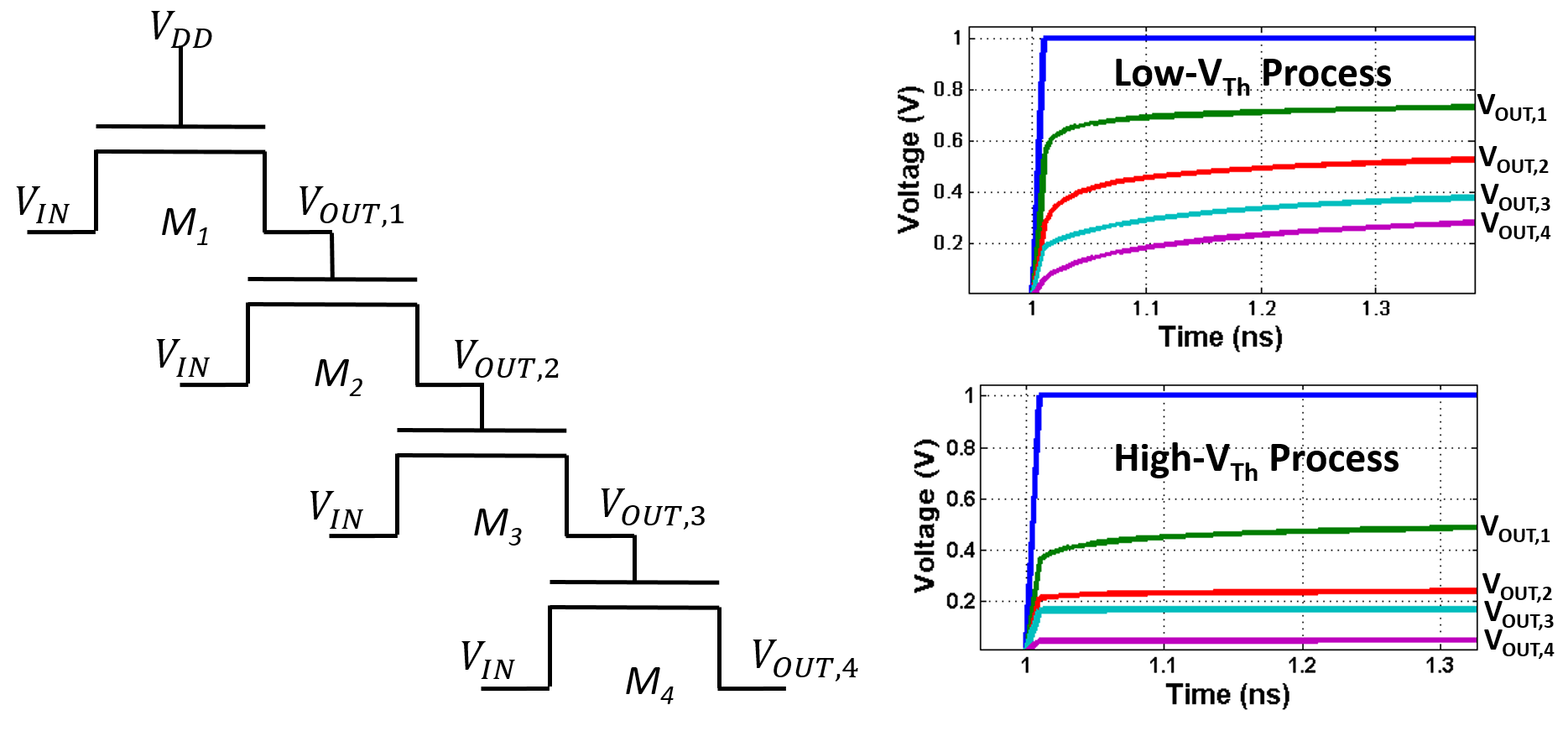
When transistor pass gates are connected in a cascade layout like in Figure 1 (Left),
the voltage at drops after each stage. In this layout, if is set to , then, the maximum voltage at will be . Consequently, if of is set to then, will be . As we continue to connect transistors in this way we can see that the voltage at the source can be characterized by , where is the number of stages of connected transistors. We make these assumptions for an ideal NMOS device with no sub-threshold leakage. Since depends on the doping concentration of the transistor, the voltage at the source of varies according to the threshold voltage asserted during the fabrication process.
Figure 1 (Left) shows the layout in which the NMOS transistors are connected as well as the output voltage at each source terminal for for each stage obtained from a simulation using Predictive Technology Models (PTM) [21] for a 22 technology for High- and for Low- processes. For each simulation all transistors in the layout were considered to have either High- or Low-. In Figure 1 (Right) we can see that the output voltage decreases at each stage, and more so for High- simulations than for Low-. Note that the difference between the theoretically expected and observed simulated results is due to the assumption of ideal transistors with
zero off-current, when, for 22 technology, sub-threshold conduction is non-negligible.
IV-B Threshold-Dependant Camouflaged Cells - AND/OR
IV-B1 Schematic Design
Using the previous principle we have developed a layout of a gate that can have the functionality of AND or OR depending on the threshold voltage that is asserted during the manufacturing process.
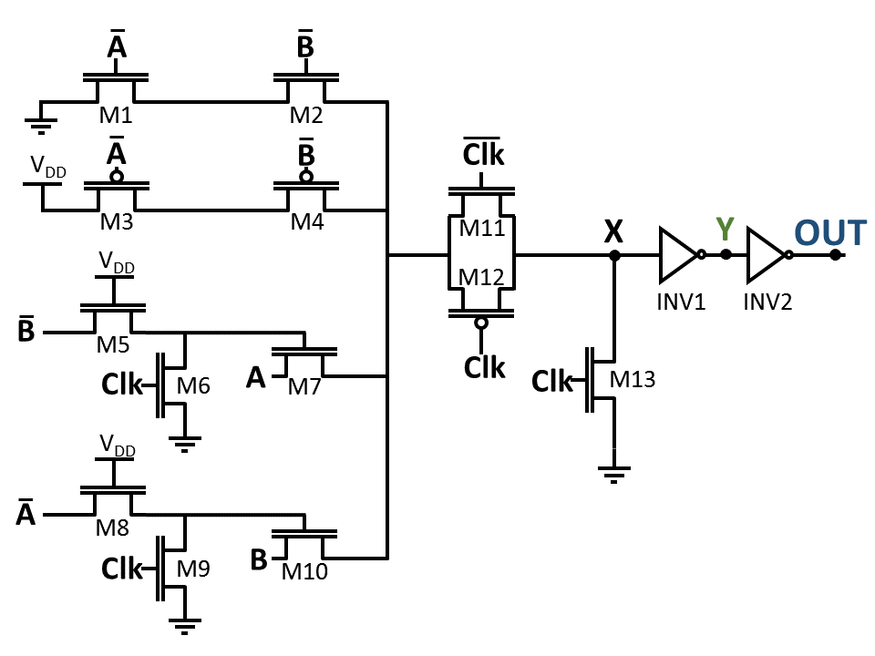
Figure 2 shows the schematic of our implementation of a camouflaged AND/OR gate. It is a clocked logic family (similar to domino logic). Our implementation has two phases of execution, a predischarge (PRE) and an evaluate (EVAL) phase. In the EVAL phase the clock CLK signal is logic 0, and it is 1 during the PRE phase.
The logic function is determined by the activation of one of the four cases (branches), each dealing with a unique possible input combination. The top two branches of the layout correspond to inputs and . We observe that the output is the same regardless of the function of the cell. For these cases transistors and are on while transistors and are off, or vice versa. The third branch corresponds to and . Here we notice that the output changes depending on whether the desired functionality is an OR or an AND cell. In order to be able to obtain different behaviour, we connect NMOS transistors and in the aforementioned cascaded layout. Since we have the same case for and , we connect NMOS transistors and in the same manner for last branch. In summary, we use the cascade configuration when we want to be able to pull down to zero a specific input combination depending on the manufacturing process.
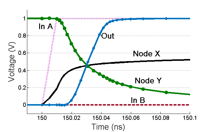
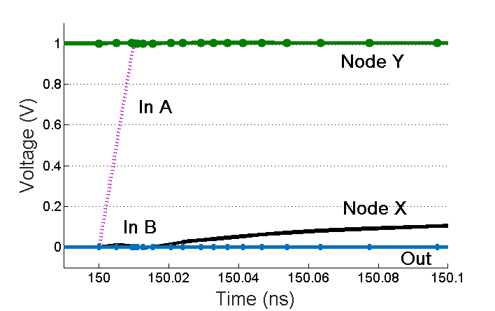
This different behaviour can be visualized in Figure 3. In the left, the voltage at Node X rises to , while in the right the voltage rises to . We determine that the first voltage is a logic 1 and the lower voltage is a logic 0 by setting the mid-point voltage of the succeeding inverter, INV1, between and . In this manner we can observe an accentuated difference at Node Y. In Figure 3 (Left), the voltage at Node Y falls below , while in Figure 3 (Right) the voltage remains close to . The final inverter, INV2, also skewed, provides clean logic levels at the output.
IV-B2 Clocked Logic
So far we have assumed, implicitly, that Node X is initialized to , and either stays at or transitions to . However, if Node X starts at then the output for the and case, as well as for the and , will stay at for the High- process. For correct operation as an AND gate, the output is expected to fall to . In order to deal with this complication we add NMOS transistors that pre-discharge the affected nodes. This technique is similar to the one used in dynamic logic cells. When , Node X is initialized to . We also need to pre-discharge the outputs of transistors and to eliminate accumulated charge at these nodes over multiple clock cycles. Our schematic is composed of the clocking transistors and . They are necessary to discharge the nodes periodically. Lastly, TD camouflaged cells operate as expected when the inputs transition from in the EVAL phase, which is like conventional dynamic logic. On the other hand, if the input transitions from during the EVAL phase, the output for the High- case may be incorrect. Consequently the proposed TD camouflaged cells are compatible with domino logic implementations, but cannot be used with static CMOS logic.
IV-C Integration With Domino Logic
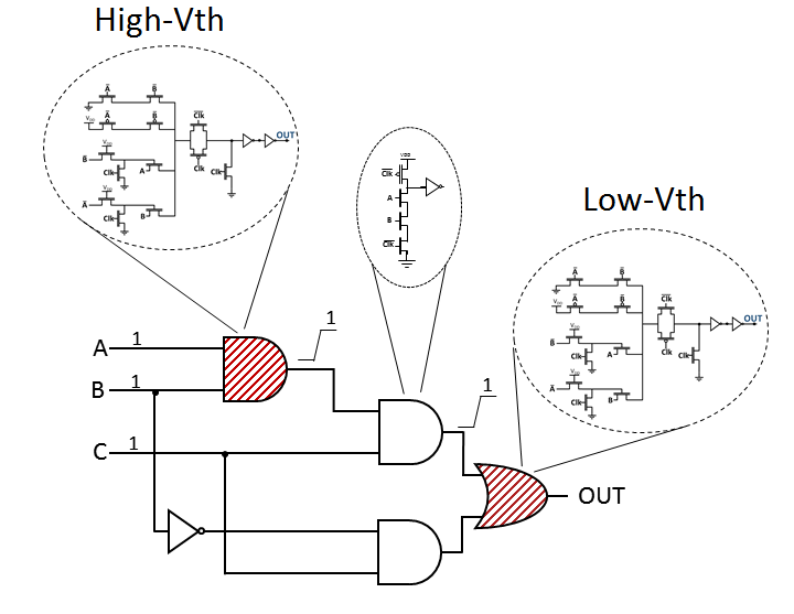
Domino logic [22] is a clocked logic design family in which each dynamic logic gate is followed by an inverting gate, for example, a static CMOS inverter. Domino logic has been used in commercial processor designs where speed is of the essence [23] and work on improving performance of dynamic logic [24] is ongoing. Domino logic gates implement non-complemented Boolean functions like AND and OR instead of complemented Boolean functions (such as NAND and NOR) like static CMOS. Therefore, once a transition occurs at the input, this will result in a transition at the output during the EVAL stage. A domino logic implementation netlist can be camouflaged using TD camouflaged cells by simply replacing conventional domino AND and domino OR gates with the proposed camouflaged AND/OR gate (Figure 4).
In Figure 4, the designer has chosen to camouflage two gates using TD camouflaged cells. By using reverse engineering techniques the attacker is unable to identify whether the TD camouflaged cells are ANDs or ORs, therefore the camouflaged netlist could implement one of four different Boolean logic functions: (i) ; (ii) ; (iii) ; and (iv) . The set of possible functions that a netlist with TD camouflaged cells could implement depends on the set of gates that are chosen. We note, however, that the question of how many and which gates to camouflage is out of the scope of our work and is not addressed here.
IV-D Universal Logic Family
Like Domino logic, TD camouflaged cells implement non-inverting logic gates. Therefore, a reasonable question to ask is — can any Boolean logic function be implemented using TD camouflaged cells? The answer is yes. This is done by ensuring that the primary inputs to the circuit are available in both true and complemented forms. Now, any Boolean logic function can be expressed in sum-of-product form using only true literals if the true and complemented form of every input is considered to be a separate variable. In other words, the function can be implemented using AND and OR gates if both true and complemented of the primary inputs are available.
Observe that although the complemented primary inputs can result in transition, these transitions can be guaranteed to occur during the precharge phase since they occur immediately after the clock edge. For instance, in the example netlist in Figure 4, observe that a transitions only occurs at the output of the static CMOS inverter driven by primary input . Provided that the propagation delay of the static CMOS inverter is less than the half period of the clock, these transitions will occur in the PRE phase and will not cause problems. All other transitions in the netlist only occur in the EVAL phase and are always transitions.
IV-E Robustness to Process Variation
Since our TD camouflaged cells depend on the threshold voltage, we must have careful consideration to the robustness to manufacturing process variations. Variations in doping concentration, which directly affect the operating threshold voltage, should not cause incorrect behaviour of the cell. In particular, even if the high- () and low- () implementations vary around their nominal values, TD camouflaged cells should continue to operate as AND and OR gates, respectively. We should specially consider the slow corner for and the fast corner for . Assuming that is the maximum difference (positive or negative) in threshold voltage, that () characterizes the slow corner for low-, and that () characterizes the fast corner for High-, for correct operation equation 1 is a condition that must be satisfied.
| (1) |
To satisfy 1, the mid-point voltage of INV1 must be set between and . We can achieve this by skewing INV1 so that the cut-off threshold voltage is suitable for detecting the logic 0 or 1 value that is reached by Node X in Fig. 2.
In Section V we establish a range of skew values for which the cell works correctly, including the aforementioned corner cases.
V Experimental Results
We have used 22 technology libraries from the ASU Process Technology Model (PTM) repository [21] for implementing our TD camouflaged cells. The 22 technology has customizable predictive model files for both high performance (low-) and low power (high-) transistors. We used the HSPICE circuit simulation tool for all simulations. The nominal supply voltage for this technology is . The variability in doping concentration is assumed to be of the nominal doping concentration for both the low power and high performance libraries.
First, we characterize the delay, power consumption and robustness of our proposed TD camouflaged cells. Then we present a case study by integrating TD camouflaged cells into a large benchmark netlist and analyze delay and power overheads as a function of the number of camouflaged gates.
V-A Robustness of TD camouflaged cells
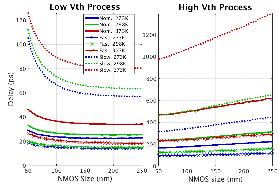
Our first goal is to size transistors so as to guarantee robustness against PVT variations. To do so, we considered process variations in threshold voltage 111This assumption is justified by results in [25] that indicate a of variation in threshold voltage to be 90 mV at 22 nm., temperature ranging from to and a range from to . Figure 5 shows the delay of the TD camouflaged cells on the y-axis versus size of the NMOS transistor in INV1 (for a fixed PMOS size) on the x-axis for different PVT corners. We find that the for NMOS sizes ranging between 50 and 250 , the cell works correctly over all PVT corners and for both the the low- and high- cases. We therefore picked an NMOS INV1 size of 80 .
V-B Power and Delay Characterization of TD camouflaged cells
In Table II we present the propagation delay and power consumption of the proposed TD camouflaged cells as well as conventional domino logic AND and OR gates. TD camouflaged cells with OR function (implemented with low- transistors) have a delay greater than a low- domino OR. Also, when a TD camouflaged cells functions as an AND gate (implementation with high- transistors), it presents a delay that is greater than a high- domino AND. From a power perspective, we note that the overheads for the TD camouflaged cells are and the corresponding values for the domino AND and OR gates, respectively.
| Static CMOS | Domino | TDCC | |||||||
| AND | OR | AND | OR | AND | OR | ||||
| Delay | Low | 7.68 | 11.26 | 9.93 | 4.98 | – | 25.7 | ||
| High | 34.03 | 50.47 | 66.00 | 23.63 | 269.8 | – | |||
| Power | |||||||||
| Low | 0.10 | 0.12 | 0.10 | 0.29 | - | 2.49 | |||
| 0.57 | 7.32 | 0.11 | 9.17 | - | 8.64 | ||||
| 0.13 | 5.92 | 0.37 | 9.17 | - | 8.07 | ||||
| 7.93 | 6.61 | 5.81 | 8.94 | - | 9.41 | ||||
| High | 0.00 | 0.00 | 0.02 | 0.01 | 0.13 | - | |||
| 0.96 | 1.55 | 0.01 | 3.36 | 0.37 | - | ||||
| 0.84 | 1.48 | 0.13 | 3.36 | 0.38 | - | ||||
| 1.29 | 1.49 | 1.66 | 3.78 | 1.65 | - | ||||
V-C Results of Netlist Integration of TD camouflaged cells
To provide a better understanding of the impact of the delay and power overheads caused by TD camouflaged cells we have integrated our camouflaged logic circuits into a benchmark netlist. The logic circuits are first implemented using domino logic after which a randomly chosen subset of gates is camouflaged. We have used random selection [26] in this work, yet other selection algorithms may also be used [6].
We have implemented an automated toolflow using the Berkeley SIS synthesis framework [27]. It’s input is combinational logic described in .pla format and outputs an implementation that can be implemented using domino logic (similar to Figure 4). To do this, we replace the complemented form of each variable with a new variable and input the new .pla file to SIS. The netlist that is used has non-complemented gates, and we further restrict our current implementation to the use of just AND and OR gates.
For our netlist integration of TD camouflaged cells we have used the benchmark apex5 from the MCNC benchmark suite. This benchmark has 234 inputs, 37 outputs, and 2382 product terms. The results are normalized to the uncamouflaged domino logic baseline implementation. For consistency, all AND gates were implemented using high- and all OR gates were implemented using low-, even though other selection criteria may be used. As expected, Table II presents results obtained from simulations. With 40% of the gates camouflaged the delay overhead is around 72.7% and power overhead is near 31%. These results may vary depending on which set of gates are chosen to be camouflaged and which non camouflaged gates will be fabricated with which process (high performance or low power). It is necessary to take into consideration the delay and power overheads as well as the critical path.
| Percent of Camouflaged Cells in Netlist | ||||
| 10% | 20% | 30% | 40% | |
| Delay | 1.3613 | 1.5153 | 1.6305 | 1.7270 |
| Power | 1.0770 | 1.1551 | 1.2327 | 1.3105 |
VI Possible Attacks
Like other camouflaging solutions, there are potential approaches that attackers could use to determine the identities of camouflaged gates. These include measuring the etch rate during chemical deprocessing, which could be used to determine which which transistor is more heavily doped. In addition, an attacker might use the difference in power and delay characteristics of camouflaged gates to determine their identities. However, all camouflaging techniques are susceptible to this attack to some degree. Finally, attackers might develop more accurate techniques to measure the doping concentration of transistor channels, but this represents that natural cat-and-mouse game between attackers and defenders.
VII Conclusion
This work proposes a new threshold dependent camouflaging technique that protects digital ICs against delayering and optical imaging based IC reverse engineering. Existing solutions consist of camouflaging Boolean functionality of a cell via the placement of true and dummy contacts, therefore they posses a vulnerability since they can be identified depending on the difference of the contacts. However, our proposed TD camouflaged cells only differ in operating threshold voltage and have the same physical structure regardless of their Boolean functionality. The threshold voltage of the cell depends on the inherent doping concentration of the transistor which cannot be determined by using traditional reverse engineering optical imaging techniques. Although other means for determining doping concentration exist, they have limited spatial resolution or accuracy.
We have presented an analysis of delay and power consumption overhead for our proposed TD camouflaged cells. This IC camouflaging alternative is based on a design that leverages the threshold-voltage dependent level shifting property cascaded pass gates, and is shown to be robust against process variations incurred during manufacturing. TD camouflaged cells can be seamlessly incorporated into a netlist with domino logic gates. Experimental results indicate that camouflaging up to of gates of the apex5 benchmark induced delay and power overheads near than and , respectively.
VIII Future Work
Consequently, our proposed TD camouflaged cells increase the effort necessary for attackers who wish to reverse engineer the netlist of a digital IC. Future work will focus on designing a more comprehensive library of TD camouflaged cells, further optimizing the delay, as well as power and robustness of TD camouflaged cells. Understanding vulnerabilities that may come from the analysis of side channels as well as defending against advanced attacks is crucial.
Acknowledgment
The authors acknowledge funding support from the NSF CNS Award #1527072, NSF CNS Award #1553419, and the Semiconductor Research Corporation.
References
- [1] Chipworks, “Intel’s 22-nm Tri-gate Transistors Exposed.” http://www.chipworks.com/en/technical-competitive-analysis/resources/blog/intels-22-nm-tri-gate-transistors-exposed/, Apr. 2012.
- [2] Chipworks, “Reverse Engineering Software.” http://www.chipworks.com/en/technical-competitive-analysis/resources/reerse-engineering-software. Last accessed May 2014.
- [3] Degate, “Reverse engineering integrated circuits with degate.” http://www.degate.org/documentation/. Last accessed May 2014.
- [4] Chipworks, “Inside the Apple Lightning Cable.” http://www.chipworks.com/en/technical-competitive-analysis/resources/blog/inside-the-apple-lightning-cable/, Oct. 2012.
- [5] SypherMedia, “Syphermedia library circuit camouflage technology.” http://www.smi.tv/solutions.htm. Last accessed May 2014.
- [6] J. Rajendran, M. Sam, O. Sinanoglu, and R. Karri, “Security Analysis of Integrated Circuit Camouflaging,” in Proceedings of the 2013 ACM SIGSAC Conference on Computer and Communications Security, CCS ’13, (New York, NY, USA), pp. 709–720, ACM, 2013.
- [7] J. Kao, A. Chandrakasan, and D. Antoniadis, “Transistor sizing issues and tool for multi-threshold cmos technology,” in Proceedings of the 34th annual Design Automation Conference, pp. 409–414, ACM, 1997.
- [8] Y. Huang, C. Williams, and H. Smith, “Direct comparison of cross-sectional scanning capacitance microscope dopant profile and vertical secondary ion-mass spectroscopy profile,” Journal of Vacuum Science & Technology B, vol. 14, no. 1, pp. 433–436, 1996.
- [9] R. Torrance and D. James, “Reverse engineering in the semiconductor industry,” in Custom Integrated Circuits Conference, 2007. CICC’07. IEEE, pp. 429–436, IEEE, 2007.
- [10] L. Sekanina, R. Ruzicka, Z. Vasicek, R. Prokop, and L. Fujcik, “Repomo32-new reconfigurable polymorphic integrated circuit for adaptive hardware,” in Evolvable and Adaptive Hardware, 2009. WEAH’09. IEEE Workshop on, pp. 39–46, IEEE, 2009.
- [11] A. Stoica, R. Zebulum, and D. Keymeulen, Polymorphic electronics. Springer, 2001.
- [12] R. Ruzicka, L. Sekanina, and R. Prokop, “Physical demonstration of polymorphic self-checking circuits,” in On-Line Testing Symposium, 2008. IOLTS’08. 14th IEEE International, pp. 31–36, IEEE, 2008.
- [13] A. Stoica, R. Zebulum, D. Keymeulen, and J. Lohn, “On polymorphic circuits and their design using evolutionary algorithms,” in In: Proc. of IASTED International Conference on Applied Informatics AI2002, Insbruck, Citeseer, 2002.
- [14] L. Larson, “Convertible multi-function microelectronic logic gate structure and method of fabricating the same,” Sept. 8 1992. US Patent 5,146,117.
- [15] R. Walden, “Dynamic circuit disguise for microelectronic integrated digital logic circuits,” Apr. 13 1993. US Patent 5,202,591.
- [16] A. Iyengar and S. Ghosh, “Threshold voltage-defined switches for programmable gates,” CoRR, vol. abs/1512.01581, 2015.
- [17] G. T. Becker, F. Regazzoni, C. Paar, and W. P. Burleson, “Stealthy dopant-level hardware trojans,” in Cryptographic Hardware and Embedded Systems-CHES 2013, pp. 197–214, Springer, 2013.
- [18] M. Shiozaki, R. Hori, and T. Fujino, “Diffusion programmable device: The device to prevent reverse engineering.,” IACR Cryptology ePrint Archive, vol. 2014, p. 109, 2014.
- [19] T. Sugawara, D. Suzuki, R. Fujii, S. Tawa, R. Hori, M. Shiozaki, and T. Fujino, “Reversing stealthy dopant-level circuits,” in Cryptographic Hardware and Embedded Systems–CHES 2014, pp. 112–126, Springer, 2014.
- [20] M. El-Massad, S. Garg, and M. Tripunitara, “Ic decamouflaging: Reverse engineering camouflaged ics within minutes,” in Network and Distributed System Security Symposium (NDSS), Internet Society, 2015.
- [21] W. Zhao and Y. Cao, “New generation of predictive technology model for sub-45 nm early design exploration,” Electron Devices, IEEE Transactions on, vol. 53, no. 11, pp. 2816–2823, 2006.
- [22] J. Rabaey, A. Chandrakasan, and B. Nikolic, Digital integrated circuits, A design perspective (Second Edition). Prentice Hall Publishers, 2003.
- [23] B. Stackhouse, S. Bhimji, C. Bostak, D. Bradley, B. Cherkauer, J. Desai, E. Francom, M. Gowan, P. Gronowski, D. Krueger, C. Morganti, and S. Troyer, “A 65 nm 2-billion transistor quad-core itanium processor,” Solid-State Circuits, IEEE Journal of, vol. 44, no. 1, 2009.
- [24] R. Jeyasingh, N. Bhat, and B. Amrutur, “Adaptive keeper design for dynamic logic circuits using rate sensing technique,” Very Large Scale Integration (VLSI) Systems, IEEE Transactions on, vol. 19, pp. 295–304, Feb 2011.
- [25] B. Cheng, S. Roy, A. Brown, C. Millar, and A. Asenov, “Evaluation of statistical variability in 32 and 22 nm technology generation LSTP MOSFETs,” Solid-State Electronics, vol. 53, no. 7, pp. 767 – 772, 2009. Papers Selected from the 38th European Solid-State Device Research Conference – ESSDERC’08.
- [26] J. Roy, F. Koushanfar, and I. Markov, “EPIC: Ending Piracy of Integrated Circuits,” Proceedings of the IEEE/ACM Design, Automation and Test in Europe, pp. 1069–1074, 2008.
- [27] E. M. Sentovich, K. J. Singh, L. Lavagno, C. Moon, R. Murgai, A. Saldanha, H. Savoj, P. R. Stephan, R. K. Brayton, and A. Sangiovanni-Vincentelli, “Sis: A system for sequential circuit synthesis,” 1992.