Supersymmetric correspondence in spectra on a graph and its line graph: From circuit theory to spoof plasmons on metallic lattices
Abstract
We investigate the supersymmetry (SUSY) structures for inductor-capacitor circuit networks on a simple regular graph and its line graph. We show that their eigenspectra must coincide (except, possibly, for the highest eigenfrequency) due to SUSY, which is derived from the topological nature of the circuits. To observe this spectra correspondence in the high frequency range, we study spoof plasmons on metallic hexagonal and kagomé lattices. The band correspondence between them is predicted by a simulation. Using terahertz time-domain spectroscopy, we demonstrate the band correspondence of fabricated metallic hexagonal and kagomé lattices.
pacs:
41.20.Jb, 42.25.Bs, 78.67.Pt, 11.30.PbI Introduction
Supersymmetry (SUSY) is a conjectured symmetry between fermions and bosons. Although the concept of SUSY was introduced in high-energy physics and remains to be experimentally confirmed, the underlying algebra is also found in quantum mechanics. When the SUSY algebra is applied to the field of quantum mechanics it is called supersymmetric quantum mechanics (SUSYQM) Cooper et al. (1995). The algebraic relations of SUSY link two systems that at first glance might seem to be very different. The linkage through SUSY can be utilized to construct exact solutions for various systems in quantum mechanics. Recently, SUSYQM has been applied to construct quantum systems enabling exotic quantum wave propagations: reflectionless or invisible defects in tight-binding models Longhi (2010) and complex crystals Longhi and Della Valle (2013a), transparent interface between two isospectral one-dimensional crystals Longhi and Della Valle (2013b), reflectionless bent waveguides for matter-waves Campo et al. (2014), and disordered systems with Bloch-like eigenstates and band gaps Yu et al. (2015).
The SUSY structure was also found in other physics fields besides quantum mechanics, e.g., statistical physics through the Fokker-Planck equations Bernstein and Brown (1984). Through the similarity between quantum-mechanical probability waves and electromagnetic waves, the SUSY structure can be formulated for electromagnetic systems. Electromagnetic SUSY structures have been found in one-dimensional refractive index distributions Chumakov and Wolf (1994); Miri et al. (2013a), coupled discrete waveguides Longhi (2010); Miri et al. (2013a), weakly guiding optical fibers with cylindrical symmetry Miri et al. (2013a), planar waveguides with varying permittivity and permeability Laba and Tkachuk (2014), and non-uniform grating structures Longhi (2015a). Even a quantum optical deformed oscillator with group symmetry and its SUSY partner were constructed as a classical electromagnetic system Zúñiga-Segundo et al. (2014).
The SUSY transformation generates new optical systems whose spectra coincide with those of the original system (except possibly for the highest eigenvalue of the fundamental mode of original or generated systems). The SUSY transformations have been utilized to synthesize mode filters Miri et al. (2013a) and distributed-feedback filters with any desired number of resonances at the target frequencies Longhi (2015a). The scattering properties of the optical systems paired by the SUSY transformation are related to each other Longhi (2010); Miri et al. (2013a). It is possible to design an optical system family with identical reflection and transmission characteristics by using the SUSY transformations Miri et al. (2014). A reflectionless potential derived from the trivial system by SUSY transformation was applied to design transparent optical intersections Longhi (2015b). Moreover, SUSY has also been intensively investigated in non-Hermitian optical systems. If a system is invariant under the simultaneous operations of the space and time inversions, it is called -symmetric. The SUSY transformation for the -symmetric system allows for arbitrarily removing bound states from the spectrum Miri et al. (2013b). In addition, non-Hermitian optical couplers can be designed Principe et al. (2015). By using double SUSY transformations, the bound states in the continuum were also formulated in tight-binding lattices Longhi (2014); Longhi and Della Valle (2014) and continuous systems Correa et al. (2015). The SUSY transformation in the -symmetric system can also reduce the undesired reflection of one-way-invisible optical crystals Midya (2014).
From an experimental perspective, it is still challenging to extract the full potential of electromagnetic SUSY because of fabrication difficulties. However, using dielectric coupled waveguides, researchers have realized a reflectionless potential Szameit et al. (2011), interpreted as a transformed potential derived from the trivial one by a SUSY transformation Longhi (2010), and SUSY mode converters Heinrich et al. (2014a). The SUSY scattering properties of dielectric coupled waveguides have also been observed Heinrich et al. (2014b).
As we have described so far, many studies have been done for the electromagnetic SUSY, but their focusing point is mainly limited to dielectric structures. Recent progress of plasmonics Alexander Maier (2007) and metamaterials Solymar and Shamonina using metals in optics demands further studies of SUSY for metallic systems. To design and analyze the characteristics of metallic structures, intuitive electrical circuit models are very useful, because they extract the nature of the phenomena despite reducing the degree of freedom for the problem Nakata et al. (2012a). Actually, a circuit-theoretical design strategy called metactronics has been proposed even in the optical region Engheta (2007) and the circuit theory for plasmons has also been developed Staffaroni et al. (2012). If we could design circuit models enabling exotic phenomena, they open up new possibilities for application to higher frequency ranges due to the scale invariance of Maxwell equations. Thus, in this paper we develop how SUSY appears in inductor-capacitor circuit networks and demonstrate the SUSY correspondence in the high frequency region. In particular, we focus on the SUSY structure for inductor-capacitor circuit networks on a graph and its line graph.
This article is organized as follows. In Sec. II, we start by introducing the graph-theoretical concepts and formulate a general class of inductor-capacitor circuit network pairs related through SUSY, derived from the topological nature of the graphs representing the circuits. In Sec. III, we theoretically and experimentally demonstrate the SUSY eigenfrequency correspondence for paired metallic lattices in the terahertz frequency range. In Sec. IV, we summarize and conclude the paper.
II Theory
II.1 Eigenequation for inductor-capacitor circuit networks
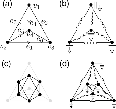
We consider an inductor-capacitor circuit network on a simple directed graph , where and are the sets of vertices and directed edges, respectively. The modifier simple means that there are no multiple edges between any vertex pair and no edge (loop) that connects a vertex to itself. The number of the edges connected to a vertex of a graph is called the degree of . A regular graph is a graph whose every vertex has the same degree. We assume that is an -regular graph with all vertices having degree . The capacitors, all with the same capacitance , are connected between each vertex and the ground. Coils, all with the same inductance , are loaded along all . An example of and the inductor-capacitor circuit network on it are shown in Fig. 1(a) and (b).
For and , the incidence matrix of a directed graph is defined as follows: ( enters ), ( leaves ), otherwise .
Using vector notation, we represent the current distribution flowing along as a column vector . The charge distribution is denoted by with a stored charge at . The charge conservation law is given by
| (1) |
where the time derivative is represented by the dot. The scalar potential at must satisfy Faraday’s law of induction, so we have
| (2) |
with . The scalar potential is written as
| (3) |
with a potential matrix . In our case, is given by
| (4) |
where we use the identity matrix .
with . Assuming , we have an eigenequation
| (5) |
with the Laplacian . We introduce an adjacency matrix , where is 1 if are connected by an edge, otherwise 0. From a direct calculation, we can write by as
| (6) |
where is the degree of the vertex of . Note that is independent of the direction of the edges in because is expressed in terms of and .
The directed graph can be also regarded as an undirected graph. For , we can make an undirected edge , where the bar operator ignores the direction of the edge. Then, we have with . We can also define the undirected incidence matrix as ( and are connected), otherwise . Using , is written as follows Big :
| (7) |
From Eqs. (6) and (7), we obtain
| (8) |
II.2 SUSY correspondence in spectra on a simple regular graph and its line graph
Next, we introduce the line graph concept Big . The line graph of a directed graph is constructed as follows. Each edge in is considered to be a vertex of . Two vertices of are connected if the corresponding edges in have a vertex in common. There are two possible choices for the direction of each edge in and we adapt one of them. From here on, we only consider of a simple -regular graph . In this case, the line graph is a simple -regular graph. The degree can be represented by . For a vertex included in , there are edges connected to . Then, we obtain
| (9) |
Note that is satisfied for a finite graph , where represents the numbers of the elements of the set . Figure 1(c) is an example of the line graph of the graph shown in Fig. 1(a). Figure 1(d) is the inductor-capacitor circuit network on .
In the context of mathematics, it is known that the spectra of the Laplacians for the graph and its line graph are related to each other Shirai (2000). For the convenience of the readers, we rederive this property in a simple manner and apply it to the inductor-capacitor circuit networks. The Laplacian of is written as
| (10) |
with the identity matrix , the incidence matrix , and the adjacency matrix for . The adjacency matrix of is represented as follows Big :
| (11) |
From Eqs. (10) and (11), we have
| (12) |
Now, we consider the composite system of and . Then the composite Laplacian is given by
| (13) |
with
where we have used Eqs. (8), (9), and (12). The composite operator is written as
| (14) |
where the symbol represents the Hermitian conjugate, and we define the supercharge as
These operators satisfy the superalgebra Cooper et al. (1995):
where and are the anticommutator and the commutator, respectively. Therefore, the eigenspectra of the inductor-capacitor circuit networks on the simple regular graph and its line graph must coincide except, possibly, for the highest eigenfrequency. Actually, if we have eigenvector satisfying with the eigenvalue , we obtain , satisfying . Then, we have an eigenvector for when (). The eigenvalue of and must satisfy , because and are positive-semidefinite. For an eigenvector of () with eigenvalue , the partner mode cannot be obtained by multiplying (), because of (). The condition for complete spectral coincidence of the eigenvalues of and is discussed in Appendix A. Note that quantum tight-binding models represented by Eqs. (8) and (12) are isospectral except, possibly, for the highest eigenenergy, but an accurate tuning of the on-site potential satisfying Eqs. (8) and (12) is usually difficult to achieve. The significant point of SUSY for the inductor-capacitor circuit networks is that the on-site potential tuning is accomplished naturally.
If is a periodic graph with lattice vectors , we can show that the spectral coincidence except possibly for the highest eigenfrequency holds for each wave vector. We define parallel translation with as and for edges and vertices, respectively. From the translational symmetry, we have . For a Bloch vector satisfying , we have . This means that is also a Bloch vector. Similar discussion can be applied to . Then, and map Bloch vectors to Bloch vectors without changing . Therefore, the decomposition shown in Eq. (13) is valid in the subspace of Bloch vectors with a wave vector . This means that the spectral coincidence except, possibly, for the highest eigenfrequency holds for each wave vector.
II.3 Examples
II.3.1 finite case
For the graph shown in Fig. 1(a), we have
Then, we get for the inductor-capacitor circuit network on . On the other hand, are obtained for the inductor-capacitor circuit network on . We can see that all angular eigenfrequencies for are included in those for .
II.3.2 Infinite case
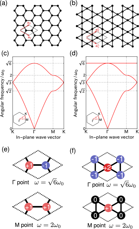
Here, we consider a hexagonal lattice as [Fig. 2(a)]. The line graph is a kagomé lattice [Fig. 2(b)]. To see the spectra coincidence directly, we calculate the angular eigenfrequencies . At first, we calculate the eigenvalue and for and , respectively. Due to the Bloch theorem, it is enough to calculate them in the restricted space of waves with wave vector . For the hexagonal lattice, we have two vertices in a unit cell. The vertex displaced from , with , is denoted by for , where and are lattice vectors for . Now, we define and , where is a complete orthogonal basis of the Hilbert space . The vector subspace is spanned by and . The action of in the restricted space is represented by a matrix , satisfying . Diagonalizing we have
| (15) |
with . By applying a similar calculation to the kagomé lattice, we obtain
| (16) |
with lattice vectors and for . Using Eqs. (5), (6), and (15), we obtain
| (17) |
for the hexagonal lattice. From Eqs. (5), (10), and (16), the kagomé lattice also has the dispersion relation
| (18) |
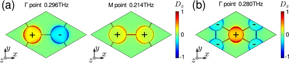
The obtained dispersion relations are shown in Figs. 2(c) and (d). The lower two bands are identical as we expected. Note that these bands are determined only by the product and are independent of the ratio . We also show examples of the eigenmodes for the hexagonal and kagomé lattices in Figs. 2(e) and (f).
III Band correspondence between metallic hexagonal and kagomé lattices
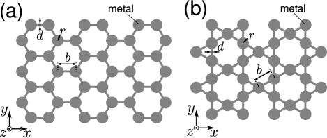
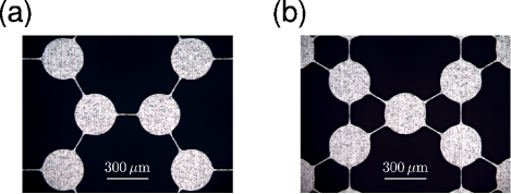
In the previous section, we developed inductor-capacitor circuit networks that are related through SUSY. As an example, we saw that the bands of hexagonal and kagomé inductor-capacitor circuit networks are isospectral by SUSY, except for the highest band of the kagomé lattice. In this section, we examine this correspondence for realistic system. It is known that bar-disk resonators composed of metallic disks connected by metallic bars can be qualitatively modeled by the inductor-capacitor circuit networks discussed in Sec. II, because charges on the disks are coupled dominantly by the current flowing along the bars Nakata et al. (2012b); Kajiwara et al. (2016). The modes on the bar-disk resonators are called spoof plasmons. Here, we study the spoof plasmons of metallic hexagonal and kagomé lattices whose designs are shown in Fig. 3.
III.1 Simulation
We perform an eigenfrequency analysis for the metallic hexagonal and kagomé lattices by the finite element method solver (Comsol Multiphysics). The parameters of the structures for Fig. 3 are as follows: bar width , radius of disks , distance between nearest disks , and thickness . In each simulation, the finite thickness metallic lattice parallel to is located in . The unit cell in the plane is the rhombus spanned by the lattice vectors and denoted by . To reduce the degrees of freedom, we use the mirror symmetry with respect to . A simulation domain with the material parameters of a vacuum is set in with , and a perfect magnetic conductor condition imposed on the surface . Half of the structure in is engraved in the simulation domain and a perfect electric conductor (PEC) boundary condition is imposed on the structure surface. A perfect matched layer (PML) in with a PEC boundary at is used to truncate the infinite effect. The periodic boundary condition with a phase shift (Floquet boundary conditions with a wave vector ) is applied to . Changing along the Brillouin zone boundary, we calculate the eigenfrequencies. To remove the modes which are not localized near the metallic surface Parisi et al. (2012), we select the modes with
where the complex amplitude of the electric field of the mode is denoted by .
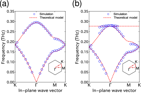
The calculated eigenfrequencies for the metallic hexagonal and kagomé lattices are shown in Fig. 4 as circles. Note that some points are missing because unphysical modes located near PML accidentally exist or couple with the modes. As we explained earlier, we eliminated such modes with . In Fig. 4, we observe the lower two band correspondence between the metallic hexagonal and kagomé lattices. The bands of the metallic hexagonal lattice are about 5% higher than those of the kagomé lattice. However, we can say that the band correspondence is qualitatively established. The detailed theoretical models for fitting curves are discussed later in Appendix. B. Figure 5 shows the electric flux density on of the specific modes, where corresponds to the surface charge on the metal. These mode profiles agree with the theoretically calculated eigenmodes shown in Figs. 2(e) and (f).
III.2 Experiment
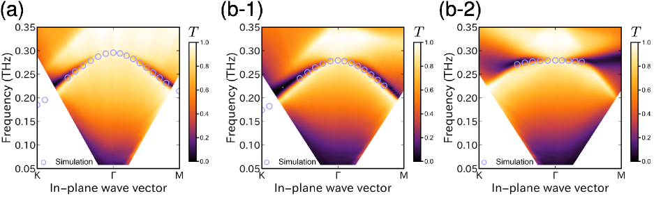
To investigate the dispersion relation experimentally, we fabricated the metallic hexagonal and kagomé lattices by etching and performed transmission measurement on them using the terahertz time-domain spectroscopy technique. The samples made of stainless steel (SUS304) are shown in Fig. 6. The geometrical parameters of these samples are the same as those for the simulation model in Sec. III.1. The area where structures are patterned is . The terahertz beam is generated by a spiral antenna and collimated by a combination of a hyper-hemispherical silicon lens and a Tsurupica lens. The beam diameter is set to by an aperture. Wire-grid polarizers are located near the emitter and detector, which are adjusted so that the emitted and detected fields have the same linear polarization. The transmission spectrum in the frequency domain is obtained from , where and are Fourier transformed electric fields with and without the sample. To scan the Brillouin zone, power transmission spectra are measured with changing incident angle from to with step . Here, the magnitude of the in-plane wave vector is given by , where is the speed of light.
To observe the higher band of the hexagonal lattice and the middle band of the kagomé lattice, the incident waves are set as follows: (i) transverse electric (TE) modes in – scan and (ii) transverse magnetic (TM) modes in – scan. Figures 7(a) and (b-1) show the power transmission spectra for these incident waves entering into the metallic hexagonal and kagomé lattices, respectively. The calculated eigenfrequencies are shown simultaneously as circles in Fig. 7. We can see that the transmission dips form a band from to . The calculated eigenfrequencies are located around the experimental transmission dips. Thus, the SUSY band correspondence for the second band is experimentally demonstrated.
The highest band for the metallic kagomé lattice can be observed for differently polarized incident waves. Figure 7(b-2) shows the transmission spectra for the metallic kagomé lattice, where the incident waves are set as (i) TM modes in the – scan and (ii) TE modes in the – scan. In Fig. 7(b-2), we can see the flat band reported in Ref. Nakata et al., 2012b. Note that the frequencies of the lowest band modes are under the light line, so it is impossible to excite them by free-space plane waves. To excite the lowest band modes, another method, e.g., attenuated total reflection measurement, is needed Kajiwara et al. (2016).
III.3 Discussion
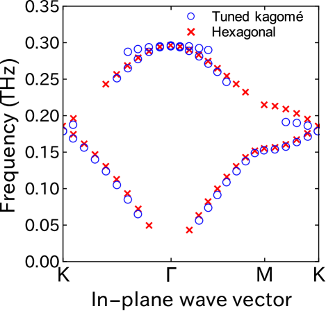
In the previous subsections, the band correspondence between the metallic hexagonal and kagomé lattices was demonstrated, but a discrepancy between the bands was also observed. Here, we investigate the possibility to compensate empirically for the discrepancy. We calculated the eigenfrequencies for the metallic kagomé lattice with the bar width . The other parameters are the same as the previous one. The calculated results are shown in Fig. 8 as circles. To compare with the previous result, the eigenfrequencies for the metallic hexagonal lattice with are also plotted in Fig. 8. We can see the improvement of band correspondence between the metallic hexagonal lattice and tuned metallic kagomé lattice.
IV Conclusion
In this paper, we showed that the inductor-capacitor circuit networks on a simple regular graph and its line graph are related through SUSY, and their spectra must coincide (except possibly for the highest eigenfrequency). The SUSY structure for the circuits was derived from the topological nature of the graphs. To observe SUSY correspondence of the bands in the high frequency range, we investigated the metallic hexagonal and kagomé lattices. The band correspondence between them was predicted by a simulation. We performed terahertz time-domain spectroscopy for these metallic lattices and observed the band correspondence. Finally, we proposed an empirical tuning method to reduce the discrepancy of the corresponding bands of the metallic hexagonal and kagomé lattices.
The theoretical results are formulated for the inductor-capacitor circuit networks and independent of the implementations. Therefore, our results is also applicable to transmission-line systems such as microstrip. The SUSY correspondence in the spectra of inductor-capacitor circuit networks has the potential to extend mode filters Miri et al. (2013a) and mode converters Heinrich et al. (2014a) in two-dimensional (spoof) plasmonic systems.
Acknowledgements.
The present research was supported by the JSPS KAKENHI Grant No. 25790065 and Grant-in-Aid for JSPS Fellows No. 13J04927. Two of the authors (Y. N. and Y. U.) were supported by JSPS Research Fellowships for Young Scientists.Appendix A Condition for complete spectral coincidence of eigenvalues of and
In this Appendix, we consider condition for complete spectral coincidence of the eigenvalues of and . Here, we mainly consider the finite graph cases. At first, we introduce a bipartite graph. A bipartite graph is a graph whose vertex set can be separated into two disjoint sets and such that every edge is connected between a vertex in and that in . Using the concept of a bipartite graph, we obtain the following lemma:
Lemma 1.
Consider a connected graph satisfying and . Let be an undirected incidence matrix of . In this case, is satisfied if and only if is bipartite.
Proof.
:
If the graph is bipartite,
is represented by
the disjoint union of and
as .
The -component row vector of is
denoted by , where
, and
.
Without loss of generality, we can assume
and
.
Because the graph is bipartite,
is satisfied.
:
If we assume ,
| (19) |
is satisfied for and not every . At first we show for all . We assume for . For arbitrary , we consider a path from to , where is the path length, is a function from to satisfying and , and the edge connects vertices and . Considering -column of Eq. (19), we have . Then, we obtain for all . This leads a contradiction because we assumed not every . Therefore, we have for all . We assume , and , without loss of generality. For a given arbitrary , we consider the column component about of Eq. (19). Then, we find is connected between a vertex in and that in . This shows is bipartite. This proof is based on Ref. Van Nuffelen, 1976. ∎
From this lemma, we can prove the following theorem:
Theorem 1.
Consider a simple -regular connected graph with . There exists at least one mode with for the inductor-capacitor circuit network on if and only if is bipartite.
Proof.
Let be an undirected incidence matrix of . is bipartite satisfying satisfying . ∎
On the other hand, we can formulate the condition for presence of eigenvalue of as follows:
Theorem 2.
Consider a simple -regular graph with . There exists at least one mode with for the inductor-capacitor circuit network on if .
Proof.
Let be an undirected incidence matrix of . We have for . Then, satisfying . Finally, satisfying . ∎
From these theorems, all spectra of the inductor-capacitor circuit networks on a simple -regular () connected bipartite graph and its line graph completely coincide. On the other hand, we find that have a non-degenerated eigenvector with eigenvalue for a simple -regular () connected non-bipartite graph (e.g. Sec. II.3.1). For , all spectra of the inductor-capacitor circuit networks on a simple connected -regular graph and its line graph coincide because of . In this case, there are modes if and only if is even.
To analyze an infinite periodic graph with lattice vectors , we take a supercell spanned by , . We impose a periodic boundary condition (called Born–von Karman boundary condition) on the sides of the supercell. Note that this boundary condition just leads to discretization of wave vectors in the Brillouin zone. Now, the infinite graph is reduced to a finite graph and we can use the theorems. For example, the hexagonal lattice is a simple 3-regular connected bipartite graph. Then, the spectra of the inductor-capacitor circuit networks on hexagonal and kagomé lattices include , simultaneously. Note that the spectra of the inductor-capacitor circuit networks on hexagonal and kagomé lattices completely coincide, but their dispersion relations do not.
Appendix B Detailed theoretical model for the metallic hexagonal and kagomé lattices
In this appendix, we derive detailed theoretical models for fitting the eigenfrequencies of the metallic hexagonal and kagomé lattices. For the metallic hexagonal and kagomé lattices, the circuit models treated in Sec. II are approximately valid. To improve the model accuracy, we have to take into account capacitive couplings between disks. Considering only nearest neighboring couplings, we modify Eq. (4) as . Here, represents the capacitive coupling between the adjacent disks Kajiwara et al. (2016). Then, we obtain
for the metallic hexagonal lattice and
for the metallic kagomé lattice. Generally, the coupling constant depends on as , where is the distance between the nearest disks Yeung and Wu (2011). The imaginary part of represents the resistive component. If we only focus on the real part of the eigenfrequencies, we may ignore the resistive term (note that we have already ignored the imaginary part of and ). Then, we assume . Using the real part of the eigenvalues calculated by simulation, we numerically minimize the error
for the hexagonal lattice and
for the kagomé lattice, where we define
The obtained fitting parameters are as follows: , for the hexagonal lattice, and and for the kagomé lattice. Because the magnetic coupling and higher order effects (beyond the nearest capacitive coupling) are included in these parameters, the parameters for the hexagonal and kagomé lattice can be different. The dispersion curves with these fitting parameters are shown in Fig. 4. These curves agree with the simulated data despite the simplicity of the model.
References
- Cooper et al. (1995) F. Cooper, A. Khare, and U. Sukhatme, Phys. Rep. 251, 267 (1995).
- Longhi (2010) S. Longhi, Phys. Rev. A 82, 032111 (2010).
- Longhi and Della Valle (2013a) S. Longhi and G. Della Valle, Ann. Phys. 334, 35 (2013a).
- Longhi and Della Valle (2013b) S. Longhi and G. Della Valle, Europhys. Lett. 102, 40008 (2013b).
- Campo et al. (2014) A. D. Campo, M. G. Boshier, and A. Saxena, Sci. Rep. 4, 5274 (2014).
- Yu et al. (2015) S. Yu, X. Piao, J. Hong, and N. Park, Nat. Commun. 6, 8269 (2015).
- Bernstein and Brown (1984) M. Bernstein and L. S. Brown, Phys. Rev. Lett. 52, 1933 (1984).
- Chumakov and Wolf (1994) S. M. Chumakov and K. B. Wolf, Phys. Lett. A 193, 51 (1994).
- Miri et al. (2013a) M.-A. Miri, M. Heinrich, R. El-Ganainy, and D. N. Christodoulides, Phys. Rev. Lett. 110, 233902 (2013a).
- Laba and Tkachuk (2014) H. P. Laba and V. M. Tkachuk, Phys. Rev. A 89, 033826 (2014).
- Longhi (2015a) S. Longhi, J. Opt. 17, 045803 (2015a).
- Zúñiga-Segundo et al. (2014) A. Zúñiga-Segundo, B. M. Rodríguez-Lara, D. J. Fernández C., and H. M. Moya-Cessa, Opt. Express 22, 987 (2014).
- Miri et al. (2014) M.-A. Miri, M. Heinrich, and D. N. Christodoulides, Optica 1, 89 (2014).
- Longhi (2015b) S. Longhi, Opt. Lett. 40, 463 (2015b).
- Miri et al. (2013b) M.-A. Miri, M. Heinrich, and D. N. Christodoulides, Phys. Rev. A 87, 043819 (2013b).
- Principe et al. (2015) M. Principe, G. Castaldi, M. Consales, A. Cusano, and V. Galdi, Sci. Rep. 5, 8568 (2015).
- Longhi (2014) S. Longhi, Opt. Lett. 39, 1697 (2014).
- Longhi and Della Valle (2014) S. Longhi and G. Della Valle, Phys. Rev. A 89, 052132 (2014).
- Correa et al. (2015) F. Correa, V. Jakubský, and M. S. Plyushchay, Phys. Rev. A 92, 023839 (2015).
- Midya (2014) B. Midya, Phys. Rev. A 89, 032116 (2014).
- Szameit et al. (2011) A. Szameit, F. Dreisow, M. Heinrich, S. Nolte, and A. A. Sukhorukov, Phys. Rev. Lett. 106, 193903 (2011).
- Heinrich et al. (2014a) M. Heinrich, M.-A. Miri, S. Stützer, R. El-Ganainy, S. Nolte, A. Szameit, and D. N. Christodoulides, Nat. Commun. 5, 3698 (2014a).
- Heinrich et al. (2014b) M. Heinrich, M.-A. Miri, S. Stützer, S. Nolte, D. N. Christodoulides, and A. Szameit, Opt. Lett. 39, 6130 (2014b).
- Alexander Maier (2007) S. Alexander Maier, Plasmonics: Fundamentals and Applications (Springer, New York, 2007).
- (25) L. Solymar and E. Shamonina, (Cambridge University Press).
- Nakata et al. (2012a) Y. Nakata, T. Okada, T. Nakanishi, and M. Kitano, Phys. Status Solidi B 249, 2293 (2012a).
- Engheta (2007) N. Engheta, Science 317, 1698 (2007).
- Staffaroni et al. (2012) M. Staffaroni, J. Conway, S. Vedantam, J. Tang, and E. Yablonovitch, Phot. Nano. Fund. Appl. 10, 166 (2012).
- (29) (Cambridge University Press).
- Shirai (2000) T. Shirai, Trans. Am. Math. Soc. 352, 115 (2000).
- Nakata et al. (2012b) Y. Nakata, T. Okada, T. Nakanishi, and M. Kitano, Phys. Rev. B 85, 205128 (2012b).
- Kajiwara et al. (2016) S. Kajiwara, Y. Urade, Y. Nakata, T. Nakanishi, and M. Kitano, Phys. Rev. B 93, 075126 (2016).
- Parisi et al. (2012) G. Parisi, P. Zilio, and F. Romanato, Opt. Express 20, 16690 (2012).
- Van Nuffelen (1976) C. Van Nuffelen, IEEE Trans. Circuits Syst. 23, 572 (1976).
- Yeung and Wu (2011) L. K. Yeung and K.-L. Wu, IEEE Trans. Microwave Theory Tech. 59, 2377 (2011).