Integrated cooling channels in position-sensitive silicon detectors
Abstract
We present an approach to construct position-sensitive silicon detectors with an integrated cooling circuit. Tests on samples demonstrate that a very modest liquid flow very effectively cool the devices up to a power dissipation of over 10 W/cm2. The liquid flow is found to have a negligible impact on the mechanical performance. A finite-element simulation predicts the cooling performance to an accuracy of approximately 10 %.
1 Introduction
Micro-Channel Cooling is used extensively in industry to cool devices with a large power density that are to be employed in areas where the material involved in removing the power must be reduced to the minimum. An obvious application in particle physics are the pixel detectors used in collider experiments to reconstruct the creation vertices and trajectories of charged particles. The requirement of highly granular detectors (and thus large channel density) and fast read-out (requiring larger power in the Front-End) lead to typical power densities of several 100 . At the same time the detector material - and that in supports and services in the detector acceptance - must be reduced to the bare minimum to avoid the effect of multiple scattering on the track parameter resolution. Detector concepts [1] for future electron-positron colliders [2, 3, 4, 5] aim for a total material budget of 0.12-0.2% /layer, where is the radiation length. This is equivalent to only 100-200 of silicon. State-of-the art sensors can be thinned to well below this. One of main challenges is therefore to reduce the material involved in services and supports to below the 0.1% level.
Micro-cooling channels integrated in the detector itself provide a very effective means of removing heat. Bringing the cooling circuit to within hundreds of microns of the heat source and removing thermal barriers (material interfaces, glue layers) reduces the temperature gradient between the heat source and the cooling liquid. The minimal extra material in cooling fluid and circuits helps to reduce the material involved in removing the heat from the detector. Compared to other low-mass proposals (in particular cooling via an air flow in the detector volume) micro-channel cooling is expected to provide a much tighter control over the local temperature.
Several groups have produced micro-cooling circuits in (non-active) silicon wafers for application in high energy physics experiments [6, 7, 8, 9]. Micro-channel cooling is part of the detector concepts for LHCb, NA62 and ALICE. In all these concepts the micro-channel circuit is implemented in a low-mass silicon cooling plate that is brought into thermal contact with the detector that is to be cooled, typically through a thin glue layer.
In this paper we take the integration of cooling and active detector elements one step further by monolithically integrating the micro-channel cooling circuit in a silicon sensor. Our approach fits in a low-pressure, low-mass, mono-phase cooling solution for applications with a relatively modest power density and room-temperature operation, in combination with very strict requirements on the material budget. We validate a production process that combines commercial micro-electronics processing with wafer thinning and the etching of a micro-cooling circuit. We develop a custom connector and a finite element simulation to allow rapid feed-back from laboratory measurement and simulation. Finally, we characterize the thermo-mechanical performance of prototypes.
In Section 2 we present an extension of the process that is used to produce the thin, self-supporting silicon DEPFET sensors for Belle-II [10] and the ILC [11], with an extra step to etch a cooling manifold into the wafer. The custom interface of the micro-channel cooling circuit to commercial high-pressure laboratory equipment is presented in Section 4. Section 5 introduces a finite element simulation of the micro-channel circuit and Section 6 gives an overview of the setup in the laboratory. We present results from a characterization of the local cooling performance of prototypes in Section 7, comparing the laboratory results to a finite-element simulation. The impact on the mechanical stability is reported in Section 8. Finally, the conclusions are presented in Section 9.
2 Integration of the cooling circuit
The approach we follow is based on the silicon-on-insolator thinning concept [12] developed for DEPFET active pixel detectors, the technology chosen for the Belle II vertex detector [10] and a candidate for the linear collider experiments [11]. The process uses two silicon wafers: the top (sensor) wafer forms the active detector material, while the bottom (handle) wafer forms the supporting frame of the all-silicon ladder and, in this implementation, hosts the micro-channel cooling circuit.
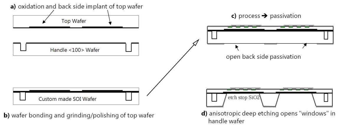
The process is schematically represented in Fig. 1 and can be summarized as follows:
-
•
As the first step both top and handle wafer are thermally oxidized yielding a SiO2 isolation of several 100nm. For sensors requiring an active backside, the backside implantation is done after an optional photolithography step for the definition of the implanted areas.
-
•
A photolithography step on the handle wafer defines the micro-channels. The SiO2 layer is etched acting as a hard mask for the etching dry reactive ion etching (DRIE) of the handle wafer silicon. This DRIE step yields the micro-channels. The typical depth of the channels is a few 100 , determined by the etching time of the DRIE process. In the present case the result of the process are rectangular channels with a depth of about 380 and varying width. After this step, the photoresist and the SiO2 layer are removed.
-
•
After etching the micro-manifold the top and the handle wafer are joined utilizing a direct wafer bonding process. The two wafers are initially held by van-der-Waals forces. After a high-temperature step beyond 1000∘the bond between the wafers is transformed to Si-O-Si bonds. The two wafer wafers are electrically separated by the SiO2 of the top wafer. The top wafer is now thinned down by grinding and a chemical-mechanical polishing (CMP) process to the desired thickness of the sensor material. While this is basically a free parameter, practical considerations (signal-to-noise ratio, mechanical stability) suggest a thickness between 30 and 75 .
-
•
The SOI wafers with integrated cavities in the handle wafer (CSOI) can be processed on a standard semiconductor processing line. In this step the sensor part on the top wafer is finished including the metal layers yielding a fully functional thin sensor material directly bonded to the handle wafer.
-
•
Finally, at the end of the process sequence the oxide at the backside of the handle wafer is opened where the support material is not required. In a wet chemical etching step, the silicon is removed in a Tetramethyl Ammonium Hydroxid (TMAH) solution. The etch process stops at the buried SiO2 layer between handle and top wafer. After cutting the buried micro-channels are exposed and ready to be connected to the cooling circuit.
This process is fully compatible with use of the silicon as the active material in a position-sensitive device. The sensor wafer can be fully depleted through application of a bias voltage. All steps except the insertion of the micro-manifold are identical to the DEPFET manufacturing process for Belle II.
3 Microchannel circuits
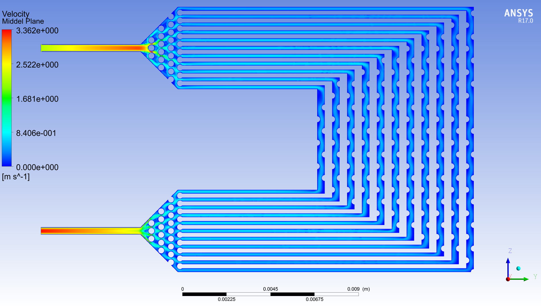
To evaluate the cooling performance of a micro-cooling circuit integrated in the sensor we produced a number of mechanical samples. The design is shown in Figure 2. The inlet and outlet are shown on the leftmost side of the design. Both have a length of 5 mm and an approximately rectangular cross-section of 340 380 . A manifold with multiple cooling lines in parallel is formed by fanning out the inlet in the area. The single channel is divied into 11 separate channels. Circular pillar structures are present in the area to support the thin silicon layer spanning a distance of up to 500 .


The 11 cooling channels have a cross-section of 200 340 (width height). The lengths of the channels vary according to their location; the length of the inner loop is 20 mm, that of the outer loop 40 mm. The expected liquid flow in the manifold is indicated with colours in Figure 2 (the Finite Element simulation used to obtain this information is discussed in Section 5). Clearly, the liquid velocity is highest in the inlet and outlet pipes.
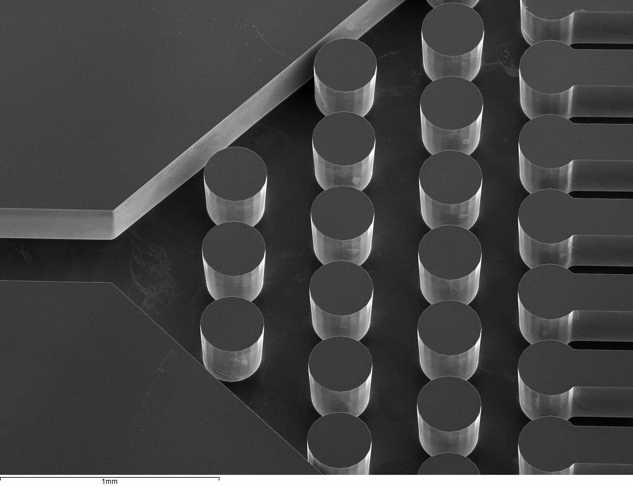
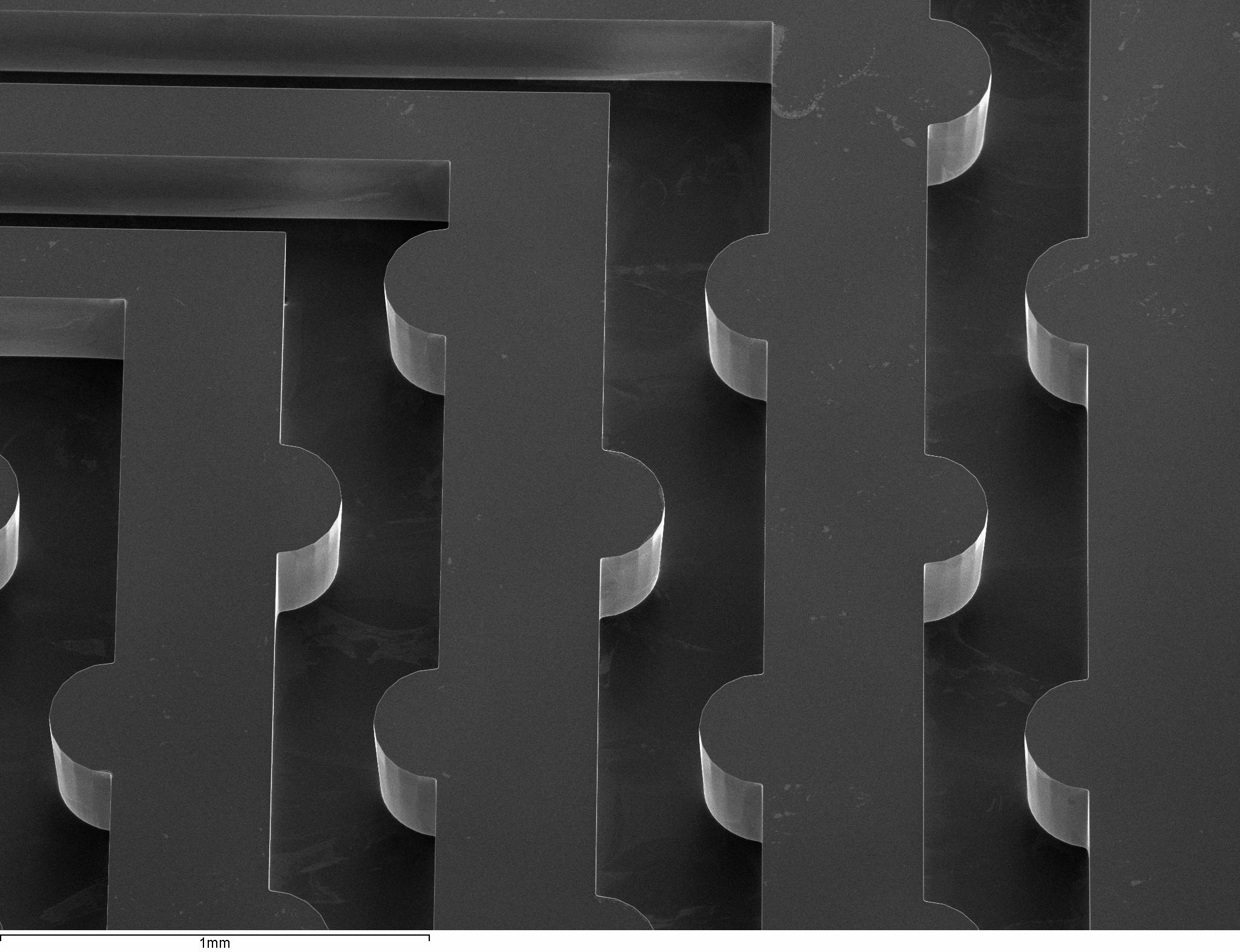
The manifolds are etched into a 450-525 thick silicon handle wafer. The photographs of Figure 3 present two details of the circuit. The photograph on the left zooms in on the position where the inlet (on the left of the image) fans out into several cooling channels. The circular structures are pillars that support the thin layers of silicon covering the triangular area. The photograph on the right shows a detail of several of the corner of four cooling channels. The X-ray images in Figure 3 (c) and (d) present detailed views of the same areas of the circuit after sealing the circuit with the top wafer.
To tackle the connectivity problems and assess the thermo-mechanical performance a small number of test structures was designed and produced for a characterization in the laboratory. The production process follows closely the steps outlined in Section 2, but simplifies the steps not directly related to the thermal performance. The back-side processing mentioned in the first step is omitted. The top-side processing is limited to the implementation of a single metal layer. For these first samples the handle wafer thinning step is not performed222These steps has been performed successfully for a large number of prototypes and are part of the production of the Belle II vertex detector that is in progress at the time of writing.. Figure 4 presents a photograph of these mechanical samples.

These thermo-mechanical samples are equipped with resistive circuits implemented in an Aluminium layer deposited on the surface, that mimic the heat-load from the electronics. Narrow traces are laid out in a serpentine geometry to maximize the length of the trace and thus achieve a resistance of 10-100 . Three independent circuits roughly correspond to the end-of-ladder electronics of the DEPFET ladder design for Belle II (this is where the read-out chips are located; the instantaneous power dissipation is up to 6 W on less than 1 cm2 of the sensor area, as indicated in Fig. 4), the balcony with six steering chips (running along the lower edge of the image) and the sensor itself (the six grey areas that cover the full width of the sensor). The cooling manifold is located exactly under the end-of-ladder heater circuit.
4 Connectors
To connect the micro-channel manifold to a laboratory cooling circuit a custom interface is used that connects the inlet and outlet to standard commercial high-pressure connectors. This connector consists of plastic piece that slides over the silicon sensor, as shown in Fig. 5. The silicon joint is sealed with a glue layer (Araldite2020). On the opposite of the connector there are two threaded holes to connect the standard fittings of the 6 mm outer diameter tubes, visible in the upper right corner of Fig. 5. The channel in the connector gradually reduces the circular cross section of the tube fittings to a square cross section of 400 400 . A photograph through the conical hole is shown in Figure 5.
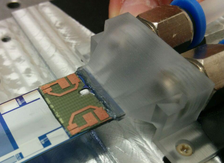
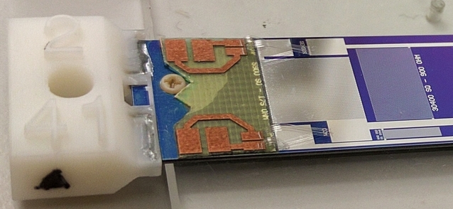
The connectors are produced in a 3D printer using the Stereolithography (SLO) process offered by Sicnova. This technique offers a mechanical precision of 15-30 m (depending of the 3D printing speed) and with thin layers of less than 300 m. The material visijet FX clear with a flexural (tensile) strength of 52 MPa (82 MPa). For such plastic materials the radiation length is typically 35-45 cm.
An assembly consisting of a connector glued onto a silicon sensor was tested for leaks in the CERN micro-channel cooling laboratory. No detectable increase of the Helium level is observed, which allows to put an upper bound on the leak rate. The maximum pressure that the connector stands is 180 bar.
The low- material of the connector has a radiation length of approximately 40 cm. The full thickness of the connectors of the upper panel of Fig. 5 corresponds to 0.8% for a particle crossing under a 90 ∘angle, clearly prohibitive for applications inside the tracking volume of a particle physics experiment. A miniaturized version of the connector has been designed, that offers a reduction of the material by a factor four, while maintaining compatibility with a commercial fitting standard. The result is shown in the lower panel of Figure 5. Even smaller connectors are under development that glue a PEEK micro-tube with a diameter matching that of the micro-channel. These offer a solution with a full thickness equivalent to 0.05% and may be interesting for applications that require the connectors to be in the acceptance. The development of a standard connector for micro-channel cooling is part of Work Package 9 of the AIDA2020 project.
5 Finite element simulation
A finite-element simulation is used to predict the performance of different designs. The geometry presented in Section 3 is implemented in the CFD software Ansys 17.0. The meshed geometry has a total of 4 millions elements, which allow to observe local effects in detail. The cooling fluid in the simulation is pure water and the solid element is silicon. The physical properties of both materials assumed in the simultion are shown in Table 1. The boundary conditions in the simulations - the total power applied to the microchannels and the mass flow - are given in the first two columns of Table 1. They are as close as possible to the laboratory set-up. The environment temperature is set to 25∘, similar to the ambient temperature in the laboratory. The convective heat transfer coefficient used between the sensor and the air is 5 . The temperature of the liquid at the inlet is fixed to 25∘. A power of 6 W is dissipated on the silicon sensor surface immediately above the micro-channel cooling manifold.
| Water | Silicon | |
|---|---|---|
| 997 | 2329 | |
| [J kg-1K-1] | 4181.3 | 713 |
| T [K] | 293 | 293 |
| [W m-1K-1] | 0.58 | 120 |
Results from a number of simulations with varying liquid flow are presented in Table 2. The liquid temperature at the outlet runs several degrees hotter than the inlet side. This reflects the heating of the liquid as it progresses through the manifold. The fourth column in Table 2 presents the simulated outlet temperatures. From these results one can calculate the heat absorbed by the cooling liquid:
| (5.1) |
where is the absorbed power, the liquid mass flow, is the constant pressure heat capacity of the liquid (the value for water is given in table 1) and is the water temperature difference between the inlet and the outlet. The efficiency of the simulated heat exchanger is obtained by comparing the absorbed power with the power absorbed by the liquid flow.
| Dissipated | Liquid mass | Inlet temp. | Outlet temp. | Absorbed | efficiency |
|---|---|---|---|---|---|
| power [W] | flow [kg/s] | Tin [K] | Tout [K] | power [W] | [%] |
| 5.82 | 6.98 | 298 | 315.1 | 5.01 | 86 |
| 5.99 | 9.70 | 298 | 312.0 | 5.69 | 95 |
| 6.12 | 1.29 | 298 | 303.9 | 5.90 | 96 |
| 6.17 | 1.68 | 298 | 306.5 | 5.96 | 97 |
| 6.19 | 2.06 | 298 | 305.0 | 6.01 | 97 |
| 6.21 | 2.42 | 298 | 304.0 | 6.07 | 98 |
| 6.23 | 2.72 | 298 | 303.4 | 6.10 | 98 |
| 6.25 | 3.05 | 298 | 302.8 | 6.14 | 98 |
| 6.25 | 3.45 | 298 | 302.3 | 6.16 | 98 |
| 6.25 | 3.83 | 298 | 301.9 | 6.18 | 99 |
We can now use the simulation to rapidly explore the thermal performance of different designs under conditions that are hard to mimic in the laboratory. As an example we evaluate the effect on the cooling performance of the choice of the coolant. In Fig. 6 the figure-of-merit of several choices are compared. The lower, red curve in Fig. 6 represent the situation of the laboratory measurement in Section 7, where water is used as a coolant. The upper, blue curve in the same figure is obtained when the water is replaced with an alcohol-water mixture (PWG6040).
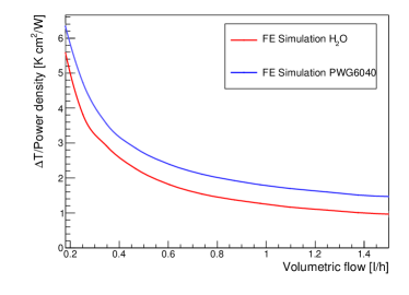
The cooling performance is somewhat degraded for most other choices for the coolant. The temperature gradient found in the simulation is in approximate agreement with a naive scaling by the ratio of heat capacities.
6 Test set-up
In this Section a setup is described to measure the cooling performance of the silicon sensor with embedded micro-channels under a realistic heat load. The aim is to measure the temperature of the sensor surface as a function of the operational parameters, primarily the power consumption and liquid flow. The setup also monitors the position of the sensor to sub- precision.
The measurements are performed deionized water as the cooling fluid. The measurements are representative for any monophase cooling system. In Section 5 we extrapolate to other cooling liquids using the Finite Element simulation. The components to control and monitor the inputs, water flow, pressure and temperature at the inlet and outlet, are presented in Fig. 7.
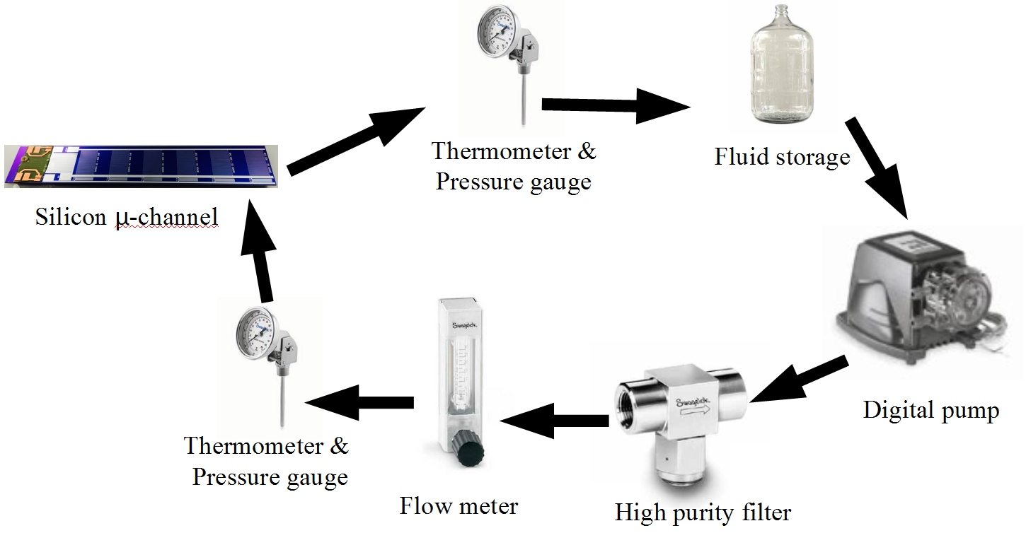
The water flow is established using a digital, variable-speed peristaltic pump (Stenner, SVP1). The flow can be regulated between a fraction of a liter per hour and several liters per hour. The maximum pressure the system can supply is 6 bars. To assure that there are no microparticles which obstruct the microchannels in the silicon ladder, a filter with a maximum particle size of 15 is inserted in the circuit. The liquid flow is measured using a flow meter and temperature sensors and pressure gauges are placed immediately before the inlet and after the outlet of the silicon ladder. All devices use standard SwageLock connectors. The only custom piece is the connector to the micro-channel circuit described in Section 4.
The temperature of the sensor is measured using a thermal infra-red camera (FLIR Systems ThermaCAM SC500) with a field of view that includes the entire surface of the sensor. The temperature readings are calibrated to the readings of sensors in direct contact with the silicon (Pt1000). The contact sensors are only used during calibration runs, so as to avoid any mechanical disturbance. The temperature calibration is applied as a global correction for the average emissitivity of the materials (silicon and aluminium). A more precise reading is obtained with a second single-spot infra-red sensor (Optris CTLaser OPTCTLLTFCF1). This sensor is used to measure the temperature of the hottest point of the silicon ladder.
The mechanical impact of the micro-channel cooling is determined using a triangulating sensor (Micro-Epsilon OptoNCDT ILD2300-10) located above the sensor. This sensor provides readings of the distance to the ladder perpendicular to the sensor surface with a resolution of 0.15 m. The read-out frequency of 1 kHz is sufficient to monitor vibrations in the most important frequency range. To provide maximum sensitivity to deformations and vibrations, the sensor is supported only on one side, by the connector described in Section 4. The distance sensor is placed close to the edge furthest away from the support, for the same reason. The displacement sensor, sensor and support structure are placed on an optical table with pneumatic damping to isolate the system from external vibrations.
7 Thermal performance
The cooling capacity of the micro-manifold integrated in the silicon is characterized in a series of measurements of the maximum temperature on the sensor surface. The measurement is repeated for a number of different settings of the pump speed, corresponding to a liquid flow ranging from a fraction of a liter/hour to 1.5 l/h, and for different values of the power dissipated in the end-of-ladder area. For all measurement the outlet of the cooling circuit is at atmospheric pressure and the ambient temperature between 23-25.
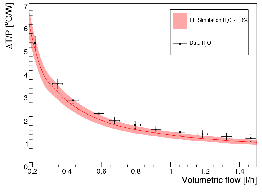
In Figure 8 the temperature gradient from the hottest point on the sensor to the coolant at the inlet of the micro-channel circuit is plotted as a function of liquid flow. The temperature difference is divided by the dissipated power because power is not exactly constant (as the resistance of the heaters on the silicon sensor depends on the temperature).
With a series of measurement at different power the maximum power for a given temperature gradient can be determined. An example is shown in Figure 9, where a maximum gradient of 10 is allowed. At a liquid flow of 3 l/h, the integrated micro-channel circuit removes up to 20 W/ while maintaining the temperature gradient below 10. The curve is nearly linear over the interval of the measurements. While some sign of saturation is visible for the maximum flow rate, the derivative is still two thirds of that at the origin. This implies that the system is still not at its limit: a further increase of the liquid flow can provide further cooling power.
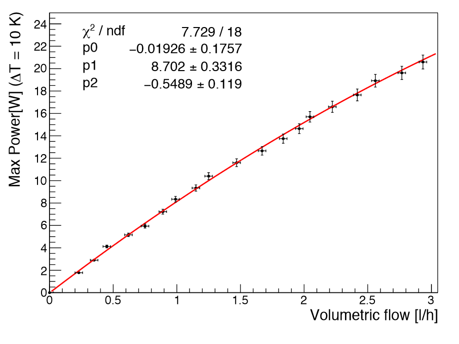
The pressure drop over the micro-channel cooling circuit is 1.5 bar when water flows at 3 l/h. The pressure drop is negligible (below 0.1 bar) at the smallest flow rate of 0.2 l/h.
8 Mechanical impact
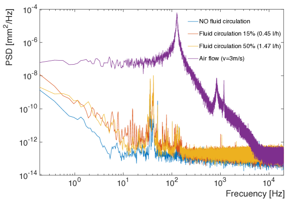
The mechanical stability of the sensor is monitored throughout the measurements. To magnify the deformations the sensor is only supported on one end and the triangulating sensor is located on the opposite end of the ladder. The sensor measures the distance to the ladder. The measurement is therefore sensitive to deformations and vibrations in the direction perpendicular to the sensor area.
Several time series of the distance measurement are recorded under different conditions. The vibrations introduced by the background are measured without liquid flow. The peak-to-peak interval of all distance measurements for this null experiment is less than 0.7 . The Root Mean Square (RMS) of the readings is 0.3. When the measurement is repeated for the maximum liquid flow of 1.47 the excursions increases only very slightly: the peak-to-peak interval is approximately 1 , the RMS increases to 0.4. To check the sensitivity of the setup, the measurements were repeated with an air flow of 3 m/s. This induces a very significant vibrations, with a peak-to-peak interval of 130, demonstrating the sensitivity of the setup to vibrations.
The readings in the time domain are translated to the frequency domain using a fast Fourier transform. The spectral power density if plotted in Fig. 10 for frequencies ranging from a fraction of a Hz to several kHz. The eigenfrequency of the ladder (at 150 Hz) is clearly visible in the spectrum corresponding to the air flow. The other spectra are quite close to the null spectrum, without air or liquid flow. The liquid flow seems to induce very subtle vibrations, with sub- magnitude and frequencies in the 1-100 Hz domain.
9 Conclusions
In this paper we have proposed a process to monolithically integrate a micro-channel cooling circuit in position-sensitive silicon sensors. The process allows to combine standard double-sided processing of the sensor with the precise etching of the cooling manifold and a flexible thinning procedure, while minimizing the number of processing steps with delicate handling of thin structures.
We aim for a low-pressure (several bars), mono-phase cooling solution, with a limited liquid flow, which is adequate in room-temperature applications with modest power consumption. A good example is the tracker and vertex detector of a future energy-frontier collider, but this solution is expected to be applicable in a broad range of application.
A small number of prototype structures has been produced with a channel cross section of 100 380 . The inlet and outlet with an approximately rectangular cross section of 340 380 are accessible from the sensor edge at the narrow end of the silicon ladder. The micro-channel circuit is connected to the main cooling circuit through custom 3D-printed connectors that interface the narrow inlet and outlet to commercial high-pressure connectors. The connection is sealed using Araldite 2011 glue. For the present purpose these plastic structures are found to be sufficiently leak tight. We find they resist a pressure of 180 bars, which is well in excess of the requirement. A future evolution of these connectors could provide a low-Z, low-mass solution in the tracking volume of the experiment.
The cooling performance is measured by applying a power of up to 10 on the surface of the silicon sensor immediately above the integrated cooling circuit. The absence of thermal barriers leads to very efficient evacuation of the dissipated heat. The temperature gradient from the hottest point on the sensor to the liquid can be kept below 2 K for a power density of 6 and a liquid flow of 1 , corresponding to a thermal figure of merit of close to 1.
A finite-element simulation of the cooling circuit is able to reproduce the observed cooling performance, predicting the temperature gradient as a function of liquid flow and power dissipation to within 10%. The simulation is used to simulate a situation, where the power is dissipated on an ASIC that is connected to the sensor through bump bonds. This leads to an increase of the temperature gradient from heat source to heat sink of 5 K.
We find the liquid flow has no significant impact on the mechanical stability of the sensor: the amplitude of vibrations is measured to be smaller than 1, compatible with the null result when no liquid circulates.
Acknowledgement
Part of the funding for the studies reported in this paper stems from the European Union’s Horizon 2020 Research and Innovation programme under Grant Agreement no. 654168. We thank our partners in the AIDA2020 thermo-mechanical work package, and in particular the CERN group (P. Petagna, A. Mapelli, J. Noel) for access to the leak and pressure test.
References
- [1] ILC community Collaboration, The International Linear Collider, Technical Design Rep ort, .
- [2] H. Baer, T. Barklow, K. Fujii, Y. Gao, A. Hoang et. al., The International Linear Collider Technical Design Report - Volume 2: Physics, 1306.6352.
- [3] T. Behnke, J. E. Brau, P. N. Burrows, J. Fuster, M. Peskin et. al., The International Linear Collider Technical Design Report - Volume 4: Detectors, 1306.6329.
- [4] L. Linssen, A. Miyamoto, M. Stanitzki and H. W eerts, Physics and Detectors at CLIC: CLIC Conceptual Design Report, 1202.5940.
- [5] M. Bicer, H. Duran Yildiz, I. Yildiz, G. Coignet, M. Delmastro et. al., First Look at the Physics Case of TLEP, 1308.6176.
- [6] A. Mapelli, P. Petagna, K. Howell, G. Nuessle and P. Renaud, Microfluidic cooling for detectors and electronics, JINST 7 (2012) C01111.
- [7] ALICE Collaboration, B. Abelev et. al., Technical Design Report for the Upgrade of the ALICE Inner Tracking System, J. Phys. G41 (2014) 087002.
- [8] J. Buytaert et. al., Micro channel evaporative cooling for the upgrade of the LHCb vertex detector, Nucl. Instrum. Meth. A731 (2013) 189–193.
- [9] G. Nüssle, A. Mapelli, M. Morel, P. Petagna, G. Romagnoli and K. Howell, NA62 GigaTracKer Cooling with Silicon Micro Channels, in Proceedings, 14th ICATPP Conference on Astroparticle, Particle, Space Physics and Detectors for Physics Applications (ICATPP 2013), pp. 525–530, 2014.
- [10] Belle-II Collaboration, T. Abe et. al., Belle II Technical Design Report, 1011.0352.
- [11] DEPFET Collaboration, O. Alonso et. al., DEPFET active pixel detectors for a future linear collider, 1212.2160.
- [12] L. Andricek, G. Lutz, R. H. Richter and M. Reiche, Processing of ultra-thin silicon sensors for future e+ e- linear collider experiments, IEEE Trans.Nucl.Sci. 51 (2004) 1117–1120.