Unveiling the Penta-Silicene nature of perfectly aligned single and double strand Si-nanoribbons on Ag(110)
From the simplest cyclopentane ring and its numerous organic derivates to their common appearance in extended geometries such as edges or defects in graphene, pentagons are frequently encountered motifs in carbon related systems. Even a penta-graphene Cairo-type two dimensional structure has been proposed as a purely pentagonal C allotrope with outstanding properties competing with those of graphene (cpenta). Conversely, pentagonal Si motifs are hardly found in nature. Despite the large effort devoted to design Si-based structures analogous to those of carbon, the existence of Si pentagonal rings has only been reported in complex clathrate bulk phases (calthrates). Several theoretical studies have hypothesized stable Si pentagonal structures either in the form of one-dimensional (1D) nanotubes (siwires1; siwires2) or at the reconstructed edges of silicene nanoribbons (silicene; silicene1) or even as hydrogenated penta-silicene (pentasilicene) or highly corrugated fivefold coordinated siliconeet (grunberg) 2D sheets, the latter recognized as a topological insulator (heine). However, to date none of them have yet been synthesized. In the present work we unveil, via extended Density functional theory (DFT) (siesta) calculations and Scanning tunneling microscopy (STM) simulations (green; loit), the atomic structure of 1D Si nano-ribbons grown on the Ag(110) surface. Our analysis reveals that this system constitutes the first experimental evidence of a silicon phase solely comprising pentagonal rings.
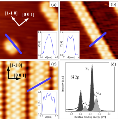
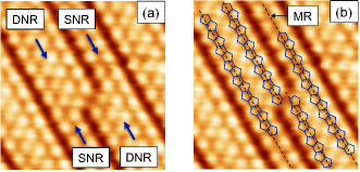
Since their discovery in 2005 (Leandri2005) the atomic structure of Si nano-ribbons (NRs) on Ag(110) has remained elusive and strongly disputed (chinese1; Leandri2005; ronci2010; Lian2012; Borensztein2014; Lagarde2016; arpes1; colonna; chinese). Figure 1 presents a summary of Si NRs measured with STM. The structures were obtained after Si sublimation onto a clean Ag(110) surface at RT. Panels (a) and (b) correspond to a low Si coverage image with an isolated nano-dot structure and a single strand NR (SNR) 0.8 nm wide running along the direction with a 2 periodicity. The SNR topography consists of alternating protrusions at each side of the strand with a glide plane. At higher coverages and after a mild annealing, a dense and highly ordered phase is formed (panel (c)) consisting of double strand NRs (DNRs) with a 5 periodicity along the [001] direction again exhibiting a glide plane along the center of each DNR. The images are in perfect accord with previous works (Leandri2005; ronci2010; colonna; chinese). Further key information on the system is provided by the high-resolution Si- core level photoemission spectrum for the DNRs displayed in Figure 1(d) –that for the SNRs is almost identical (Davila2012). The spectrum can be accurately fitted with only two (spin-orbit splited) components having an intensity ratio of roughly 2:1. Furthermore, previous Angular Resolved Photoemission (ARPES) experiments (Paola2008) assigned the larger and smaller components to subsurface Sis and surface Siad atoms, respectively, indicating that the NRs comprise two different types of Si atoms, with twice as many Sis as Siad.
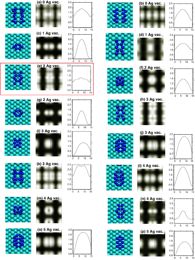
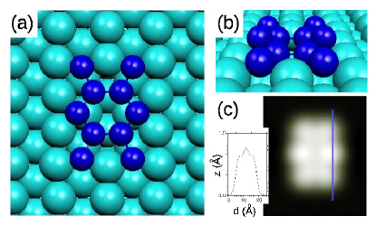
We first focus on the nano-dot shown in Fig. 1(a), as it may be regarded as the precursor structure for the formation of the extended NRs. The nano-dot exhibits a local pmm symmetry with two bright protrusions aligned along the [001] direction, each of them having two adjacent dimmer features along the direction. After considering a large variety of trial models (see ’Extended Data’ Fig 10) we found that only one, shown in Figure 2, correctly reproduces the experimental image both in terms of aspect and overall corrugation. It consists of a ten atom Si cluster located in a double silver vacancy generated by removing two adjacent top row silver atoms. There are four symmetry equivalent Sis atoms residing deeper in the vacancy, two Si in the middle which lean towards short silver bridge sites and four outer Si residing at long bridge sites. The formers lie 0.8 Å above the top Ag atoms and are not resolved in the STM image, while the Si and Si protrude out of the surface by 1.4 and 1.1 Å thus leading to the six bump structure in the simulated image with the Si at the center appearing brighter. Therefore, although the nano-dot shows marked differences with respect to the extended NRs, its structure already accounts for the presence of two distinct types of Si atoms at the surface (Sis and Siad). Furthermore, it reveals the tendency of the Ag(110) surface upon Si adsorption to remove top row silver atoms (i.e. the initial stage in the creation of a missing row (MR)) and incorporate Si nanostructures in the troughs.
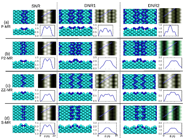
Inspired by the nano-dot Ag di-vacancy structure and by recent grazing incidence X-ray diffraction (XRD) measurements (mr) pointing towards the existence of a MR reconstruction along the direction of the Ag surface, we considered several trial structures for the SNRs by placing Si atoms in the MR troughs (Sis) and next adding further adatoms (Siad) on top, while maintaining a 2:1 concentration ratio between the two. Figures 3(a-b) show top and side views of the optimized geometry for the SNRs after testing several trial models (see ’Extended Data’ Fig. 8). It involves a MR and six Si atoms per cell. The new paradigm is the arrangement of the Si atoms into pentagonal rings running along the MR and alternating their orientation (we denote it as the P-MR model). Despite no symmetry restriction was imposed, the relaxed P-MR SNR belongs to the group presenting two mirror planes plus an additional glide plane along the MR troughs (see ’Extended Data’ Fig. 6 for a detailed description). Apart from a considerable buckling of 0.7 Å between the lower Si atoms residing in the MR troughs (Sis) and the higher ones (Siad) leaning towards short bridge sites at the top silver row, the pentagonal ring may be considered as rather perfect, with a very small dispersion in the Si-Si distances ( Å) and bond angles ranging between ; that is, all close to the in a regular pentagon. The associated STM image and line profile, panel (d), show (symmetry) equivalent protrusions 1.3 Å high at each side of the strand, in perfect agreement with the experimental image. Still, since different models may yield similar STM images, a more conclusive gauge to discriminate among them is to examine their relative formation energies. In this respect, the energetic stability of the P-MR structure is far better ( eV/Si) than all other SNR models considered (see section ’Methods’ and ’Extended Data’ Fig. 9).
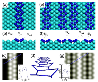
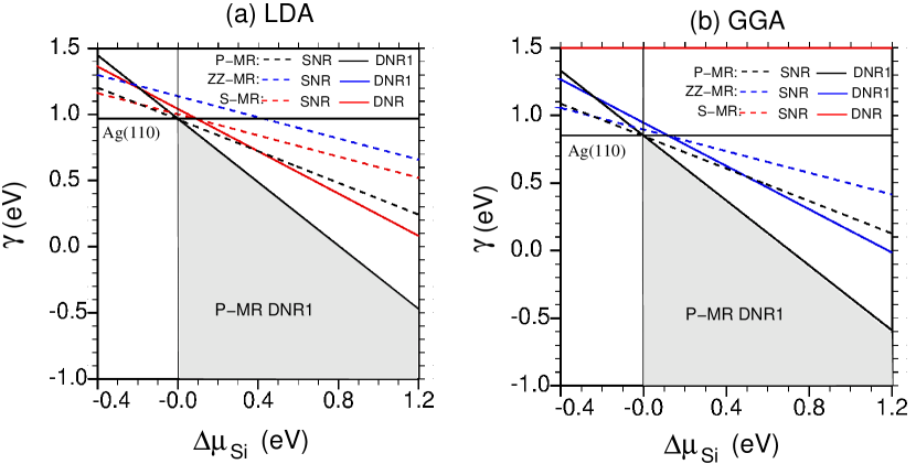
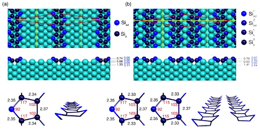
Within the pentagonal model the DNR structure may be naturally generated by placing two SNRs within a cell. However, since the P-MR SNRs are chiral, adjacent pentagonal rings may be placed with the same or with different handedness, leading to two possible arrangements among the enantiomers. Figures 3(e-g) display the optimized geometry and simulated STM topography for the most stable (by 0.03 eV/Si) P-MR DNR configuration. The pentagonal structure in each NR is essentially preserved, the main difference with respect to the SNRs being the loss of the glide plane along the MR troughs replaced by a new one along the top silver row between adjacent SNRs. There is a slight repulsion between the NRs which shifts them away from each other by around 0.2 Å. As a result, the Siad at the outer edges of the DNR end up lying 0.07 Å higher than the inner ones making the alternating pentagons along each strand not strictly equivalent anymore. In the simulated STM image the outer maxima appear dimmer than the inner ones by 0.1 Å, which adopt a zig-zag aspect. The inversion in their relative corrugations is due to the proximity between the inner Si adatoms ( Å) compared to the almost 6 Å distance between the inner and outer ones, so that the bumps of the formers overlap and lead to brighther maxima. All these features are in accordance with the experimental profiles shown in Fig. 1(c). In fact, the P-MR DNR structure is the most stable among all other NR models considered for a wide range of Si chemical potentials ranging from Si-poor to -rich conditions (see ’Extended Data’ Fig. 9).
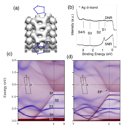
Figure 4 presents a summary of the electronic properties of the P-MR structure. Panel (a) shows an isosurface of the total electronic density for the SNRs. The Sis atoms in the pentagonal rings are clearly linked through an type bonding (three bonds each) while the Siad, due to the buckling, show a distorted type tetrahedral arrangement making bonds with two Sis as well as with the adjacent short bridge silver atoms in the top row. Panel (b) displays ARPES spectra for the SNR and DNR phases. Both energy distribution curves reveal Si-related peaks previously attributed to quantum well states (QWS) originating from the lateral confinement within the NRs.
For the SNRs three states are observed at -1.0, -2.4 and -3.1 eV binding energy (BE), while for the DNRs one further peak is identified at -1.4 eV. The computed (semi-infinite) surface band structures projected on the Si pentagons (blue) and the silver MR surface (red) are superimposed in panels (c) and (d) for the SNRs and DNRs, respectively. Overall, within the expected DFT accuracy and experimental resolution, the maps satisfactorily reproduce the experimental spectra. At the SNRs present two sharp intense Si bands below the Fermi level (S1 and S3) and faint (broader) features arising from two almost degenerate bands (S4 and S5) and a dimmer state (S2). As expected, they are almost flat along while along they present an appreciable dispersion and finally merge into two degenerate states at the high symmetry point. The orbital character of the S2-S5 bands is mainly and may thus be assigned to localized planar bonds. Conversely, band S1 is fully dominated by the Si states (-band) and shows a strong downward dispersion along due to hybridization with the metal bands. Similarly, faint dispersive bands of mainly character hybridizing with the metal appear in the empty states region. The electronic structure for the DNRs is similar to that of the SNRs, except that the number of Si bands is doubled and most of them become splited and shifted due to the interaction between adjacent SNRs. Noteworthy is the appearance of an electron pocket (EP) at associated to a parabolic Si- band with onset at -0.5 eV.
To conclude, we have solved the long debated structure of silicon nano-ribbons on Ag(110), finding an unprecedented 1D penta-silicene phase which consists of adjacent inverted pentagons stabilized within the MR troughs. The model is in accordance with most of previous experimental results for this system: it involves a MR reconstruction as deduced from XRD (mr), comprises two types of Si atoms with a ratio 2:1 between the Sis and Siad concentrations as seen by photoemission, accurately matches the STM topographs also explaining dislocation defects between NRs (see ’Extended Data’ Fig. 7) and accounts for the QWS measured by ARPES. We have also determined the quasi-hexagonal geometry of a Si nano-dot inside a silver-divacancy. This precusor structure for the NRs can be considered as the limiting process for expelling surface Ag atoms in order to create a missing row along which the Si pentagons can develop. We are convinced that the discovery of this novel silicon allotrope will promote the synthesis of analogous exotic Si phases on alternative templates with promising properties (grunberg).
References
Acknowledgements: This work has been funded by the Spanish MINECO under contract Nos. MAT2013-47878-C2-R, MAT2015-66888-C3-1R, CSD2010-00024, MAT2013-41636-P, AYA2012-39832-C02-01/02 and ESP2015-67842-P.
Author contributions: J.I.C. and J.S. performed all the theoretical calculations. A.C.M., M.E.D., and J.M.G.R. performed all the STM experiments. M.E.D. and G.L.L. performed the ARPES measurements. J.I.C. and M.E.D. conceived most of the novel model structures tested. J.I.C. and G.L.L. wrote the manuscript. All authors contributed to the manuscript and figure preparation.
I Methods
Experimental
For both types of prepared structures (isolated Si SNRs or ordered DNRs), the same procedure has been used for sample preparation: i.e. the Ag(110) substrate was cleaned in the Ultra-high vacuum (UHV) chambers (base pressure: 9 mbar) by repeated sputtering of Ar+ ions and subsequent annealing of the substrate at 750 K, while keeping the pressure below 3 mbar during heating. Si was evaporated at a rate of 0.03 ML/min from a silicon source in order to form the NRs. The Ag substrate was kept at room temperature RT to form the isolated SNR 0.8 nm wide, while a mild heating of the Ag substrate at 443 K allows the formation of an ordered grating DNR 1.6 nm wide (Davila2012).
STM measurements were done with a home-made variable temperature UHV STM (Custance2003). All STM data were measured and processed with the WSxM software (Horcas2007). High-Resolution Photoelectron Spectroscopy (HRPEs) experiments of the shallow Si- core-levels and of the valence states, were carried out to probe, comparatively, the structure and the electronic properties of those nanostructures. The ARPES experiments were carried out at the I511 beamline of the Swedish Synchrotron Facility MAX-LAB in Sweden. The end station is equipped with a Scienta R4000 electron spectrometer rotatable around the propagation direction of the synchrotron light. It also houses low energy electron diffraction (LEED) and sputter cleaning set-ups. Further details on the beam line are given in Ref. (Denecke1999). In all the photoemission spectra the binding energy is referenced to the Fermi level. The total experimental resolution for core level and valence band (VB) spectra were 30 meV (h=135.8 eV for Si-) and 20 meV (h=75 eV for the VB), respectively. A least-square fitting procedure was used to analyze the core-levels, with two doublets, each with a spin-orbit splitting of meV and a branching ratio of 0.42. The Si- core level collected at normal emission is dominated by the Sis component. Its full width at half maximum (FWHM) is only 68 meV while the energy difference between the two Sis and Siad components is 0.22 eV.
Theory
All calculations have been carried out at the ab initio level within the Density Functional Theory (DFT) employing the SIESTA-GREEN package (siesta; green). For the exchange-correlation (XC) interaction we considered both the Local Density (ca) (LDA) as well as the Generalized Gradient (pbe) (GGA) approximations. The atomic orbital (AO) basis set consisted of Double-Zeta Polarized (DZP) numerical orbitals strictly localized after setting a confinement energy of 100 meV in the basis set generation process. Real space three-center integrals were computed over 3D-grids with a resolution equivalent to a 700 Rydbergs mesh cut-off. Brillouin zone (BZ) integration was performed over -supercells of around (2028) relative to the Ag-(11) lattice while the temperature in the Fermi-Dirac distribution was set to 100 meV.
All considered Si-NR-Ag(110) structures were relaxed employing two-dimensional periodic slabs involving nine metal layers with the NR adsorbed at the upper side of the slab. A supercell was employed for both the SNR and DNR structures. In all cases, the Si atoms and the first three metallic layers were allowed to relax until forces were below 0.02 eV/Å while the rest of silver layers were held fixed to their bulk positions (for which we used our LDA (GGA) optimized lattice constant of 4.07 Å (4.15 Å), slightly smaller (larger) than the 4.09 Å experimental value).
For the nano-dot calculations, and given that a larger unit cell is required to simulate its isolated geometry, the atomic relaxations of all the trial models (see Fig. 10) were carried out for (45) or (46) supercells. STM topographic images were next computed for all relaxed structures after recomputing the slab Hamiltonians with highly-extended AOs for the surface atoms. Once the correct structure was identified (see Fig. 10), we further optimized it increasing the unit cell to a to remove any overlaps between image cells (see Fig. 2 in the main text).
Band structure– In order to examine the surface band dispersion we computed -resolved surface projected density of states PDOS() maps in a semi-infinite geometry. To this end we stacked the Si-NR and first metallic layers on top of an Ag(110) bulk-like semi-infinite block via Green’s functions matching techniques following the prescription detailed elsewhere (ysi2; loit). For this step we recomputed the slab’s Hamiltonian employing highly extended orbitals (confinement energy of just 10-20 meV) for the Si and Ag surface atoms in the top two layers (this way the spatial extension of the electronic density in the vacuum region is largely extended and the calculation becomes more accurate.
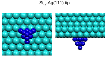
STM simulations– For the STM simulations we modeled the tip as an Ag(111) semi-infinite block with a one-atom terminated pyramid made of ten Si atoms stacked below acting as the apex (see Figure 5). Test calculations employing other tips (e.g. clean Ag or clean W) did not yield any significant changes. Highly extended orbitals were also employed to describe the apex atoms thus reproducing better the expected exponential decay of the current with the tip-sample normal distance . Tip-sample AO interactions were computed at the DFT level employing a slab including the Si NR on top of three silver layers as well as the Si tip apex. The interactions (Hamiltonian matrix elements) were stored for different relative tip-surface positions and next fitted to obtain Slater-Koster parameters that allow a fast and accurate evaluation of these interactions for any tip-sample relative position (loit). Our Green’s function based formalism to simulate STM images includes only the elastic contribution to the current and assumes just one single tunneling process across the STM interface; it has been extensively described in previous works (green; loit). Here we employed an imaginary part of the energy of 20 meV which also corresponds to the resolution used in the energy grid when integrating the transmission coefficient over the bias window. We further assumed the so called wide band limit (WBL) at the tip (loit) in order to alleviate the computational cost and remove undesired tip electronic features. The images were computed at different biases between -2 to +2 V scanning the entire unit cell with a lateral resolution of 0.4 Å always assuming a fixed current of 1 nA. Nevertheless, the aspect of the images hardly changed with the bias, in accordance with most experimental results.
Energetics– To establish the energetic hierarchy among different Si NR structures we first computed their adsorption energies (per Si atom), , via the simple expression:
| (1) |
where are the number of Si and Ag atoms in the slab containing the NR and the Ag(110) surface, refers to its total energy, the energy of the clean Ag surface without the NRs (but including any MRs) and the energy of an isolated Si atom. In the low temperature limit eq. (1) allows to discriminate between structures with the same number of silver and Si atoms.
However, a more correct approach to compare the NR’s stabilities between structures with different Si and Ag concentrations is to compute their formation energies, , as a function of the Si and Ag chemical potentials, . To this end, we employ the standard low temperature expression for the grand-canonical thermodynamic potential (phasediag):
| (2) |
The chemical potentials may be obtained via , where corresponds to the total energy of the isolatad atom and to that of a reference structure acting as a reservoir of Ag or Si atoms. Here we use the bulk phase for silver ( eV and eV), while that of Si is considered as a parameter (see below). The NR’s formation energy, normalized to the Ag(110)- surface unit cell area, then takes the form:
| (3) |
with because the same ) was used for all NR structures and accounts for the formation energy of the unrelaxed surface at the bottom of the slab, which was obtained according to: with giving the total energy of an unrelaxed nine layers thick Ag(110)-(11) slab.
We follow the standard procedure of treating the Si chemical potential as a parameter in eq. (3) and plot the formation energies for each structure as a function of in Figures 9(a) and (b) for the LDA and GGA derived energies, respectively. However, since a reference structure for the Si reservoir is not available (and hence the absolute value of is unknown) we plot the formation energies as a function of a chemical potential shift, , whose origin is placed at the first crossing between the formation energy of the clean Ag(110) and that of any of the NRs (in our case it corresponds to the P-MR DNR structure). Within this somewhat arbitrary choice, small or negative values of would correspond to Si poor conditions, while large positive values to Si rich conditions.
References
| atom | (Å) | (Å) | |
| SNR | Siad | 1.42 | 2.56 (), 2.80 |
| Sis | 0.68 | 2.58, 2.74 | |
| DNR | Si | 1.44 | 2.55 (), 2.87 |
| Si | 1.38 | 2.56 (), 2.78 | |
| Si | 0.68 | 2.58, 2.73 | |
| Si | 0.58 | 2.58, 2.76 |
| Model | SNR | DNR1 () | DNR2 () | ||||||
|---|---|---|---|---|---|---|---|---|---|
| P-MR | 6/88 | 6.44 | 5.70 | 12/86 | 6.43 | 5.70 | 12/86 | 6.40 | 6.57 |
| P2-MR | 6/88 | 6.24 | 5.56 | 12/86 | 6.23 | 5.68 | 12/86 | 6.41 | 5.49 |
| ZZ-MR | 4/88 | 6.36 | 5.59 | 8/86 | 6.35 | 5.58 | 8/86 | 6.34 | 5.58 |
