State-conditional coherent charge qubit oscillations in a Si/SiGe quadruple quantum dot
Abstract
Universal quantum computation requires high fidelity single qubit rotations and controlled two qubit gates. Along with high fidelity single qubit gates, strong efforts have been made in developing robust two qubit logic gates in electrically-gated quantum dot systems to realize a compact and nano-fabrication-compatible architecture. Here, we perform measurements of state-conditional coherent oscillations of a charge qubit. Using a quadruple quantum dot formed in a Si/SiGe heterostructure, we show the first demonstration of coherent two-axis control of a double quantum dot charge qubit in undoped Si/SiGe, performing Larmor and Ramsey oscillation measurements. We extract the strength of the capacitive coupling between double quantum dots by measuring the detuning energy shift ( 75 eV) of one double dot depending on the excess charge configuration of the other double dot. We further demonstrate that the strong capacitive coupling allows fast conditional Landau-Zener-Stuckelberg interferences with conditonal phase flip time about 80 ps, showing promising pathways toward multi-qubit entanglement control in semiconductor quantum dots.
Since being proposed theoretically, Loss:1998p120 ; Kane:1998p133 , much experimental and theoretical progress has been made towards the development of a scalable quantum computing architecture using electrically gated semiconductor quantum dots Hanson:2007p1217 ; Zwanenburg:2013p961 ; Elzerman:2004p431 ; Petta:2005p2180 ; Koppens:2006p766 ; Foletti:2009p903 ; Laird:2010p1985 ; Gaudreau:2011p54 ; Pla:2012p489 ; Medford:2013p654 ; Buch:2013p2017 ; Eng:2015p41 ; Reed:2015unpublished ; Martins:2015unpublished ; Takeda:2016unpublished . Developments in nanofabrication and high fidelity measurement techniques have enabled substantial progress towards realizing two qubit gates in semiconductor quantum dot systems, including the measurement of interqubit capacitive coupling strength Li:2015p7681 , conditional coherent exchange oscillations in GaAs singlet-triplet qubits Shinkai:2009p056802 ; Petersson:2009p016805 ; VanWeperen:2011p030506 , and demonstration of nontrivial entanglement of capacitively coupled GaAs singlet-triplet qubits Shulman:2012p202 . More recently, high fidelity conditional gate operation has been demonstrated in silicon-based quantum dot spin qubits Veldhorst:2014p981 ; Veldhorst:2015p410 , harnessing the substantial improvement in coherence time achieved by isotopic purification of .
Improving gate speed provides an alternative route to realize high fidelity single and multi qubit gates. Intensive efforts to realize fast manipulation of semiconductor spin qubits by mixing the spin degrees of freedom with charge degrees of freedom have been made Petta:2005p2180 ; Wu:2014p11938 ; Berg:2013p066806 ; Medford:2013p654 . Moreover, solely relying on the electric field control, both non-adiabatic coherent control and resonant microwave-driven gate operations have been demonstrated both in GaAs Petersson:2010p246804 ; Cao:2013p1401 ; Cao:2016p086801 and natural Si Shi:2013p075416 ; Kim:2015p243 charge and spin qubits, with typical coherence times of the order of 100 ps to 10 ns. Measured interdot capacitive couplings exceed 20 GHz Li:2015p7681 ; Shinkai:2009p056802 ; Petersson:2009p016805 ; VanWeperen:2011p030506 , so fast multi qubit-gate operations using charge qubits can be expected.
Here, we show fast and charge state conditional coherent manipulation of two strongly coupled double quantum dots. Non-adiabatic pulsed gate techniques allow fast two-axis control of a double dot charge qubit formed in an undoped Si/SiGe heterostructure in the accumulation mode. Furthermore, we show that strong capacitive coupling ( 18 GHz) between two sets of double quantum dots enables charge state conditional coherent Landau-Zener-Stuckelberg interference with a conditional phase flip time about 80 ps, showing promising progress toward realizing high-fidelity two qubit control.
Results
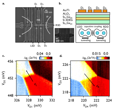
We study a linear quadruple quantum dot formed in an undoped Si/SiGe heterostructure, as shown in Fig. 1a. The dots are formed under the gates through , as shown in Fig. 1b, and for the experiments we report here, it is useful to describe the quadruple quantum dot as a pair of double quantum dots. The right double dot (RDD), formed under the gates and , forms a charge qubit that will be manipulated coherently based on the charge state of the left double dot (LDD), which is formed under gates and . Charge sensing is performed by two charge sensing quantum dots adjacent to the left (LSD) and right (RSD) hand sides of the quadruple dot array. The location of sensor RSD is close to the position that would naively be expected by examination of Fig. 1a; to improve its charge sensitivity, sensor LSD is shifted to a position very close to the quadruple dot by careful tuning of the large number of gate voltages available on that side of the device. We monitor changes in the conductances and of sensor dots LSD and RSD, respectively, to monitor the electron occupations of double dots LDD and RDD. Figures 1c and 1d show charge stability diagrams for LDD (c) and RDD (d), demonstrating control of the four dot occupations as a function of the four gate voltages , , , and . As we show in Supplementary Fig. S1c, the tunnel coupling and the capacitive coupling between the LDD and RDD both become negligible when the LDD is in the few electron regime. Thus, we perform here coherent manipulation in the regime for which the LDD has a total electron occupation larger than (10,10).
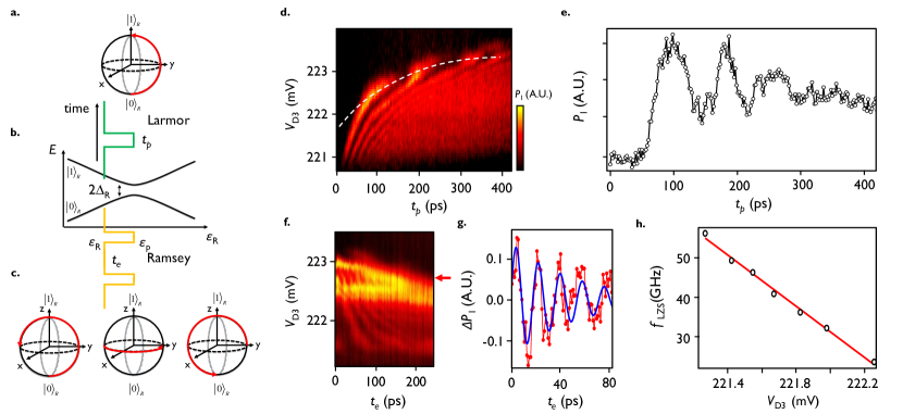
We first show coherent two-axis control of an undoped Si/SiGe double charge qubit formed in the RDD. For this demonstration, the LDD energy detuning is kept 300 eV so that the LDD charge occupation is not affected by the RDD manipulation pulses. The charge qubit states are defined as (excess charge is on the left dot) and (excess charge is on the right dot). The initial qubit state is prepared at negative RDD energy detuning . As shown schematically in Fig. 2a-c, non-adiabatic control of the charge qubit is performed using abrupt changes in detuning energy with precise control of the pulse duration time as well as the amplitude. The pulses, generated using a Tektronix AWG70002A arbitrary waveform generator (AWG) with a rise time of 40 ps, are applied to gate through a commercial bias tee (Picosecond PulseLabs 5542-219). X-rotations on the Bloch sphere, shown in Fig. 2a, correspond to oscillations between the qubit states and . Changing the detuning abruptly to yields an initial state that is a superposition of the eigenstates of the Pauli matrix . At the Hamiltonian is , where is the tunnel coupling between and , so the state evolves periodically in time at the Larmor frequency 2, where is Planck’s constant. After a time evolution of duration , the final state is measured by abruptly changing the detuning back to negative . We use the difference of conductance of the RSD between and to determine a time averaged signal proportional to the probability of the state being in Kim:2014nature .
Figs. 2d and 2e show coherent oscillations of resulting from the non-adiabatic pulse sequences described above. In Fig. 2d we plot as a function of and the gate voltage , the latter of which determines the base level of . In order to overcome a sampling time limitation of our AWG, we modified the pulse generation scheme to allow sub-picosecond timing resolution (see Supplementary Fig. S2). In Fig. 2d, the path of the pulse tip detuning is curved (white dashed curve in Fig. 2d), most likely due to the finite rise time of the pulse and frequency-dependent attenuation in the microwave coaxial cable Petersson:2010p246804 . Fig. 2e shows a line cut through the path corresponding to , revealing periodic oscillations in at a frequency of order 10 GHz, corresponding to GHz. We typically observe beating of the oscillations after = 300 ps. This likely arises because of the superposition of a reflected part of the pulse with the original pulse, modifying the detuning amplitude Petersson:2010p246804 ; Kim:2014nature .
The high frequency oscillations of in Fig. 2d for 222 meV arise from coherent Landau-Zener-Stueckelberg (LZS) interference patterns Shevchenko:2010p1 ; Stehlik:2012p121303 . As becomes less positive in Fig. 2d, the pulse tip detuning enters the regime , where the interdot tunnel coupling acts as a beam splitter Petta:2010p669 ; Shi:2014p3020 . Here, the splitting ratio between the upper and lower branches of the charge qubit dispersion is determined by the detuning ramp rate in comparison with the tunnel coupling. On the return edge of the pulse, the two different trajectories returning through the beamsplitter at can coherently interfere.
The measurement of qubit state rotations about the Z-axis on the Bloch sphere, shown schematically in Fig. 2c, can be performed using two pulses. The qubit state is first prepared in the state , by initializing to state and by performing an rotation. The qubit state then acquires a relative phase , where is the time spent between the two rotations at the base value of the detuning and the qubit energy splitting = . This phase evolution corresponds to a rotation of the qubit state around the Z-axis of the Bloch sphere. Figs. 2f and 2g show the resulting quantum oscillations of the qubit state around the Z-axis of the Bloch sphere. In Fig. 2g, the line cut is taken through mV, corresponding to , and a smooth third order polynomial background oscillation was removed from the raw data for clarity Dovzhenko:2011p161802 ; Shi:2013p075416 (see also Supplementary Fig. S3). By fitting the data to an exponentially damped sinusoidal oscillations, we extract the Ramsey fringe oscillation frequency GHz and a coherence time ps. The gate voltage dependence of both the LZS interference and the Ramsey fringe frequencies provide accurate measures of the detuning lever arm. Fig. 2h shows the LZS oscillation frequency as a function of . As these LZS oscillations are measured in the limit , we use approximate form of the charge qubit energy level, , and fit the data to the form to determine the gate lever arm 32.5 GHz/mV135eV/mV.
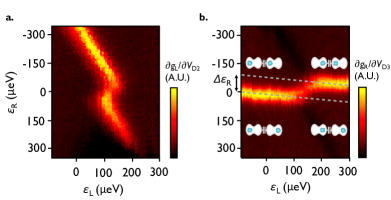
We now discuss the measurement of the capacitive coupling between the double quantum dots. With the detuning lever arm calibrated as described above, along with mutual capacitances between the gates, the coupling strength can be measured by sweeping and through the LDD and RDD charge degeneracy points. Fig. 3 shows the LDD and RDD polarization lines, characterized by measuring the differential conductance of the left and right sensors, LSD (Fig. 3a) and RSD (Fig. 3b), as functions of the two critical variables, the detuning parameters for the LDD and RDD: and . We sweep and by controlling the voltages on (, ) and (, ), respectively. The positions of the excess charges (the electrons in each double dot that are free to move) are shown schematically in the inset to Fig. 3b. The coupled charge stability diagram reveals the four possible ground state charge configurations for an extra electron in each of the two double dots. The gray dashed lines in Fig. 3b show the RDD detuning energy shift () arising from the movement of a single electron from left to right in the LDD. The shift in this line is a direct measure of the energy shift in the RDD resulting from the capacitive coupling between the two double dots. From the energy calibrations reported above, we extract 75 eV 18.3 GHz. This energy shift is the available detuning modulation for the performance of two-qubit gates in quantum dots of a size and separation similar to those studied here.
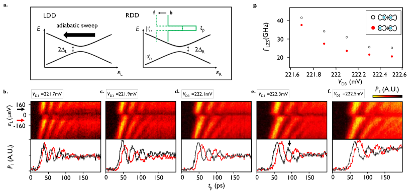
We now show that the capacitive coupling demonstrated above enables fast charge-state-conditional phase evolution of a quantum dot charge qubit. We study LZS oscillations in the RDD in the presence of a perturbation from the excess charge in the LDD. Fig. 4a illustrates schematically the pulse sequence used for this experiment. The base detuning for the short pulse, shown in green in Fig. 4a, is controlled using , and in Figs. 4b to 4f, we vary from to in steps of 0.2 mV. The effect of these steps is to change the energy in detuning of the tip of the fast pulse, thus changing the frequency of the LZS oscillations. For each of these LZS oscillation measurements, is swept from +180 to -320 eV (the vertical axis in Figs. 4b-f), in order to change the excess charge occupation of the left double dot from to — this change occurs quite abruptly at zero detuning of the LDD, as can be observed in Figs. 4b-f. The interference pattern shows two characteristic features as a function of . First, there is a continuous and gradual increase in frequency as a function of , arising from the capacitive coupling between the gates above LDD and the RDD. In addition, there is a sudden decrease in frequency in Figs. 4b to 4f as takes the LDD from positive to negative detuning. This decrease in frequency reflects the decreased that the LZS pulse tip reaches, because of the effective change in baseline detuning energy arising from the one electron charge transition in the LDD. The bottom panels of Figs. 4b to 4f show line cuts of the LZS oscillations in the RDD for the LDD ground state (black) and LDD ground state (red, see black and red arrows in Fig. 4b). Clearly a phase change arises from the motion of one electron in the LDD, and we achieve a conditional phase flip in a time as short as 80 ps, as indicated by the black arrow in Fig. 4e. Fig. 4g shows the difference in between the cases when the LDD ground state is (black circles) and when this ground state is (red circles). This difference in frequency ranges from 7 to 10 GHz and can be used to infer the speed of a conditional phase (CPHASE) gate if full control over qubits in both the left and right double dots is realized in the future. We emphasize that the frequency changes observed here arise from competing effects; of the RDD increases as we change a gate voltage to increase , whereas decreases as we cross zero detuning in the LDD, resulting in the motion of a single electron charge. Since we take line cuts at 80 eV to clearly show LZS oscillations in the and ground states, we believe that using LDD detuning pulse amplitude 160eV, when LDD coherent manipulation is realized, can lead to a faster conditional phase gate than estimated here.
Discussion
Using strong capacitive coupling between two double quantum dots in a linear quad dot array geometry (18 GHz), we achieve fast charge state conditional coherent oscillations with a conditional phase flip time of 80 ps, demonstrating the key physical interaction necessary for a two-qubit CPHASE gate. Moreover, because we measure single qubit X (Larmor) and Z (Ramsey) rotations with rotation frequencies also on the order of 10 GHz, one can envision fast universal quantum logic gates in semiconductor charge qubits. Resonant microwave control is also plausible Kim:2015p243 , in which case a two-qubit controlled not gate (CNOT) can be implemented Li:2015p7681 ; Veldhorst:2015p410 . We stress however that the full demonstration of two qubit gates remains as a challenge, as in this work coherent control of the LDD could not be achieved. A more compact gate geometry, for example, using an overlapped Al/ gate structure Veldhorst:2014p981 ; Zajac:2015p223507 can be considered, in order to allow tunability as well as strong confinement and large tunnel coupling strength down to the single electron regime.
Methods
Fabrication: The device heterostructure was grown using chemical vapor deposition (CVD) on commercially available SiGe substrates with a 29% Ge composition. The CVD growth sequence from the starting substrate was deposition of a strain-matched SiGe buffer layer followed by deposition of a 12 nm thick strained Si well. The well was capped by deposition of a 50 nm of SiGe, followed by a few nanometers of sacrificial strained Si to cap the heterostructure.
Devices were fabricated using a combination of electron beam lithography (EBL) and photolithography. The device nanostructure was fabricated in two layers starting on a 15 nm gate dielectric of deposited by atomic layer deposition (ALD). The first layer of control gates was patterned in two EBL/metallization steps to improve the gate density and metallized with Ti/Au. The second reservoir gate layer (see inset to Fig. 1a) is isolated from the first with another 80 nm layer of grown via ALD. The second gate layer was also metallized with Ti/Au. A third layer of was deposited over the second gate layer to protect the gates during subsequent fabrication steps. Ohmic contacts were fabricated using annealed P+ ion implants.
Measurement: The charge stability diagrams of the LDD and RDD are characterized by measuring the conductance changes through the left and right sensor dots (LSD and RSD respectively, see Fig. 1a), which are operated at a fixed voltage bias of 50 V, and the currents are measured with two current preamplifiers (DL Instruments model 1211). Supplementary Fig. S1 provides large scale charge stability diagrams and the positions of charge transitions of the LDD and RDD in the few electron regime used in the present experiment. For the manipulation of the RDD charge qubit, fast voltage pulses with repetition rate of 25 MHz are generated using two channel outputs of a Tektronix AWG70002A arbitrary waveform generator and are added to the dot-defining dc voltage through a bias tee (Picosecond Pulselabs 5546-107) before being applied to gate . The conductance change through the right sensor dot (RSD) with and without the manipulation pulses, measured with a lock-in amplifier (EG&G model 7265), is used to determine the average charge occupation and is converted to the probabilities. For the measurement of changes in charge occupation probabilities resulting from fast manipulation pulses, we modulated the manipulation pulses with a low frequency (777 Hz) square wave envelope, similar to the technique we used in previous studies Kim:2015p243 ; Kim:2015p15004 . We compare the measured signal level with the corresponding to charge transition signal level, calibrated by sweeping gate and applying a 777 Hz square pulse to gate D3 with an amplitude the same as the manipulation pulses.
Acknowledgements
This work was supported in part by ARO (W911NF-12-0607), NSF (DMR-1206915, PHY-1104660), ONR (N00014-15-1-0029), and the Department of Defense. The views and conclusions contained in this document are those of the authors and should not be interpreted as representing the official policies, either expressly or implied, of the US Government. Work also supported by the Laboratory Directed Research and Development program at Sandia National Laboratories. Sandia National Laboratories is a multi-program laboratory managed and operated by Sandia Corporation, a wholly owned subsidiary of Lockheed Martin Corporation, for the U.S. Department of Energy’s National Nuclear Security Administration under contract DE-AC04-94AL85000. Development and maintenance of the growth facilities used for fabricating samples is supported by DOE (DE-FG02-03ER46028). This research utilized NSF-supported shared facilities at the University of Wisconsin-Madison.
Author Contributions
DRW fabricated the quantum dot device and developed hardware and software for the measurements. DK performed electrical measurements with RHF and analyzed the data with MAE, MF, and SNC. DES and MGL prepared the Si/SiGe heterostructure. All authors contributed to the preparation of the manuscript.
Additional Information
Supplementary information accompanies this paper. Correspondence and requests for materials should be addressed to Mark A. Eriksson (maeriksson@wisc.edu)
Supplementary Information
SUPPLEMENTARY NOTE 1 Charge stability measurements
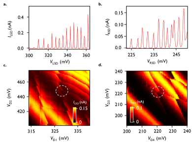
For measuring changes in charge occupation and charge qubit probabilities, we use two single electron transistors formed on the left and right hand side of the linear quadruple dot array (see Fig. 1a - LSD and RSD in the main text). Supplementary Figs. 1a and 1b show Coulomb blockade peaks of the charge sensors. By adjusting and to be near maxima of the current through LSD and RSD, the charge occupation in the and ( and ) double dot can be measured using (). Supplementary Figs.1c and 1d show the large scale charge stability diagrams of the left double dot (LDD, 1c) and right double dot (RDD,1d), respectively. We find that both the tunnel coupling strength and the inter-double dot capacitive coupling becomes negligible as electrons are removed from the LDD as it can be inferred from the trend of the polarization lines in Supplementary Fig.1c, whereas the tunnel coupling of the RDD can be maintained 10 GHz down to few electron regime. Thus we choose the LDD electron occupation number to be in the regime (10, 10). The regions of the charge stability diagrams used for the pulse experiments are denoted as white dashed circles in the Supplementary Figs. 1c and 1d.
SUPPLEMENTARY NOTE 2 Pulse generation and probability measurement details
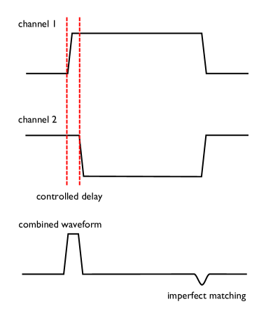
Manipulation pulse sequences are generated using a Tektronix AWG70002A arbitrary waveform generator (AWG). The minimum sampling time of 40 ps typically results in timing resolution that is not adequate to measure 10 GHz oscillations. To increase timing resolution, we use both channel outputs of the AWG as shown in Supplementary Figure 2. In this approach, channel one outputs a 10 ns duration pulse and channel two outputs an opposite polarity pulse delayed by desired pulse width , which is controlled by an analog skew control with timing resolution better than 1 ps. As the channel output is delayed, a short pulse with opposite polarity appears at about 10 ns due to imperfect cancellation of pulse end edges. Since this opposite pulse is in the measurement step, it does not induce charge transitions. In order to keep the duration of this unwanted mismatch as short as possible, we adjust the total pulse duration of the channel to be 10 ns - rounded to nearest multiple of 40 ps.
In order to measure the charge qubit state probability, we adopt the general scheme described in our previous studies, where we measure the difference between the RSD conductance with and without the manipulation pulses Kim:2014nature ; Kim:2015p243 . The data are acquired using a lock-in amplifier with a reference signal corresponding to the presence and absence of the pulses (lock-in frequency 777 Hz). We compare the measured signal level with the corresponding - charge transition signal level, calibrated by sweeping gate and applying square square pulses with frequency of 777 Hz to gate .
SUPPLEMENTARY NOTE 3 Background removal in the Ramsey fringe data
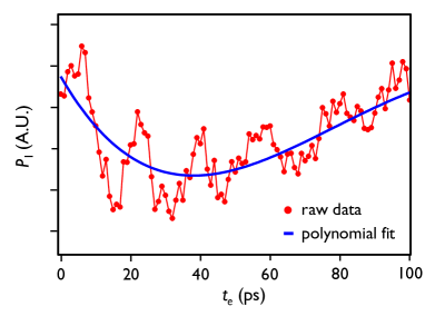
Supplementary Fig. S3 shows the raw oscillation data corresponding to a Ramsey fringe measurement using two pulses. The data typically show a smooth background variation in the measured probability, as shown in Supplementary Fig. S3. This background is likely due to frequency dependent attenuation and inexact calibration of the state initialization and measurement pulse durations limited by sampling time of the AWG. When we analyze the data to extract the inhomogeneous coherence time *, we fit the background to third order polynomial (blue solid curve in Supplementary Fig. S3) and subtract this polynomial from the raw data. The resultant high frequency oscillations are shown in Fig. 2g in the main text.
SUPPLEMENTARY NOTE 4 Charge state dependent Larmor oscillations
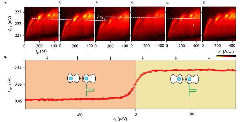
In the main text, we showed a coherent interference pattern with fixed RDD energy detuning as the LDD energy detuning is swept. Here we show the interference pattern as a function of with fixed. Supplementary Figs. 4a-f shows RDD Larmor oscillation patterns as a function of and pulse tip duration as the LDD detuning energy is varied from -100 (a) to +100 eV (f). As is changed, the overall coherent oscillation pattern shifts due to mutual capacitance between the gates. However, we find that the Larmor oscillation frequency of about 10 GHz is roughly constant from a to f. The effect of the LDD charge transition is evident when c and d are compared, where the strong capacitive coupling results in a sudden shift of the pattern in the opposite direction (see in Supplementary Fig. 4c). The origin of this shift is supported by simultaneously measured (g) as a function of , showing that the charge transition indeed occurs in the LDD from c to d, providing evidence that the change in interference pattern frequency measured in the main text is due to a single electron transition.
References
- (1) Loss, D. & DiVincenzo, D. P. Quantum computation with quantum dots. Phys. Rev. A 57, 120–126 (1998).
- (2) Kane, B. E. A silicon-based nuclear spin quantum computer. Nature 393, 133–137 (1998).
- (3) Hanson, R., Kouwenhoven, L. P., Petta, J. R., Tarucha, S. & Vandersypen, L. M. K. Spins in few-electron quantum dots. Rev. Mod. Phys. 79, 1217–1265 (2007).
- (4) Zwanenburg, F. A., Dzurak, A. S., Morello, A., Simmons, M. Y., Hollenberg, L. C. L., Klimeck, G. et al. Silicon quantum electronics. Rev. Mod. Phys. 85, 961 (2013).
- (5) Elzerman, J. M., Hanson, R., Willems van Beveren, L. H., Witkamp, B., Vandersypen, L. M. K. & Kouwenhoven, L. P. Single-shot read-out of an individual electron spin in a quantum dot. Nature 430, 431–435 (2004).
- (6) Petta, J. R., Johnson, A. C., Taylor, J. M., Laird, E. A., Yacoby, A., Lukin, M. D. et al. Coherent manipulation of coupled electron spins in semiconductor quantum dots. Science 309, 2180–2184 (2005).
- (7) Koppens, F. H. L., Buizert, C., Tielrooij, K. J., Vink, I. T., Nowack, K. C., Meunier, T. et al. Driven coherent oscillations of a single electron spin in a quantum dot. Nature 442, 766–771 (2006).
- (8) Foletti, S., Bluhm, H., Mahalu, D., Umansky, V. & Yacoby, A. Universal quantum control of two-electron spin quantum bits using dynamic nuclear polarization. Nature Physics 5, 903–908 (2009).
- (9) Laird, E. A., Taylor, J. M., DiVincenzo, D. P., Marcus, C. M., Hanson, M. P. & Gossard, A. C. Coherent spin manipulation in an exchange-only qubit. Phys. Rev. B 82, 075403 (2010).
- (10) Gaudreau, L., Granger, G., Kam, A., Aers, G. C., Studenikin, S. A., Zawadzki, P. et al. Coherent control of three-spin states in a triple quantum dot. Nature Phys. 8, 54–58 (2011).
- (11) Pla, J. J., Tan, K. Y., Dehollain, J. P., Lim, W. H., Morton, J. J. L., Jamieson, D. N. et al. A single-atom electron spin qubit in silicon. Nature 489, 541–545 (2012).
- (12) Medford, J., Beil, J., Taylor, J. M., Bartlett, S. D., Doherty, A. C., Rashba, E. I. et al. Self-consistent measurement and state tomography of an exchange-only spin qubit. Nature Nanotech. 8, 654–659 (2013).
- (13) Buch, H., Mahapatra, S., Rahman, R., Morello, A. & Simmons, M. Y. Spin readout and addressability of phosphorus-donor clusters in silicon. Nature Comm. 4, 2017 (2013).
- (14) Eng, K., Ladd, T. D., Smith, A., Borselli, M. G., Kiselev, A. A., Fong, B. H. et al. Isotopically enhanced triple-quantum-dot qubit. Sci. Adv. 1 (2015).
- (15) Reed, M., Maune, B., Andrews, R., Borselli, M., Eng, K., Jura, M. et al. Reduced sensitivity to charge noise in semiconductor spin qubits via symmetric operation. arXiv preprint arXiv:1508.01223 (2015).
- (16) Martins, F., Malinowski, F. K., Nissen, P. D., Barnes, E., Fallahi, S., Gardner, G. C. et al. Noise suppression using symmetric exchange gates in spin qubits. arXiv preprint arXiv:1511.07336 (2015).
- (17) Takeda, K., Kamioka, J., Otsuka, T., Yoneda, J., Nakajima, T., Delbecq, M. et al. A fault-tolerant addressable spin qubit in a natural silicon quantum dot. arXiv preprint arXiv:1602.07833 (2016).
- (18) Li, H.-O., Cao, G., Yu, G.-D., Xiao, M., Guo, G.-C., Jiang, H.-W. et al. Conditional rotation of two strongly coupled semiconductor charge qubits. Nature Comm. 6 (2015).
- (19) Shinkai, G., Hayashi, T., Ota, T. & Fujisawa, T. Correlated coherent oscillations in coupled semiconductor charge qubits. Phys. Rev. Lett. 103, 056802 (2009).
- (20) Petersson, K., Smith, C., Anderson, D., Atkinson, P., Jones, G. & Ritchie, D. Microwave-driven transitions in two coupled semiconductor charge qubits. Phys. Rev. Lett. 103, 016805 (2009).
- (21) Van Weperen, I., Armstrong, B., Laird, E., Medford, J., Marcus, C., Hanson, M. et al. Charge-state conditional operation of a spin qubit. Phys. Rev. Lett. 107, 030506 (2011).
- (22) Shulman, M. D., Dial, O. E., Harvey, S. P., Bluhm, H., Umansky, V. & Yacoby, A. Demonstration of entanglement of electrostatically coupled singlet-triplet qubits. Science 336, 202–205 (2012).
- (23) Veldhorst, M., Hwang, J. C. C., Yang, C. H., Leenstra, A. W., de Ronde, B., Dehollain, J. P. et al. An addressable quantum dot qubit with fault-tolerant control-fidelity. Nature Nanotech. 9, 981–985 (2014).
- (24) Veldhorst, M., Yang, C. H., Hwang, J. C. C., Huang, W., Dehollain, J. P., Muhonen, J. T. et al. A two-qubit logic gate in silicon. Nature 526, 410 (2015).
- (25) Wu, X., Ward, D. R., Prance, J. R., Kim, D., Gamble, J. K., Mohr, R. T. et al. Two-axis control of singlet-triplet qubit with an integrated micromagnet. Proc. Nat. Acad. Sci. USA 111, 11938 (2014).
- (26) van den Berg, J. W. G., Nadj-Perge, S., Pribiag, V. S., Plissard, S. R., Bakkers, E. P. A. M., Frolov, S. M. et al. Fast spin-orbit qubit in an indium antimonide nanowire. Phys. Rev. Lett. 110, 066806 (2013).
- (27) Petersson, K. D., Petta, J. R., Lu, H. & Gossard, A. C. Quantum coherence in a one-electron semiconductor charge qubit. Phys. Rev. Lett. 105, 246804 (2010).
- (28) Cao, G., Li, H.-O., Tu, T., Wang, L., Zhou, C., Xiao, M. et al. Ultrafast universal quantum control of a quantum-dot charge qubit using Landau–Zener–Stückelberg interference. Nature Comm. 4, 1401 (2013).
- (29) Cao, G., Li, H.-O., Yu, G.-D., Wang, B.-C., Chen, B.-B., Song, X.-X. et al. Tunable hybrid qubit in a gaas double quantum dot. Phys. Rev. Lett. 116 (2016).
- (30) Shi, Z., Simmons, C. B., Ward, D. R., Prance, J. R., Koh, T. S., Gamble, J. K. et al. Coherent quantum oscillations and echo measurements of a si charge qubit. Phys. Rev. B 88, 075416 (2013).
- (31) Kim, D., Ward, D. R., Simmons, C. B., Gamble, J. K., Blume-Kohout, R., Nielsen, E. et al. Microwave-driven coherent operations of a semiconductor quantum dot charge qubit. Nature Nanotech. 10, 243–247 (2015).
- (32) Kim, D., Shi, Z., Simmons, C., Ward, D., Prance, J., Koh, T. S. et al. Quantum control and process tomography of a semiconductor quantum dot hybrid qubit. Nature 511, 70–74 (2014).
- (33) Shevchenko, S. N., Ashhab, S. & Nori, F. Landau–Zener–Stückelberg interferometry. Physics Reports 492, 1–30 (2010).
- (34) Stehlik, J., Dovzhenko, Y., Petta, J. R., Johansson, J. R., Nori, F., Lu, H. et al. Landau-Zener-Stückelberg interferometry of a single electron charge qubit. Phys. Rev. B 86, 121303 (2012).
- (35) Petta, J. R., Lu, H. & Gossard, A. C. A coherent beam splitter for electronic spin states. Science 327, 669–672 (2010).
- (36) Shi, Z., Simmons, C. B., Ward, D. R., Prance, J. R., Wu, X., Koh, T. S. et al. Fast coherent manipulation of three-electron states in a double quantum dot. Nature Comm. 5, 3020 (2014).
- (37) Dovzhenko, Y., Stehlik, J., Petersson, K. D., Petta, J. R., Lu, H. & Gossard, A. C. Nonadiabatic quantum control of a semiconductor charge qubit. Phys. Rev. B 84, 161302 (2011).
- (38) Zajac, D. M., Hazard, T. M., Mi, X., Wang, K. & Petta, J. R. A reconfigurable gate architecture for Si/SiGe quantum dots. Appl. Phys. Lett. 106, 223507 (2015). arXiv:eprint 1502.01624.
- (39) Kim, D., Ward, D. R., Simmons, C. B., Savage, D. E., Lagally, M. G., Friesen, M. et al. High-fidelity resonant gating of a silicon-based quantum dot hybrid qubit. npj. Quant. Inf. 1 (2015).