Three-Axis Vector Nano Superconducting Quantum Interference Device
Abstract
We present the design, realization and performance of a three-axis vector nano Superconducting QUantum Interference Device (nanoSQUID). It consists of three mutually orthogonal SQUID nanoloops that allow distinguishing the three components of the vector magnetic moment of individual nanoparticles placed at a specific position. The device is based on Nb/HfTi/Nb Josephson junctions and exhibits linewidths of nm and inner loop areas of nm2 and nm2. Operation at temperature K, under external magnetic fields perpendicular to the substrate plane up to mT is demonstrated. The experimental flux noise below in the white noise limit and the reduced dimensions lead to a total calculated spin sensitivity of and for the in-plane and out-of-plane components of the vector magnetic moment, respectively. The potential of the device for studying three-dimensional properties of individual nanomagnets is discussed.
I Introduction
Getting access to the magnetic properties of individual magnetic nanoparticles (MNPs) poses enormous technological challenges. As a reward, one does not have to cope with troublesome inter-particle interactions or size-dependent dispersion effects, which facilitates enormously the interpretation of experimental results. Moreover, single particle measurements give direct access to anisotropy properties of MNPs, which are hidden for measurements on ensembles of particles with randomly distributed orientation.Martínez-Pérez et al. (2010); Silva et al. (2005)
So far, different techniques have been developed and successfully applied to the investigation of individual MNPs or small local field sources in general. Most of these approaches rely on sensing the local stray magnetic field created by the sample under study, by using e.g., micro- or nanoSQUIDs,Granata and Vettoliere (2016); Schwarz et al. (2015); Buchter et al. (2015); Shibata et al. (2015); Schmelz et al. (2015); Vasyukov et al. (2013); Arpaia et al. (2014); Hazra et al. (2014); Wölbing et al. (2013); Levenson-Falk et al. (2013); Buchter et al. (2013); Bellido et al. (2013); Granata et al. (2013); Martínez-Pérez et al. (2011); Hao et al. (2011); Kirtley (2010); Giazotto et al. (2010); Vohralik and Lam (2009); Huber et al. (2008); Hao et al. (2008); Wernsdorfer (2001); Jamet et al. (2001); Wernsdorfer et al. (1995); Awschalom et al. (1992) micro-Hall magnetometers,Lipert et al. (2010); Kent et al. (1994) magnetic sensors based on NV-centers in diamondThiel et al. (2016); Schäfer-Nolte et al. (2014); Rondin et al. (2013) or magnetic force microscopes.Buchter et al. (2015, 2013); Nagel et al. (2013); Rugar et al. (2004); Shinjo et al. (2000) Other probes, e.g., cantilever and torque magnetometers,Buchter et al. (2015); Ganzhorn et al. (2013); Nagel et al. (2013); Buchter et al. (2013); Stipe et al. (2001) are sensitive to the Lorentz force exerted by the external magnetic field on the whole MNP.
For all magnetometers mentioned above, information on just one vector component of the magnetic moment of a MNP can be extracted. Yet, studies on the static and dynamic properties of individual MNPs would benefit enormously from the ability to distinguish simultaneously the three orthogonal components of . This is so since real nanomagnets are three-dimensional objects, usually well described by an easy axis of the magnetization, but often exhibiting additional hard/intermediate axes or higher-order anisotropy terms. Magnetization reversal of real MNPs also occurs in a three-dimensional space, as described by the classical theories of uniform (Stoner-Wohlfarth) Thiaville (2000); Stoner and Wohlfarth (1948) and non-uniform spin rotation.Aharoni (1966) More complex dynamic mechanisms are also observed experimentally including the formation and evolution of topological magnetic statesBuchter et al. (2013) and the nucleation and propagation of reversed domains.Buchter et al. (2015)
To date, few examples can be found in the literature in which three-axial detection of small magnetic signals has been achieved. This was done by combining planar and vertical microHall-probesSchott et al. (2000) or assembling together three single-axis SQUID microloops.Miyajima et al. (2015); Ketchen et al. (1997) Further downsizing of these devices, which can significantly improve their sensitivity, is however still awaiting. This is mainly due to technical limitations in the fabrication of nanoscopic three-dimensional architectures.
Very recently, an encouraging step towards this direction has been achieved by fabricating a double-loop nanoSQUID, patterned on the apex of a nanopipetteAnahory et al. (2014). This device allowed to distinguish between the out-of-plane and in-plane components of the captured magnetic flux with nm resolution, but only upon applying different external magnetic fields.
Here we present an ultra-sensitive three-axis vector nanoSQUID, fabricated on a planar substrate and operating at temperature K. The device is based on Nb/HfTi/Nb tri-layer Josephson junctions.Hagedorn et al. (2006) This technology involves electron beam lithography and chemical-mechanical polishing, which offers a very high degree of flexibility in realizing complex nanoSQUID layouts. It allows the fabrication of planar gradiometers or stripline nanoSQUIDs, with sub- nm resolution, in which the loop lies parallel or perpendicular to the substrate plane.Wölbing et al. (2013); Nagel et al. (2011a) Thanks to this flexibility we have succeeded in fabricating three close-lying orthogonal nanoSQUID loops, allowing the simultaneous detection of the three vector components of of a MNP placed at a specific position . All three nanoSQUIDs operate independently and their voltage ()-to-flux () transfer function can be linearized by means of applying on-chip modulation currents for flux-locked loop (FLL) operation.Drung (2003) Additionally, moderate magnetic fields up to mT can be applied perpendicular to the substrate plane, without degrading SQUID performance. These nanoSQUIDs exhibit a measured flux noise below in the white noise regime (above a few 100 Hz). The latter leads to spin sensitivities of , 650 and for the , and components, respectively, of a MNP located at ( is the magnetic flux quantum and is the Bohr magneton). As we demonstrate here, our device represents a valuable tool in the investigation of single MNPs providing information on, e.g., their three-dimensional anisotropy and the occurrence of coherent or non-uniform magnetic configurations.
II Results and discussion
II.1 Sample fabrication and layout
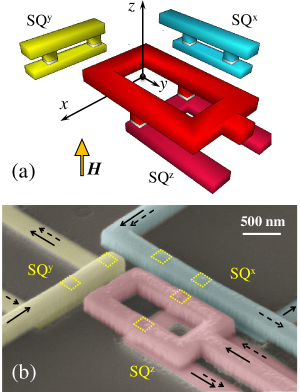
A scheme of the three-axis nanoSQUID is shown in Fig. 1(a). Two perpendicular stripline nanoloops, SQx and SQy, are devoted to measure the and components of , respectively. The component of the magnetic moment is sensed by a third planar first-order gradiometer, SQz, designed to be insensitive to uniform magnetic fields applied along but sensitive to the imbalance produced by a small magnetic signal in one of the two SQUID loops. Strictly speaking, the device reveals the three components of if and only if the magnetic moment is placed at the intersection between the three nanoloop axes. In practice, this position approaches as indicated by a black dot in Fig. 1(a). We note that corresponds to the interface of the upper Nb layer and the SiO2 layer, which separates top and bottom Nb. Later on we will demonstrate that this constraint is actually flexible enough to realize three-axis magnetic detection of MNPs with finite volume, even if these are not positioned with extreme accuracy.
Figure 1(b) shows a false colored scanning electron microscopy (SEM) image of a typical device. The junction barriers are made of normal metallic HfTi layers with thickness nm. The bottom and top Nb layer are, respectively, and nm-thick and are separated by a nm-thick SiO2 layer. Nb wirings are nm wide and the Josephson junctions are square-shaped with area . The inner loop area of SQx and SQy corresponds to whereas SQz consist of two parallel-connected loops with inner area of . This configuration allows the application of moderate homogeneous magnetic fields along that do not couple any flux neither to the nanoloops of SQx and SQy nor to the junctions in the -plane of all three nanoSQUIDs.
The bias currents and modulation currents flow as indicated in Fig. 1(b) by black solid and dashed arrows, respectively. The latter are used to couple flux to each nanoSQUID individually, so to linearize their flux-to-voltage transfer function in FLL operation.
II.2 Electric transport and noise data
The Nb/HfTi/Nb junctions have typical critical current densities at K and resistance times junction area . As a result, large characteristic voltages up to V can be obtained. These junctions are intrinsically shunted providing, therefore, non-hysteretic current-voltage characteristics.Wölbing et al. (2013); Nagel et al. (2011a)
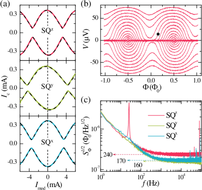
Electric transport data of a typical device are shown in Fig. 2. From the period of the maximum critical current shown in panel (a) we can deduce the mutual inductance between SQi and its corresponding modulation line (). Asymmetries observed in these data for positive and negative bias current arise from the asymmetric distribution of [see black solid arrows in Fig. 1(b)]. The strongest asymmetry is found for SQy, which is attributed to the sharp corner in the bottom Nb strip right below one of the two Josephson junctions (see Fig. 1, upper right junction of SQy). Numerically calculated curves based on the resistively and capacitively shunted junction (RCSJ)-model, including thermal noise, are fitted to these experimental data in order to estimate and [black dashed lines in Fig. 2(a)]. Here, is the average critical current of the two junctions intersecting the nanoloop, and is its inductance. Asymmetric biasing is included in the model through an inductance asymmetry where and are the inductances of the two SQUID arms. On the other hand, the maximum transfer coefficient can be experimentally determined by coupling via and measuring the resulting for different as shown in Fig. 2(b). Following this approach, we have characterized a number of devices obtaining very low dispersion. Few examples are provided in Table 1, which gives evidence of the high quality and reproducibility of the fabrication process.
Finally, cross-talking between the three nanoSQUIDs can be quantified by the mutual inductances (), i.e., the flux coupled to SQi by the modulation current in SQj. If the three orthogonal SQUIDs are operated in FLL, a signal detected by SQj will be compensated by the feedback current . This will also couple the (cross-talk) flux to SQi. As is typically two orders of magnitude below , this effect is negligible in most cases (see Methods section). Moreover, it can be avoided by operating the devices in open-loop readout.
The operation of the sensor upon externally applied magnetic fields was investigated as well. For this purpose, the output voltage response of all three nanoSQUIDs operating in FLL-mode was recorded upon sweeping for a number of devices. Under optimum conditions, a negligible flux is coupled to SQx and SQy whereas, due to imperfect balancing, SQz couples mT. This imbalance results mainly from the asymmetric Nb wiring surrounding SQz and the intrinsic errors associated to the fabrication. All sensors are fully operative up to mT, where abrupt changes in the response of the device are observed. This behavior is attributed to the entrance of Abrikosov vortices in the Nb wires close to the nanoSQUIDs as it has been observed in similar devices.Nagel et al. (2013); Wölbing et al. (2013)
| (mA) | (A) | (V) | (pH) | (V/) | ||||
|---|---|---|---|---|---|---|---|---|
| A2 | SQx | 7.0 | 187 | 67 | 0.20 | 1.0 | 0 | 340 |
| SQy | 8.8 | 176 | 62 | 0.14 | 0.8 | 0.60 | 390 | |
| SQz | 6.5 | 183 | 66 | 0.22 | 1.2 | 0.25 | 330 | |
| D5 | SQx | 7.7 | 136 | 57 | 0.14 | 1.1 | 0 | 250 |
| SQy | 9.0 | 136 | 59 | 0.12 | 0.9 | 0.75 | 260 | |
| SQz | 5.7 | 145 | 58 | 0.16 | 1.1 | 0.35 | 240 | |
| C3 | SQx | 8.0 | 120 | 55 | 0.20 | 1.7 | 0 | 120 |
| SQy | 9.1 | 128 | 54 | 0.32 | 2.6 | 0.40 | 110 | |
| SQz | 5.8 | 134 | 57 | 0.18 | 1.4 | 0.28 | 170 |
Fig. 2(c) shows the spectral density of rms flux noise obtained with each nanoSQUID operating in FLL mode after low-temperature amplification using a commercial SQUID series array amplifier (SSA). The peak observed at Hz for SQz is attributed to mechanical vibrations. Ubiquitous -noise dominates for Hz in all three spectra. Remarkably low values are obtained in the white region, yielding , 160 and 240 n for SQx, SQy and SQz, respectively.
The flux noise can be translated into the spin sensitivity , which is the figure of merit of nanoSQUID sensors. Here, the coupling factor is the magnetic flux per magnetic moment , which is coupled to the SQUID from a MNP with magnetic moment placed at position . The coupling factor can be calculated as , where is the normalized magnetic field created at position by a supercurrent circulating in the nanoloop.Wölbing et al. (2014); Nagel et al. (2011b) We note that depends on both the particle position (relative to the nanoloop) and the orientation of its magnetic moment. We simulate by solving the London equations for the specific geometry of each nanoSQUID (see Methods section). For a particle at position [see Fig. 1(a)] we obtain for SQi spin sensitivities , 650 and for , respectively. The spin sensitivity for SQz is much better than for SQx and SQy, because is much closer to SQz than to SQx and SQy.
II.3 Analysis of vector magnetometer performance
In the following we analyze the capability of this device to distinguish between the three components of . For this purpose we write the normalized field created by each SQUID SQi as , i.e., we split this into a component along the direction and a component perpendicular to that, with (). Ideally, for each of the three SQUIDs SQi, , i.e., . In that case, each SQUID SQi is sensitive to the component only, and one can reconstruct the magnitude and orientation from the signals detected by the three orthogonal SQUIDs.
To quantify the deviation from that ideal case, we define the relative error flux made by nanoSQUID SQi. Here, relates to the ideal case in which the moment is oriented along . In contrast, corresponds to the worst case when the moment is oriented along , which yields the maximum error. Hence, the relative error flux is given by
This definition assures that does not depend on the orientation of the magnetic moment of the particle, but only on its position .
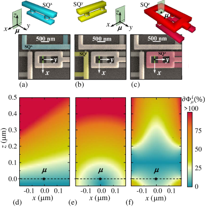
The relative error flux for our device is first calculated at giving and . Much better results can be obtained for SQx and SQy at m giving and . We note that this region becomes accessible after drilling a hole in the SiO2 layer which is feasible by means of, e.g., focused ion beam milling.
We determine now deviations on the particle position that still lead to a tolerable level of error. For this purpose is calculated in the --plane (at =0) as indicated in Fig. 3(a), (b) and (c). The results obtained for SQx, SQy and SQz are shown in (d), (e) and (f), respectively. The white line in these color plots corresponds to . As it can be seen, SQy imposes more severe restrictions on the particle position. More specifically, is obtained at and nm, whereas results at nm. Due to the symmetry of the problem the behavior of SQx and SQy is interchanged if one considers the --plane.
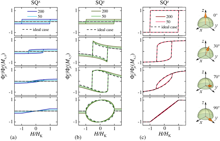
We finish by showing how this device can indeed serve to provide full insight on the three-dimensional properties of MNPs of finite size and the mechanisms that lead to the magnetization reversal. It will be instructive to start this discussion by focusing on the flux coupled by a point-like MNP to an ideal three-axis magnetometer, i.e., we assume for . We consider for simplicity that the particle exhibits uniaxial anisotropy along a given direction , so that magnetic states pointing along are separated by an energy barrier. In that case, the particle will exhibit a typical hysteretic behavior when sweeping the external magnetic field . This behavior will lead, however, to very different signals seen by each nanoSQUID, and those signals can strongly depend on the orientation of the easy axis with respect to the applied field direction. This is represented in Fig. 4, where the flux coupled to SQi is plotted vs. for (a), (b), (c) (dashed black lines). The different panels correspond to different orientation of the easy axis, from (top) to (bottom), as sketched on the right side of Fig. 4.
Let us first consider the case in which the easy axis points along the externally applied magnetic field, i.e., . As it can be seen, no flux is coupled to SQx and SQy as lies always parallel to whereas SQz senses the maximum amount of flux possible. In the latter case, abrupt steps correspond to the switching of between the states which leads to a typical squared-shaped hysteresis curve. The situation changes dramatically if one assumes that the easy axis points perpendicular to . Under these circumstances, the particle’s magnetic moment tilts progressively as the external magnetic field is swept so that no abrupt steps are observed in the hysteresis curves. This is exemplified in the bottom panels of Fig. 4 which result when . As it can be seen, remains zero during the whole sweep whereas is obtained only when the particle is saturated along leading to the maximum flux coupled by SQz. Remarkably, reaches a maximum (minimum) at when () whereas accounts for the progressive tilting of as is swept. Intermediate situations result when the easy axis points along different directions in space as it is exemplified in the middle panels.
Interestingly, a very similar behavior is observed when simulating a real experiment in which an extended MNP is measured using the three-axis nanoSQUID described here. To illustrate this we have computed numerically when semi-spheres with radius and 200 nm centered at position are considered (see Methods section). As it can be seen in Fig. 4 (solid lines) finite and the particle’s volume does not affect noticeably the flux coupled to SQz, whereas it slightly changes the flux coupled to SQx and SQy. This behavior can be easily understood, as the spatial extension of relatively large particles still remains in the region confined below the white line in Fig. 3(f), whereas they occupy zones with larger and in panels (d) and (e). Still, our simulations demonstrate the operation of the device as a three-axis vector magnetometer even if relatively large MNPs are investigated. The inspection of the hysteresis curves recorded simultaneously with all three nanoSQUIDs, together with the knowledge of the particle volume, allow extracting full information on the particle’s anisotropy in a real experiment.
II.4 Conclusions
We have successfully fabricated three close-lying orthogonal nanoSQUIDs leading to the nanoscopic version of a three-axis vector magnetometer. All three nanoSQUIDs can be operated simultaneously in open- or flux-locked loop mode to sense the stray magnetic field produced by an individual MNP located at position . The device operates at K and is insensitive to the application of external magnetic fields perpendicular to the substrate plane (along ) up to mT. The latter can be used to induce the magnetization reversal of the MNP under study. The limiting operation field can be increased in the future by improving the design. This implies reducing the linewidths so to increase the critical field for vortex entry and improving the balancing of the gradiometric nanoSQUID.
We have demonstrated the ability of this device to distinguish between the three orthogonal components of the vector magnetic moment by calculating the spatial dependence of the total relative error flux. The latter yields values below for particles located at nm. For we obtain a total spin sensitivity , 650 and for the , and components of , respectively. Finally, a model case has been described in which the three-axis vector nanoSQUID can be used to obtain full insight into the three-dimensional anisotropy of an extended MNP with diameter nm. For this purpose, the signal captured by each nanoSQUID is used to reconstruct the magnitude and orientation of the magnetic moment during the magnetization reversal.
III Methods
III.1 Sample Fabrication
The fabrication combines electron-beam lithography (EBL) and chemical-mechanical polishing (CMP).Hagedorn et al. (2006) A Si wafer with a nm-thick thermally oxidized layer is used as a substrate. An Al2O3 etch stop layer is first deposited by RF sputtering. Then, the SNS tri-layer consisting of Nb/Hf50wt%Ti50wt%/Nb is sputtered in-situ. The next step serves to define the SNS Josephson junctions by means of an Al etching mask defined by EBL and lift-off. The pattern is transferred to the Nb/HfTi/Nb tri-layer through reactive ion etching (RIE) in a SF6 plasma and Ar ion beam acting on the counter Nb and HfTi layers, respectively. The bottom Nb layer is directly patterned using a negative EBL resist mask and SF6-based RIE. In the following step, a 600 nm-thick layer of insulating SiO2 is deposited through plasma enhanced chemical vapor deposition and subsequently polished through CMP. This process guarantees good wafer smoothing and electric contact to the Nb counter electrodes. In the last step, the wiring Nb layer is sputtered and patterned using an EBL Al etching mask and SF6-based RIE.
III.2 Measurement of electric transport properties and noise
Current bias is performed by means of battery powered low-noise current sources and the output voltage is amplified at room temperature. Each single nanoSQUID can be operated in flux-locked loop mode simultaneously, by using commercial three-channel SQUID readout electronics. Additionally, the output signal can be amplified at low temperatures using commercial SQUID series arrays amplifiers. High-field measurements are performed in a cryostat hosting a vector magnet, whereas noise measurements are performed in a magnetically and high-frequency shielded environment. All measurements described here were performed with the devices immersed in liquid 4He, at K.
III.3 Numerical simulations
Fitting of the experimental data is based on the RCSJ model.Chesca et al. (2004) The response of the SQUID is described by two coupled Langevin equations, and . Here, is the phase difference for the two junctions () and and are, respectively, the bias and circulating currents normalized to . Nyquist noise is included through two independent normalized current noise sources . Additionally, , where is the external flux normalized to . Finally, , , , and and are the resistance and capacitance of the SQUID, respectively. In the model, the total inductance of the loop accounts for both the geometrical and the kinetic contributions. The total dc voltage across the SQUID is calculated as the time average , where . We emphasize here that the magnitude of does not affect the modulation of and, therefore, our estimation of and . In all fittings has been assumed for convenience, as in Chesca et al. Chesca et al. (2004).
| nm | nm | |||||||||||
| (A) | (A) | (m) | (m) | (m) | (m) | |||||||
| SQx | 132 | – | 0.49 | 1.2 | 10 | – | 0.044 | 1.4 | 600 | – | 2.6 | 72 |
| SQy | 112 | 1.5 | – | 0.82 | 10 | 0.11 | – | 0.98 | 600 | 6.8 | – | 49 |
| SQz | 167 | 1.4 | 6.1 | – | 200 | 0.11 | 0.55 | – | 6.4 | 33 | – | |
For the estimation of the spin sensitivity and the relative error flux one needs to calculate the spatial distribution of created by each SQi. For this purpose we have used the numerical simulation software 3D-MLSIKhapaev et al. (2003) which is based on a finite element method to solve the London equations in a superconductor with a given geometry, film thickness and London penetration depth ( nm). and with being the supercurrent in the nanoloop. For SQz one needs to consider two circular currents flowing around each nanoloop. The resulting normalized magnetic field is, in this case, .
For the simulation of the hysteresis curves we consider first an ideal point-like MNP with magnetic moment described by the polar coordinates and characterized by one second-order anisotropy term. If both and the easy axis lie in the --plane the problem is reduced to the minimization of in two dimensions (). Here is the total energy normalized to the anisotropy barrier height, is the field normalized to the anisotropy field, is the angle between and the easy axis and is the angle between and the easy axis. Solutions of for , , and yield the values of
plotted in Fig. 4. Notice that, in this case, so that leading to , and .
For the simulation of extended particles we assume that all magnetic moments lie parallel to each other during the magnetization reversal. In this way, the exchange energy can be neglected and the expression for given above is still valid (Stoner-Wohlfarth model). Here, the second-order anisotropy term might also account for the shape anisotropy introduced by the magnetostatic energy. In this case one needs to integrate over the volume () of the whole MNP leading to
Assuming, e.g., a semisphere made of hcp cobalt ( /atom and density g/cm3) one obtains m and m for nm and and for nm. For these specific examples, we can compare the flux signals quoted above with the corresponding cross-talk signals appearing in FLL operation. For the calculation of , we used the experimentally determined values for of device D5 and the average values obtained from the measured values of all three devices A2, D5 and C3 (from Table 1). These values are listed in Table 2 together with and . We find that the cross-talk in FLL operation is on the percent level or even below, except for and , where it is around 10 %.
Acknowledgements.
M. J. M.-P. acknowledges support by the Alexander von Humboldt Foundation, D. G. acknowledges support by the EU-FP6-COST Action MP1201. This work is supported by the Nachwuchswissenschaftlerprogramm of the Universität Tübingen, by the Deutsche Forschungsgemeinschaft (DFG) via Projects KO 1303/13-1, KI 698/3-1, and SFB/TRR 21 C2 and by the EU-FP6-COST Action MP1201.References
- Martínez-Pérez et al. (2010) M. J. Martínez-Pérez, R. de Miguel, C. Carbonera, M. Martínez-Júlvez, A. Lostao, C. Piquer, C. Gómez-Moreno, J. Bartolomé, and F. Luis, “Size-dependent properties of magnetoferritin.” Nanotechnology 21, 465707 (2010).
- Silva et al. (2005) N. J. O. Silva, V. S. Amaral, and L. D. Carlos, “Relevance of magnetic moment distribution and scaling law methods to study the magnetic behavior of antiferromagnetic nanoparticles: Application to ferritin.” Phys. Rev. B 71, 184408 (2005).
- Granata and Vettoliere (2016) C. Granata and A. Vettoliere, “Nano superconducting quantum interference device: A powerful tool for nanoscale investigations.” Phys. Rep. 614, 1 – 69 (2016).
- Schwarz et al. (2015) T. Schwarz, R. Wölbing, C. F. Reiche, B. Müller, M. J. Martínez-Pérez, T. Mühl, B. Büchner, R. Kleiner, and D. Koelle, “Low-noise YBa2Cu3O7 nano-SQUIDs for performing magnetization-reversal measurements on magnetic nanoparticles.” Phys. Rev. Appl. 3, 044011 (2015).
- Buchter et al. (2015) A. Buchter, R. Wölbing, M. Wyss, O. F. Kieler, T. Weimann, J. Kohlmann, A. B. Zorin, D. Rüffer, F. Matteini, G. Tütüncüoglu, F. Heimbach, A. Kleibert, A. Fontcuberta i Morral, D. Grundler, R. Kleiner, D. Koelle, and M. Poggio, “Magnetization reversal of an individual exchange-biased permalloy nanotube.” Phys. Rev. B 92, 214432 (2015).
- Shibata et al. (2015) Y. Shibata, S. Nomura, H. Kashiwaya, S. Kashiwaya, R. Ishiguro, and H. Takayanagi, “Imaging of current density distributions with a nb weak-link scanning nano-squid microscope.” Sci. Rep. 5, 15097 (2015).
- Schmelz et al. (2015) M. Schmelz, Y. Matsui, R. Stolz, V. Zakosarenko, T. Schönau, S. Anders, S. Linzen, H. Itozaki, and H.-G. Meyer, “Investigation of all niobium nano-SQUIDs based on sub-micrometer cross-type Josephson junctions,” Supercond. Sci. Technol. 28, 015004 (2015).
- Vasyukov et al. (2013) D. Vasyukov, Y. Anahory, L. Embon, D. Halbertal, J. Cuppens, L. Neeman, A. Finkler, Y. Segev, Y. Myasoedov, M. L. Rappaport, M. E. Huber, and E. Zeldov, “A scanning superconducting quantum interference device with single electron spin sensitivity.” Nat. Nanotechnol. 8, 639 (2013).
- Arpaia et al. (2014) R. Arpaia, M. Arzeo, S. Nawaz, S. Charpentier, F. Lombardi, and T. Bauch, “Ultra low noise YBa2Cu3O7-δ nano superconducting quantum interference devices implementing nanowires,” App. Phys. Lett. 104, 072603 (2014).
- Hazra et al. (2014) D. Hazra, J. R. Kirtley, and K. Hasselbach, “Nano-superconducting quantum interference devices with suspended junctions,” Appl. Phys. Lett. 104, 152603 (2014).
- Wölbing et al. (2013) R. Wölbing, J. Nagel, T. Schwarz, O. Kieler, T. Weimann, J. Kohlmann, A. B. Zorin, M. Kemmler, R. Kleiner, and D. Koelle, “Nb nano superconducting quantum interference devices with high spin sensitivity for operation in magnetic fields up to 0.5 T.” Appl. Phys. Lett. 102, 192601 (2013).
- Levenson-Falk et al. (2013) E. M. Levenson-Falk, R. Vijay, N. Antler, and I. Siddiqi, “A dispersive NanoSQUID magnetometer for ultra-low noise, high bandwidth flux detection,” Supercond. Sci. Technol. 26, 055015 (2013).
- Buchter et al. (2013) A. Buchter, J. Nagel, D. Rüffer, F. Xue, D. P. Weber, O. F. Kieler, T. Weimann, J. Kohlmann, A. B. Zorin, E. Russo-Averchi, R. Huber, P. Berberich, A. Fontcuberta i Morral, M. Kemmler, R. Kleiner, D. Koelle, D. Grundler, and M. Poggio, “Reversal mechanism of an individual Ni nanotube simultaneously studied by torque and SQUID magnetometry.” Phys. Rev. Lett. 111, 067202 (2013).
- Bellido et al. (2013) E. Bellido, P. González-Monje, A. Repollés, M. Jenkins, J. Sesé, D. Drung, T. Schurig, K. Awaga, F. Luis, and D. Ruiz-Molina, “Mn12 single molecule magnets deposited on -SQUID sensors: the role of interphases and structural modifications.” Nanoscale 5, 12565–12573 (2013).
- Granata et al. (2013) C. Granata, A. Vettoliere, R. Russo, M. Fretto, N. De Leo, and V. Lacquaniti, “Three-dimensional spin nanosensor based on reliable tunnel josephson nano-junctions for nanomagnetism investigations.” Appl. Phys. Lett. 103, 102602 (2013).
- Martínez-Pérez et al. (2011) M. J. Martínez-Pérez, E. Bellido, R. de Miguel, J. Sesé, A. Lostao, C. Gómez-Moreno, D. Drung, T. Schurig, D. Ruiz-Molina, and F. Luis, “Alternating current magnetic susceptibility of a molecular magnet submonolayer directly patterned onto a micro superconducting quantum interference device.” Appl. Phys. Lett. 99, 032504 (2011).
- Hao et al. (2011) L. Hao, C. Aßmann, J. C. Gallop, D. Cox, F. Ruede, O. Kazakova, P. Josephs-Franks, D. Drung, and Th. Schurig, “Detection of single magnetic nanobead with a nano-superconducting quantum interference device.” Appl. Phys. Lett. 98, 092504 (2011).
- Kirtley (2010) J. R. Kirtley, “Fundamental studies of superconductors using scanning magnetic imaging,” Rep. Prog. Phys. 73, 126501 (2010).
- Giazotto et al. (2010) Francesco Giazotto, Joonas T. Peltonen, Matthias Meschke, and Jukka P. Pekola, “Superconducting quantum interference proximity transistor,” Nature Phys. 6, 254–259 (2010).
- Vohralik and Lam (2009) P. F. Vohralik and S. K. H. Lam, “Nanosquid detection of magnetization from ferritin nanoparticles.” Supercond. Sci. Technol. 22, 064007 (2009).
- Huber et al. (2008) Martin E. Huber, Nicholas C. Koshnick, Hendrik Bluhm, Leonard J. Archuleta, Tommy Azua, Per G. Björnsson, Brian W. Gardner, Sean T. Halloran, Erik A. Lucero, and Kathryn A. Moler, “Gradiometric micro-squid susceptometer for scanning measurements of mesoscopic samples,” Rev. Sci. Instrum. 79, 053704 (2008).
- Hao et al. (2008) L. Hao, J. C. Macfarlane, J. C. Gallop, D. Cox, J. Beyer, D. Drung, and T. Schurig, “Measurement and noise performance of nano-superconducting-quantum-interference devices fabricated by focused ion beam,” Appl. Phys. Lett. 92, 192507 (2008).
- Wernsdorfer (2001) W. Wernsdorfer, “Classical and quantum magnetization reversal studied in nanometersized particles and clusters,” Adv. Chem. Phys. 118, 99–190 (2001), arXiv:cond-mat/0101104v1 .
- Jamet et al. (2001) M. Jamet, W. Wernsdorfer, C. Thirion, D. Mailly, V. Dupuis, P. Mélinon, and A. Pérez, “Magnetic anisotropy of a single cobalt nanocluster,” Phys. Rev. Lett. 86, 4676–4679 (2001).
- Wernsdorfer et al. (1995) W. Wernsdorfer, K. Hasselbach, D. Mailly, B. Barbara, A. Benoit, L. Thomas, and G. Suran, “Dc-SQUID magnetization measurements of single magnetic particles.” J. Magn. Magn. Mat. 145, 33–39 (1995).
- Awschalom et al. (1992) D. D. Awschalom, J. F. Smyth, G. Grinstein, D. P. DiVincenzo, and D. Loss, “Macroscopic quantum tunneling in magnetic proteins.” Phys. Rev. Lett. 68, 3092–3095 (1992).
- Lipert et al. (2010) K. Lipert, S. Bahr, F. Wolny, P. Atkinson, U. Weißker, T. Mühl, O. G. Schmidt, B. Büchner, and R. Klingeler, “An individual iron nanowire-filled carbon nanotube probed by micro-Hall magnetometry.” Appl. Phys. Lett. 97, 212503 (2010).
- Kent et al. (1994) A. D. Kent, S. von Molnár, S. Gider, and D. D. Awschalom, “Properties and measurement of scanning tunneling microscope fabricated ferromagnetic particle arrays.” J. Appl. Phys. 76, 6656–6660 (1994).
- Thiel et al. (2016) L. Thiel, D. Rohner, M. Ganzhorn, P. Appel, E. Neu, B. Müller, R. Kleiner, D. Koelle, and P. Maletinsky, “Quantitative nanoscale vortex imaging using a cryogenic quantum magnetometer,” Nat. Nanotechnol. (2016), 10.1038/nnano.2016.63, dOI: 10.1038/nnano.2016.63.
- Schäfer-Nolte et al. (2014) E. Schäfer-Nolte, L. Schlipf, M. Ternes, F. Reinhard, K. Kern, and J. Wrachtrup, “Tracking temperature-dependent relaxation times of ferritin nanomagnets with a wideband quantum spectrometer,” Phys. Rev. Lett. 113, 217204 (2014).
- Rondin et al. (2013) L. Rondin, J. P. Tetienne, S. Rohart, A. Thiaville, T. Hingant, P. Spinicelli, J. F. Roch, and V. Jacques, “Stray-field imaging of magnetic vortices with a single diamond spin.” Nat. Commun. 4, 2279 (2013).
- Nagel et al. (2013) J. Nagel, A. Buchter, F. Xue, O. F. Kieler, T. Weimann, J. Kohlmann, A. B. Zorin, D. Rüffer, E. Russo-Averchi, R. Huber, P. Berberich, A. Fontcuberta i Morral, D. Grundler, R. Kleiner, D. Koelle, M. Poggio, and M. Kemmler, “Nanoscale multifunctional sensor formed by a Ni nanotube and a scanning Nb nanoSQUID.” Phys. Rev. B 88, 064425 (2013).
- Rugar et al. (2004) D. Rugar, R. Budakian, H. J. Mamin, and B. W. Chui, “Single spin detection by magnetic resonance force microscopy.” Nature 430, 329–332 (2004).
- Shinjo et al. (2000) T. Shinjo, T. Okuno, R. Hassdorf, K. Shigeto, and T. Ono, “Magnetic vortex core observation in circular dots of permalloy.” Science 289, 930–932 (2000).
- Ganzhorn et al. (2013) M. Ganzhorn, S. Klyatskaya, M. Ruben, and W. Wernsdorfer, “Carbon nanotube nanoelectromechanical systems as magnetometers for single-molecule magnets,” ACS Nano 7, 6225–6236 (2013).
- Stipe et al. (2001) B. C. Stipe, H. J. Mamin, T. D. Stowe, T. W. Kenny, and D. Rugar, “Magnetic dissipation and fluctuations in individual nanomagnets measured by ultrasensitive cantilever magnetometry,” Phys. Rev. Lett. 86, 2874–2877 (2001).
- Thiaville (2000) A. Thiaville, “Coherent rotation of magnetization in three dimensions: A geometrical approach.” Phys. Rev. B 61, 12221–12232 (2000).
- Stoner and Wohlfarth (1948) E. C. Stoner and E. P. Wohlfarth, “A mechanism of magnetic hysteresis in heterogeneous alloys,” Philos. Trans. R. Soc. London, Ser. A 240, 599–642 (1948).
- Aharoni (1966) A. Aharoni, “Magnetization curling,” Phys. Status Solidi B 16, 3–42 (1966).
- Schott et al. (2000) Ch. Schott, J.-M. Waser, and R. S. Popovic, “Single-chip 3-D silicon Hall sensor.” Sens. Actuators 82, 167–173 (2000).
- Miyajima et al. (2015) S. Miyajima, T. Okamoto, H. Matsumoto, H.T. Huy, M. Hayashi, M. Maezawa, M. Hidaka, and T. Ishida, “Vector pickup system customized for scanning SQUID microscopy.” IEEE Trans. Appl. Supercond. 25, 1600704 (2015).
- Ketchen et al. (1997) M.B. Ketchen, J.R. Kirtley, and M. Bhushan, “Miniature vector magnetometer for scanning SQUID microscopy.” IEEE Trans. Appl. Supercond. 7, 3139–3142 (1997).
- Anahory et al. (2014) Y. Anahory, J. Reiner, L. Embon, D. Halbertal, A. Yakovenko, Y. Myasoedov, M. L. Rappaport, M. E. Huber, and E. Zeldov, “Three-junction SQUID-on-tip with tunable in-plane and out-of-plane magnetic field sensitivity,” Nano Lett. 14, 6481–6487 (2014).
- Hagedorn et al. (2006) D. Hagedorn, O. Kieler, R. Dolata, R. Behr, F. Müller, J. Kohlmann, and J. Niemeyer, “Modified fabrication of planar sub-m superconductor-normal metal-superconductor Josephson junctions for use in a Josephson arbitrary waveform synthesizer,” Supercond. Sci. Technol. 19, 294–298 (2006).
- Nagel et al. (2011a) J. Nagel, O. F. Kieler, T. Weimann, R. Wölbing, J. Kohlmann, A. B. Zorin, R. Kleiner, D. Koelle, and M. Kemmler, “Superconducting quantum interference devices with submicron Nb/HfTi/Nb junctions for investigation of small magnetic particles.” Appl. Phys. Lett. 99, 032506 (2011a).
- Drung (2003) D. Drung, “High- and low- dc SQUID electronics,” Supercond. Sci. Technol. 16, 1320–1336 (2003).
- Wölbing et al. (2014) R. Wölbing, T. Schwarz, B. Müller, J. Nagel, M. Kemmler, R. Kleiner, and D. Koelle, “Optimizing the spin sensitivity of grain boundary junction NanoSQUIDs – towards detection of small spin systems with single-spin resolution.” Supercond. Sci. Technol. 27, 125007 (2014).
- Nagel et al. (2011b) J. Nagel, K. B. Konovalenko, M. Kemmler, M. Turad, R. Werner, E. Kleisz, S. Menzel, R. Klingeler, B. Büchner, R. Kleiner, and D. Koelle, “Resistively shunted YBa2Cu3O7 grain boundary junctions and low-noise SQUIDs patterned by a focused ion beam down to 80 nm linewidth.” Supercond. Sci. Technol. 24, 015015 (2011b).
- Chesca et al. (2004) B. Chesca, R. Kleiner, and D. Koelle, in The SQUID Handbook, Vol. 1, edited by John Clarke and Alex I. Braginski (Wiley-VCH, Weinheim, 2004) Chap. 2, pp. 29–92.
- Khapaev et al. (2003) M. M. Khapaev, M. Yu Kupriyanov, E. Goldobin, and M. Siegel, “Current distribution simulation for superconducting multi-layered structures.” Supercond. Sci. Technol. 16, 24 (2003).