Study on the high spectral intensity at the Dirac energy of single-layer graphene on an SiC substrate
Abstract
We have investigated electron band structure of epitaxially grown graphene on an SiC(0001) substrate using angle-resolved photoemission spectroscopy. In single-layer graphene, abnormal high spectral intensity is observed at the Dirac energy whose origin has been questioned between in-gap states induced by the buffer layer and plasmaron bands induced by electron-plasmon interactions. With the formation of double-layer graphene, the Dirac energy does not show the high spectral intensity any longer different from the single-layer case. The inconsistency between the two systems suggests that the main ingredient of the high spectral intensity at the Dirac energy of single-layer graphene is the electronic states originating from the coupling of the graphene bands to the localized states of the buffer layer, consistent with the theoretical prediction on the presence of in-gap states.
I Introduction
The charge neutral point , where conduction and valence bands touch at a single point, reveals an important aspect of the physics of graphene Neto . For example, when is aligned to Fermi energy , graphene shows strong electronic correlations that are not explained by the theory that describes typical metallic systems HwangSR . Upon introducing dopants (or charges), many-body effects are developed to show well-defined quasiparticle states near induced by electron-plasmon interactions, so-called plasmaron bands, right next to the well-known graphene bands MacDonald1 ; MacDonald2 ; Eli1 ; Eli2 . Such electronic correlations are strongly affected by the presence of a substrate. Especially, when dielectric screening from the substrate becomes stronger compared to that for free-standing graphene, the plasmaron bands approach towards the graphene bands, so that they are not resolved, but leave their signature as high spectral intensity at Eli1 ; Eli2 .
Alternatively the electron band structure itself can result in the spectral feature at . On the surface of an SiC(0001) substrate, a carbidic layer, so-called buffer layer, is formed with the same geometric structure as graphene in the absence of the characteristic conical dispersion due to the formation of covalent bonds with the substate Varchon . Upon the formation of single-layer graphene on top of it, the presence of the buffer layer breaks the sublattice symmetry of the single-layer graphene resulting in an energy gap at Kim ; Lee ; Zhou07 ; Rusponi . Meanwhile localized states of the buffer layer couple to the graphene bands which contributes to finite spectral intensity at , i. e. , in-gap states, despite the plasmaron bands are not taken into account Kim . In fact, recent GW calculations give no well-defined plasmaron bands in the epitaxial doped single-layer graphene on an SiC substrate Louie , in contrast to the previous theoretical MacDonald1 ; MacDonald2 and experimental results Eli1 ; Eli2 .
Here we investigate this controversial issue by comparing the electron band structure of single- and double-layer graphene samples using angle-resolved photoemission spectroscopy (ARPES). Single-layer graphene shows high spectral intensity at consistent with previous results Eli2 ; Zhou07 . On the other hand, in double-layer graphene, we observe that the electron band structure shows a dip in spectral intensity at . The difference in the spectral feature is well described in terms of the in-gap states, whereas the plasmaron bands does not explain the weak spectral intensity observed at of double-layer graphene on an SiC(0001) substrate and even single-layer graphene on metallic substrates. Our results suggest that the in-gap states induced by the buffer layer Kim are the main ingredient of the controversial high spectral intensity at of single-layer graphene on the SiC substrate.
II Experimental methods
Graphene samples were prepared by the epitaxial growth method on an SiC(0001) substrate Rolling and the chemical vapour deposition method on a Cu film Hong . High-resolution ARPES experiments have been performed on the graphene samples using a synchrotron source with an energy of 50 eV at beamline 12.0.1 of the Advanced Light Source at Lawrence Berkeley National Laboratory. The energy and angular resolutions are 32 meV and 0.3∘, respectively. All the measurements have been performed at 15 K in ultra-high vacuum with a base pressure of 3.510-11 Torr.
III Results and Discussions
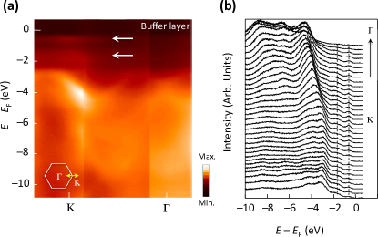
Figure 1(a) shows an ARPES intensity map of a buffer layer sample taken along the direction of the graphene unit cell denoted in the inset, which is consistent with the previous results Emtsev . More specifically, near two non-dispersive states are observed at 1.7 eV and 0.5 eV below as denoted by white arrows. Such a non-dispersive feature is also clear in energy distribution curves (EDCs) taken at different momentum values as denoted by dashed lines in Fig. 1(b). The former originates from the Si dangling bond states which belong to the Si-rich surface of the SiC(0001) substrate, so-called phase, formed before the buffer layer is grown on the substrate Emtsev . With the formation of the buffer layer, several flat bands are predicted below originating from the -orbitals of carbon atoms Kim , which are observed as the non-dispersive state 0.5 eV below . The observation of the two non-dispersive states suggests that the sample is not fully covered by the buffer layer, but consists of both buffer layer and the phase.
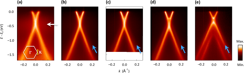
To investigate the latter non-dispersive state, we have measured ARPES intensity maps of several different graphene samples taken perpendicular to the direction of graphene unit cell as denoted by the yellow arrow in the inset. Figure 2(a) shows the bands of single-layer graphene that are intrinsically doped by electrons due to the presence of the SiC substrate Seyller , so that lies 0.43 eV below . The measured ARPES intensity map exhibits two additional features in addition to the characteristic conical dispersion: (i) finite spectral intensity away from the graphene bands as denoted by the white arrow; (ii) strong spectral intensity at in the graphene bands. The former is the non-dispersive state observed from the buffer layer in Fig. 1. Coexistence of the non-dispersive state and the graphene bands suggests that the sample consists of single-layer graphene as well as the buffer layer, consistent with previous microscopy results Siegel . The origin of the latter has been argued between the in-gap states Kim and the plasmaron bands Eli1 . As we go from the sample shown in Fig. 2(a) to Fig. 2(d), spectral weight of another band structure develops as denoted by the blue arrows, until it becomes very clear in Fig. 2(e) to show the characteristic electron band structure of double-layer graphene.
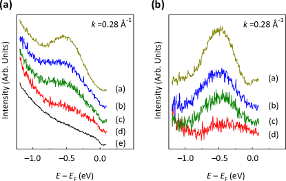
It is interesting to note that the finite spectral intensity denoted by the white arrow in Fig. 2(a) becomes weaker as we go towards the double-layer graphene sample shown in Fig. 2(e), which is obvious when we take EDCs at for each sample. Figure 3(a) shows normalized EDCs, when (a)-(e) denote that each spectrum is taken from Fig. 2(a)-(e), respectively. Figure 3(b) shows the normalized EDCs after subtracting spectral intensity of double-layer graphene denoted by (e) in Fig. 2(a). The intensity of the well-defined peak shape at decreases as we go from the sample shown in Fig. 2(a) to Fig. 2(d), which becomes featureless for the double-layer graphene sample (e). It is known that, as the graphene layers develop, the buffer layer is increasingly covered by the graphene overlayers Siegel . The previous first principles calculations show that the localized states of the buffer layer couple to the graphene bands giving rise to finite spectral intensity at of single-layer graphene on an SiC(0001) substrate. Within this theory, upon the evolution of graphene overlayers, the buffer layer states are increasingly coupled to the graphene bands, resulting in gradual decrease of spectral intensity of the buffer layer states. This is consistent with what we have observed in Figs. 2 and 3.
Alternatively, due to the finite mean free path of electrons within a solid, increasing thickness of graphene layers can reduce photoelectron intensity from the buffer layer states. Indeed, as we go from Fig. 2(a) to Fig. 2(e), graphene layers on top of the buffer layer become thicker from single-atomic layer to 0.35 nm corresponding to double-layer graphene Varchon . This is comparable to a mean free path of 0.6 nm corresponding to a photon energy of 50 eV, that we have used in our experiments. However, since single-layer of MoSe2 whose thickness (0.33 nm Ugeda ) is comparable to that of double-layer graphene clearly shows photoelectron signal from its substrate Zhang , the mean free path issue for the samples with a thickness of 0.35 nm (Fig. 2) may be less likely the origin of the completely disappeared intensity of the buffer layer states observed from the double-layer graphene sample as shown in Figs. 2(e) and 3(a).
The comparison between the energy spectra of single- and double-layer graphene provides an intriguing insight on the origin of the high spectral intensity at for single-layer graphene. For example, Fig. 4 shows fitted energy-momentum dispersions near and EDCs for single- and double-layer graphene. In Fig. 4(a), the black line is the fitted graphene bands using a Lorentzian peak function, while the green and red dashed lines are arbitrary straight lines along the fitted bands. At , where the extended lines meet, the EDC taken at shows maximum intensity. One of its plausible origins is the formation of plasmaron bands induced by electron-plasmon interactions MacDonald1 . When graphene is placed on an SiC(0001) substrate, the dielectric screening can suppress these electronic correlations, so that the plasmaron bands approach towards the graphene bands Eli1 ; Eli2 . As a result, the plasmaron bands might not be resolved with the typical experimental resolution, whereas their formation is evidenced as high spectral intensity at , similar to what we have observed in Fig. 4(a) Eli1 .
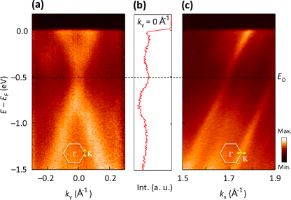
Interestingly, however, single-layer graphene on metallic substrates Varykhalov ; Vita , i. e. , the case where dielectric screening is further enhanced, does not show the characteristic feature of the screened plasmaron bands, but exhibits a dip at in the EDC. Figure 5 shows ARPES intensity maps of single-layer graphene on a Cu film. Along both perpendicular (Fig. 5(a)) and parallel (Fig. 5(c)) to the direction of the graphene unit cell denoted in the inset, the graphene bands show weak spectral intensity (or a dip in the EDC) at in contrast to the high spectral intensity observed at of single-layer graphene on an SiC substrate.
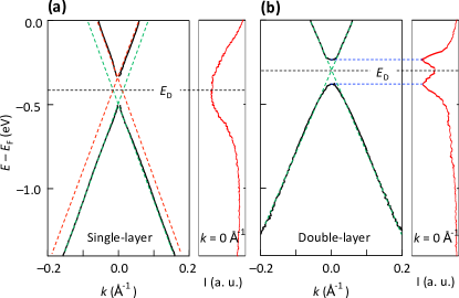
Instead, the spectral feature observed from graphene on metallic substrates Varykhalov ; Vita resembles that of double-layer graphene. At , determined by the crossing point of the green dashed lines drawn along the fitted bands in Fig. 4(b), the EDC shows a dip in between two peaks corresponding to the conduction band minimum and the valence band maximum (as denoted by blue dashed lines). This indicates that our double-layer graphene sample does not show the characteristic feature of the plasmaron bands reported in the case of single-layer graphene MacDonald1 ; MacDonald2 ; Eli1 ; Eli2 . However, not only single-layer graphene, but also double-layer graphene is predicted to exhibit the plasmaron bands in the presence of charge imbalance between the adjacent layers Phan , which is intrinsically induced in epitaxial double-layer graphene on an SiC(0001) substrate Ohta as shown in Fig. 2(e). In addition, for single-layer graphene, the separation between the extended lines and the conduction (or valence) band is 9514 meV, which is bigger than our experimental resolution, 32 meV, as much as by a factor of 3. This means that the additional feature, if any, e. g. , the plasmaron bands MacDonald1 ; MacDonald2 , should be resolved within our experimental resolution. In reality however, we do not observe two separated bands corresponding to the graphene bands and plasmaron bands. These two observations cast doubt on the description of the high spectral intensity at of single-layer graphene on an SiC(0001) substrate in terms of the plasmaron bands Eli1 . In fact, a recent theoretical study suggests the absence of the well-defined plasmaron bands in the epitaxial doped single-layer graphene on the SiC substrate Louie .
The high spectral intensity at can be alternatively explained by the in-gap states accompanied by the energy gap opening. The presence of the buffer layer under single-layer graphene can break sublattice symmetry resulting in the energy gap opening at Zhou07 . At the same time, the localized states of the buffer layer are predicted to couple with the graphene bands resulting in finite spectral intensity in the gap region of single-layer graphene Kim . Within this picture, the spectral intensity of the localized states is expected to gradually decrease with the evolution of graphene overlayers, consistent with our observations shown in Figs. 2 and 3. In addition, when for single- and double-layer graphene is different, the spectral intensity of the in-gap states is not expected to contribute to the spectral intensity at of double-layer graphene. In fact, is 0.43 eV and 0.30 eV below for single- and double-layer graphene, respectively, as shown in Figs. 4(a) and 4(b), and the in-gap states (or the high spectral intensity) lies near 0.43 eV (Fig. 4(a)) below which is close to the valence band maximum of double-layer graphene denoted by the lower blue dashed line in Fig. 4(b). These are exactly what we have manifested in Figs. 2-4.
IV Summary
We have investigated electron band structure of buffer layer, single- and double-layer graphene samples epitaxially grown on an SiC(0001) substrate. The spectral intensity of the non-dispersive states originating from the localized states of the buffer layer decreases with the evolution of double-layer graphene. At the same time, we found that the high spectral intensity at the Dirac energy is observed only for single-layer graphene, whereas double-layer graphene exhibits a dip in spectral intensity in between the conduction band minimum and valence band maximum. Our results suggest that the high spectral intensity observed at of single-layer graphene is well described by the in-gap states picture, in which the buffer layer states are coupled to the graphene bands giving rise to a finite contribution in the spectral intensity at Kim , while the plasmaron bands picture does not explain different spectral intensity observed at of single- and double-layer graphene.
Acknowledgements.
This work was supported by Basic Science Research Program through the National Research Foundation of Korea (NRF) funded by the Ministry of Science, ICT & Future Planning (No. 2015R1C1A1A01053065).References
References
- (1) Castro Neto A H, Guinea F, Peres N M R, Novoselov K S and Geim A K 2009 Rev. Mod. Phys. 81 110
- (2) Hwang C, Siegel D A, Mo S -K, Regan W, Ismach A, Zhang Y, Zettl A and Lanzara A 2012 Sci. Rep. 2 590
- (3) Polini M, Asgari R, Borghi G, Barlas Y, Pereg-Barnea T and MacDonald A H 2008 Phys. Rev. B 77 081411(R)
- (4) Principi A, Polini M, Asgari R and MacDonald A H 2012 Sol. State Commun. 152 1456
- (5) Bostwick A, Speck F, Seyller Th, Horn K, Polini M, Asgari R, MacDonal A H and Rotenberg E 2010, Science 328 999
- (6) Walter A L, Bostwick A, Jeon K -J, Speck F, Ostler M, Seyller Th, Moreschini L, Chang Y J, Polini M, Asgari R, MacDonald A H, Horn K and Rotenberg E 2011 Phys. Rev. B 84 085410
- (7) Lischner J, Vigil-Fowler D and Louie S G 2013 Phys. Rev. Lett. 110 146801
- (8) Varchon F, Feng R, Hass J, Li X, Ngoc Nguyen B, Naud C, Mallet P, Veuillen J -Y, Berger C, Conrad E H and Magaud L 2007 Phys. Rev. Lett. 99 126805
- (9) Kim S, Ihm J, Choi H J and Son Y -W 2008 Phys. Rev. Lett. 100 176802
- (10) Lee S -H, Chung H -J, Heo J, Yang H, Shin J, Chung U -I and Seo S 2011 ACS Nano 5 2964
- (11) Zhou S Y, Gweon G -H, Fedorov A V, First P N, De Heer W A, Lee D -H, Guinea F, Castro Neto A H and Lanzara A 2007 Nat. Mater. 6 770
- (12) Rusponi S, Papagno M, Moras P, Vlaic S, Etzkorn M, Sheverdyaeva P M, Pacilé D, Brune H and Carbone C 2010 Phys. Rev. Lett. 105 246803
- (13) Phan V -N and Fehske H 2012 New J. Phys. 14, 075007
- (14) Rollings E, Gweon G -H, Zhou S Y, Mun B S, McChesney J L, Hussain B S, Fedorov A V, First P N, de Heer W A and Lanzara A 2006 J. Phys. Chem. Solids 67 2172
- (15) Kim K S, Zhao Y, Jang H, Lee S Y, Kim J M, Kim K S, Ahn J -H, Kim P, Choi J -Y and Hong B H 2009 Nature 457 706
- (16) Emtsev K V, Seyller Th, Speck F, Ley L, Stojanov P, Riley J D and Leckey R G C 2006 Mater. Sci. Forum 556-557 525
- (17) Seyller Th, Emtsev K V, Speck F, Gao K -Y and Ley L 2006 Appl. Phys. Lett. 88 242103
- (18) Siegel D A, Zhou S Y, El Gabaly F, Fedorov A V, Schmid A K and Lanzara A 2008 Appl. Phys. Lett. 93 243119
- (19) Ugeda M M, Bradley A J, Shi S -F, da Jornada F H, Zhang Y, Qiu D Y, Ruan W, Mo S -K, Hussain Z, Shen Z -X, Wang F, Louie S G and Crommie M F 2014 Nat. Mater. 13 1091
- (20) Zhang Y, Chang T -R, Zhou B, Cui Y -T, Yan H, Liu Z, Schmitt F, Lee J, Moore R, Chen Y, Lin H, Jeng H -T, Mo S -K, Hussain Z, Bansil A and Shen Z -X 2014 Nat. Nano. 9 111
- (21) Ohta T, Bostwick A, Seyller Th, Horn K and Rotenberg E 2006 Science 313 951
- (22) Varykhalov A, Sánchez-Barriga J, Marchenko D, Hlawenka P, Mandal P S and Rader O 2015 Nat. Commun. 6 7610
- (23) Vita H, Bötcher S, Voloshin E N, Ovcharenko R E, Kampen Th, Thesen A and Dedkov Yu S 2014 Sci. Rep. 4 5704