Electronic and magnetic properties of single-layer MPX3 metal phosphorous trichalcogenides
Abstract
We survey the electronic structure and magnetic properties of two dimensional (2D) MPX3 (M= V, Cr, Mn, Fe, Co, Ni, Cu, Zn, and X = S, Se, Te) transition metal chalcogenophosphates to shed light on their potential role as single-layer van der Waals materials that possess magnetic order. Our ab initio calculations predict that most of these single-layer materials are antiferromagnetic semiconductors. The band gaps of the antiferromagnetic states decrease as the atomic number of the chalcogen atom increases (from S to Se to Te), leading in some cases to half-metallic ferromagnetic states or to non-magnetic metallic states. We find that the competition between antiferromagnetic and ferromagnetic states can be substantially influenced by gating and by strain engineering. The sensitive interdependence we find between magnetic, structural, and electronic properties establishes the potential of this 2D materials class for applications in spintronics.
pacs:
75.70.Ak,85.75.Hh,77.80.B-,75.30.Kz,75.50.PpI Introduction
Following seminal studies that reported on the exfoliation of a stable single-layer graphene and on transport measurements with nearly ideal Dirac fermion fingerprints,novoselov_nature ; philipkim_nature research on ultrathin two dimensional (2D) materials has emerged during the last decade as one of the most active research topics in condensed matter physics. Two-dimensional materials are interesting in part because their properties can be modified in situ by adjusting gate voltages. Recently, the focus of 2D materials research has expanded beyond graphene to include other layered van der Waals materials with a variety of distinct physical properties. novoselov_pnas For example, one popular class of 2D materials is the transition metal dichalcogenides (TMDC) chowalla which includes metals, semiconductors with exceptionally strong light-matter coupling, lightmatter and broken symmetry electronic states including ones with charge density wave and superconducting order. tas2 ; tmdneto ; frindt ; mos2sc Magnetic order has, however, not yet been established in any two-dimensional material. Room-temperature magnetism in a single-layer material is an extremely attractive materials target because of the expectation that it might provide unprecedented electrical control of magnetism and enable new classes of information processing devices that incorporate non-volatile memory elements more intimately.
One strategy to search theoretically for magnetism in isolated two-dimensional van der Waals materials is to explore the magnetic properties of single-layers exfoliated from a bulk material that exhibits robust magnetic order. Following this approach, recent theoretical studies have proposed a number of potential magnetic single-layer van der Waals materials, including group-V based dichalcogenides, 2dmagtmd FeBr3, the chromium based ternary tritellurides CrSiTe3 and CrGeTe3, lebegue ; max1 ; max2 ; max3 ; max4 ; max5 ; max6 ; sivadas CrX3 trihalides, cri3 ; crx3 and MnPX3 ternary chalcogenides. niu ; jacs The vanadium based dichalcogenides, VX2 (X=S, Se) were proposed first and are predicted to have strain tunable ferromagnetic phases. 2dmagtmd The trihalides CrX3 (X = F, Cl, Br, I) crx3 are new classes of semiconducting ferromagnet with Curie temperature predictions of TC 100 K.
The bulk ternary tritellurides CrATe3 (A = Si, Ge) max1 were predicted within LDA to be ferromagnetic with small band gaps of 0.04 and 0.06 eV respectively. Their few layers limits have recently been studied in temperature dependent transport experiments. max6 The anisotropy along the c-axis and the dynamic correlations in the ab-plane seen by elastic and inelastic neutron scattering are characteristic of 2D magnetism. max3 In the single layer limit CrSiTe3 is a semiconductor with a GGA gap of 0.4 eV, max5 substantially larger than its bulk value, and has a negative thermal expansion. max2 Reports differ on the most stable magnetic phase between ferromagnetic max1 ; max2 ; max5 or antiferromagnetic. sivadas For larger atomic number compounds like CrGeTe3 and CrSnTe3, DFT predicts ferromagnetic semiconducting phases with Curie temperatures between 80-170K. sivadas ; max4 ; max6
We focus here on single-layer materials formed from compounds in the transition metal phosphorous trichalcogenide (MPX3) family, which are known to exhibit magnetism for M=Mn and for a number of other metal atom species. Metal phosphorous trichalcogenides are cousins of CrSiTe3, but are so far less studied for 2D magnetism. According to one recent study monolayer MnPSe3 and MnPS3 exhibit Neel antiferromagnetism jacs and valley-dependent optical properties. niu The structures and magnetic properties of some bulk compounds from this family have already been extensively studied. mpx3struct1 ; wildes ; mpx3struct2 ; mpx3struct3 ; mpx3struct4 ; mpx3struct5 ; mpx3mag1 ; mpx3mag2 ; mpx3mag3 ; mpx3mag4 ; mpx3mag5 ; mpx3mag6 ; mpx3mag7 ; mpx3mag8 ; mpx3mag9 ; mpx3mag10 ; mpx3mag11 ; mpx3mag12 ; mpx3mag13 ; mpx3mag14 ; mpx3other15 ; mpx3other16 ; mpx3other16b ; mpx3other16c ; mpx3other17 ; mpx3other18 Because of the van der Waals character of these materials, one focus of bulk materials research is to characterize ion intercalation properties. mpx3inter1 ; mpx3inter2 ; mpx3inter3 ; mpx3inter4 ; mpx3inter5 For 2D magnetic materials to be most useful in device applications it is desirable to seek pathways to increase the critical temperature at which they order magnetically. We compare theoretical predictions for a variety of late 3d transition metals (M= V, Cr, Mn, Fe, Co, Ni, Cu, Zn) and consider all there chalcogen atoms (X = S, Se, Te) in an effort to explore the magnetic phases that can be expected as fully as possible. We study how the electronic bands are modified when the magnetic state undergoes a transition from antiferromagnetic to ferromagnetic, or from magnetic to non-magnetic. Our results confirm the expected strong interdependence between magnetism and structural properties, for example lattice constant and crystal symmetry, and explain a surprisingly strong dependence of exchange interaction strengths on electron density and strain. Because these materials may have relatively strong correlations, ab initio density-functional theory is not able to make quantitatively reliable predictions for all properties. Nevertheless our survey provides considerable insight into materials-property trends, and into the potential for engineering the magnetic properties of these materials using field effects and strain engineering.
Our paper is structured in the following manner. We start in Sec. II by briefly summarizing some specific details of our first principles electronic structure calculations. In Sec. III we discuss our results for ground-state properties including structure, magnetic properties, and electronic band structures and densities-of-states. Sec. IV is devoted to an analysis of the carrier-density dependence of the magnetic ground state, and to a study of the influence of strain on the magnetic phase diagram. Finally we close the paper in Sec.V with a summary and discussion of our results.
II Ab initio calculation details
The study of the ground-state electronic structure and magnetic properties in this work has been carried out using plane-wave density functional theory as implemented in Quantum Espresso. espresso We have used the Rappe-Rabe-Kaxiras-Joannopoulos ultrasoft (RRKJUS) pseudoptentials for the semi-local Perdew-Burke-Ernzerhof (PBE) generalized gradient approximation (GGA) GGA together with the VdW-D2 correction d2grimme . We choose the GGA+D2 as a reference calculation because of the overall improvement of the GGA over the LDA LDA for covalent bond description, and add the longer ranged D2 correction to improve the description of binding between the layers. (The GGA typically performs poorly for van der Waals bonds. noamarom ) The magnetic solutions have also been compared with calculations employing the DFT+U scheme, using the same value of eV and alternatively using onsite repulsion values that saturate the magnitude of the band gap. Comparisons were made with hybrid HSE+D2 functionals hse to assess non-local exchange effects that could further influence the magnetic ground states. All structures were optimized without constraints until the forces on each atom reached 10-5 Ry/au. The self-consistency criteria for total energies has been set at 10-10 Ry and momentum space integrals were performed using a regularly spaced k-point sampling density of 16161 for the triangular lattice case and 1681 for the rectangular lattice case, with a plane wave energy cutoff between 60 to 90 Ry. For the HSE+D2 calculation we used a coarser effective k-point sampling of 441. The out-of-plane vertical size of the periodic supercell was chosen to be 25 , which typically leaves an adequate vacuum spacing greater than 10 between two-dimensional layers.
III Structural and magnetic properties
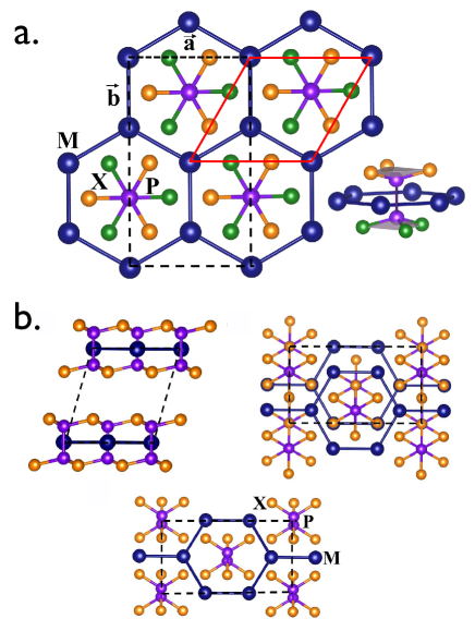
The atomic structure of MPX3 transition metal chalcogenophosphate layers is anchored by (P2X6)4- bipyramids arranged in a triangular lattice that provide enclosures for transition metal atoms. (See Fig. 1 for a schematic illustration of the single layer unit cell and the bulk atomic structure.) The bulk crystals consists of ABC-stacked single layer assemblies that are held together by van der Waals forces. Although the atomic structures of single layer transition metal phosphorous trichalcogenide crystals are similar to those of bulk crystals, small changes appear in response to the absence of the interlayer coupling, with distortions in the ground-state crystal geometries correlated mainly with the magnetic phase. The analysis of magnetic properties is simplified by the fact that the magnetic moments develop almost entirely at the metal atom sites.
We calculate the magnetic ground-state and meta-stable magnetic configurations by identifying the energy extrema obtained by iterating self-consistent field equations to convergence starting from magnetic initial conditions that can be classified as either Néel antiferromagnetic (AFM), or ferromagnetic (FM), or nonmagnetic (NM) states. The calculation indicates that most 2D MPX3 crystals are semiconductors with localized magnetic moments that are ordered antiferromagnetically. We find that the use of chalcogen atoms with larger atomic numbers tends to yield smaller energy gaps between valence and conduction bands. In the following we present an analysis of the structural and magnetic properties of representative 3d transition metal MPX3 trichalcogenides, and discuss their underlying electronic band structures.

III.1 Structural properties
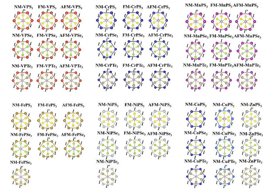
The MPX3 compounds that we study consist of V, Cr, Mn, Fe, Co, Ni, Cu, and Zn transition metal atoms with 3d valence electrons, combined with three different chalcogen atoms S, Se, and Te. We thus expand our study beyond the most common crystals in this class, the MnPS3, FePS3, CoPS3, NiPS3, ZnPS3 thiophosphates whose bulk structure had been explored in past experiments. mpx3struct1 ; mpx3struct2 ; mpx3struct3 ; mpx3struct4 ; mpx3struct5 ; mpx3mag1 ; mpx3mag2 ; mpx3mag3 ; mpx3mag4 ; mpx3mag5 ; mpx3mag6 ; mpx3mag7 ; mpx3mag8 ; mpx3mag9 ; mpx3mag10 ; mpx3mag11 ; mpx3mag12 ; mpx3inter2 ; mpx3inter3 ; mpx3inter4 ; mpx3inter5 We have optimized MPX3 lattice structures using the unit cell shown in Fig. 1 for single layers and assuming ABC stacking for bulk. Given this framework, structures are characterized by the value of the in-plane lattice constant , the (P-P) distance between the phosphorous atoms, the (M-M) distance between metal atoms, and the (P-X) distance between phosphorous atoms and chalcogen atoms. The variation in the magnitude of these bond lengths as a function of the metal and chalcogen atom species, and magnetic configuration is illustrated in Fig. 2, and summarized numerically in Table II in the Supplemental Material. Results are presented for all metastable magnetic states. The structures have a simple dependence on chalcogen atom size, with larger in-plane lattice constants and monolayer thicknesses (P-P distances) for larger chalcogens. However, the dependence of structure on metal atom atomic number is not straightforward. Experiments in the bulk MPS3 observed a close correlation between the radius of the metal cation and the P-P distance of the thiophosphate bipyramid.mpx3struct1 The non-monotonic variation of the metal cation radius with respect to atomic number is reflected in the P-P distance trend. However, our calculations show that bond lengths correlate more strongly with magnetic state than with metal atomic number.
| MPX3 | X | NM | FM | AFM | |||
|---|---|---|---|---|---|---|---|
| a(Å) | c′(Å) | a(Å) | c′(Å) | a(Å) | c′(Å) | ||
| S | 5.737 | 3.142 | 5.880 | 3.166 | 5.846 | 3.170 | |
| S(bulk) | 5.742 | 3.280 | 5.918 | 3.273 | 5.845 | 3.294 | |
| (2.518) | (2.585) | (2.655) | |||||
| S(Expt) | |||||||
| VPX3 | Se | 6.123 | 3.266 | 6.230 | 3.204 | 6.214 | 3.318 |
| Te | 6.885 | 3.328 | 6.935 | 3.418 | 6.980 | 3.431 | |
| S | 5.851 | 3.071 | 5.914 | 3.032 | 5.885 | 3.336 | |
| S(bulk) | 5.862 | 3.116 | 5.913 | 3.185 | 5.934 | 3.301 | |
| (2.624) | (2.506) | (2.465) | |||||
| S(Expt) | |||||||
| CrPX3 | Se | 6.035 | 3.367 | 6.320 | 3.100 | 6.325 | 3.235 |
| Te | 6.530 | 3.672 | 6.880 | 3.330 | 6.804 | 3.388 | |
| S | 5.780 | 2.952 | 6.023 | 3.256 | 5.997 | 3.246 | |
| S(bulk) | 5.787 | 2.875 | 6.018 | 3.125 | 5.993 | 3.268 | |
| (2.456) | (2.567) | (2.562) | |||||
| S(Expt) | 6.076 | ||||||
| MnPX3 | Se | 6.045 | 3.182 | 6.340 | 3.416 | 6.334 | 3.402 |
| Te | 6.530 | 3.444 | 6.805 | 3.550 | 6.874 | 3.535 | |
| S | 5.730 | 2.808 | 5.891 | 3.150 | 5.958 | 3.180 | |
| S(bulk) | 5.736 | 2.969 | 5.874 | 3.313 | 5.921 | 3.217 | |
| (2.386) | (2.840) | (4.368) | |||||
| S(Expt) | 5.934 | ||||||
| FePX3 | Se | 6.130 | 2.911 | 6.134 | 3.347 | 6.239 | 3.214 |
| Te | 6.676 | 3.038 | |||||
| S | 5.763 | 2.790 | |||||
| S(bulk) | 5.784 | 2.950 | |||||
| (4.250) | |||||||
| S(Expt) | 5.901 | ||||||
| CoPX3 | Se | 6.186 | 2.850 | ||||
| Te | 6.772 | 3.057 | |||||
| S | 5.766 | 2.974 | 5.792 | 3.064 | 5.783 | 3.042 | |
| S(bulk) | 5.763 | 2.995 | 5.789 | 3.062 | 5.779 | 3052 | |
| (2.431) | (2.449) | (2.480) | |||||
| S(Expt) | 5.813 | ||||||
| NiPX3 | Se | 6.132 | 3.086 | 6.134 | 3.100 | 6.140 | 3.142 |
| Te | 6.700 | 3.208 | |||||
| S | 5.837 | 3.439 | |||||
| S(bulk) | 5.843 | 2.245 | |||||
| (3.903) | |||||||
| S(Expt) | |||||||
| CuPX3 | Se | 6.151 | 3.532 | ||||
| Te | 6.711 | 3.617 | |||||
| S | 5.966 | 3.230 | |||||
| S(bulk) | 5.973 | 2.564 | |||||
| (3.025) | |||||||
| S(Expt) | 5.971 | ||||||
| ZnPX3 | Se | 6.323 | 3.379 | ||||
| Te | 6.871 | 3.597 |
P-P distances range between 2.152.3 while M-M bond lengths vary by about 5% . The M-M bond lengths within an hexagon can be unequal, distorting the hexagonal lattice arrangement of the metal atoms as illustrated in Fig. S1 in the Supplemental MaterialSI . In general ferromagnetic states have the largest lattice constants, and antiferromagnets have intermediate lattice constants. The fact that the structural properties of these crystals are correlated with their magnetic configurations suggests the possibility of controlling magnetic properties by straining the lattice, as we will discuss more in detail in a later section.
The comparison between lattice parameters calculated with GGA+D2 and the experimental bulk structure is summarized in Table 5. The comparison of the GGA and LDA lattice parameters in Table I of the Supplemental Material indicates important discrepancies between the GGA and LDA, and is consistent with the tendency of the LDA to overbind covalent bonds. The stronger LDA bonds leads to a global reduction of lattice constant and to a stronger distortion of the metal honeycombs. Within the LDA we find optimized lattice parameters that are (2-5) shorter than in bulk experiments. The GGA agreement is good (0.5-1.6%) for MnPS3, FePS3, CoPS3, NiPS3 and ZnPS3.
III.2 Magnetic properties
| MPX3 | X | Rectangular | Triangular | Work function (eV) | ||||||||
|---|---|---|---|---|---|---|---|---|---|---|---|---|
| NM | FM | AFM | zAFM | sAFM | NM | FM | AFM | NM | FM | AFM | ||
| S | 1142.8 | 643.2 | 0.0 | 246.9 | 132.7 | 1083.8 | 695.8 | 0.0 | 3.56 | 3.26 | 3.42 | |
| VPX3 | Se | 906.9 | 275.8 | 0.0 | 164.6 | 87.78 | 1348.1 | 458.8 | 0.0 | 2.82 | 3.57 | 3.58 |
| Te | 0.0 | 399.3 | 323.9 | 371.4 | 327.9 | 1296.5 | 183.1 | 0.0 | 3.08 | 3.88 | 3.85 | |
| S | 1454.5 | 0.0 | 91.65 | 30.62 | 63.23 | 1182.5 | 0.0 | 73.68 | 3.40 | 3.07 | 3.62 | |
| CrPX3 | Se | 1514.6 | 0.0 | 146.1 | 57.06 | 522.7 | 1293.7 | 0.0 | 315.4 | 3.98 | 3.52 | 3.65 |
| Te | 1373.4 | 0.0 | 242.9 | 81.31 | 12.06 | 1482.6 | 0.0 | 264.2 | 3.74 | 3.55 | 3.41 | |
| S | 1576.2 | 186.3 | 0.0 | 60.68 | 74.59 | 1964.1 | 205.4 | 0.0 | 3.74 | 4.41 | 3.98 | |
| MnPX3 | Se | 1356.6 | 156.7 | 0.0 | 48.96 | 68.98 | 1417.3 | 166.4 | 0.0 | 3.98 | 4.07 | 3.91 |
| Te | 0.0 | 840.0 | 12.44 | 0.0 | 3.68 | 3.66 | 3.77 | |||||
| S | 141.5 | 286.8 | 115.8 | 0.0 | 289.0 | 44.87 | 0.0 | 308.3 | 3.41 | 4.13 | 4.23 | |
| FePX3 | Se | 0.0 | 0.0 | 165.0 | 324.5 | 3.93 | 3.73 | 3.86 | ||||
| Te | 0.0 | 0.0 | 3.32 | |||||||||
| S | 0.0 | 0.0 | 3.84 | |||||||||
| CoPX3 | Se | 0.0 | 0.0 | 4.33 | ||||||||
| Te | 0.0 | 0.0 | 3.50 | |||||||||
| S | 507.5 | 276.7 | 64.16 | 0.0 | 343.5 | 425.1 | 213.4 | 0.0 | 4.63 | 4.91 | 5.08 | |
| NiPX3 | Se | 324.8 | 196.2 | 0.0 | 383.2 | 278.2 | 168.0 | 158.8 | 0.0 | 4.79 | 4.54 | 4.44 |
| Te | 0.0 | 0.0 | 2.58 | |||||||||
| S | 0.0 | 0.0 | 4.96 | |||||||||
| CuPX3 | Se | 0.0 | 0.0 | 5.15 | ||||||||
| Te | 0.0 | 0.0 | 2.96 | |||||||||
| S | 0.0 | 0.0 | 3.97 | |||||||||
| ZnPX3 | Se | 0.0 | 0.0 | 4.47 | ||||||||
| Te | 0.0 | 0.0 | 1.11 | |||||||||
Experimental studies of the magnetic properties of bulk Mn, Fe, Co, Ni thiophosphates have found antiferromagnetic ground states with Néel temperatures ranging between 82K155K. mpx3struct1 ; wildes Here we find that magnetism persists in single layer MPX3 compounds. The magnetic moments develop mainly at the localized metal atom sites, except for a noticeable spin polarization that develops on the phosphorous and sulphur atom sites in the ferromagnetic configuration.
The late 3d transition elements Cr, Mn, Fe, Co and Ni stand out in the periodic table as elements that tend to order magnetically. The bonding arrangements of particular compounds can however enhance or suppress magnetism. In 2D MPX3 crystals, transition metal atoms are contained within phosphorous trichalcogenide bipyramidal cages, and have weak direct hybridization with other transition metal atoms. The exchange interactions between the metal atoms are therefore mainly mediated by indirect exchange through the intermediate chalcogen and P atoms. Magnetic interactions can be extracted from ab initio electronic structure calculations by comparing the ground state energies of different magnetic configurations. We compare the energies of antiferromagnetic, ferromagnetic, and nonmagnetic states in V, Cr, Mn, Fe, Ni based compounds in Table 8, where we find that the AFM phase is normally favored over the FM phase.
Because our calculations show that the magnetic moments are concentrated at the metal atoms sites we can characterize the magnetic properties of 2D MPX3 compounds by mapping the energy landscape to an effective classical spin Hamiltonian on a honeycomb lattice:
| (1) |
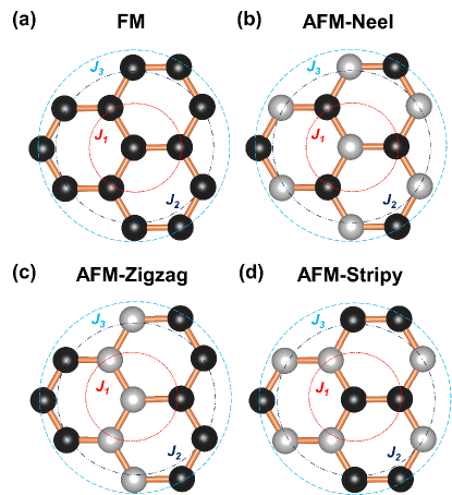
where is the total spin magnetic moment of the atomic site , is the exchange coupling parameters between two local spins, and the prefactor 1/2 accounts for the double-counting. The estimated magnetic anisotropy energies that we obtained from non-collinear magnetization calculations are on the order of 160 eV per formula unit for the FM compounds CrPS3, CrPSe3 and on the order of 1000 eV per formula unit for the AFM compounds MnPS3, MnPSe3 with magnetization favored perpendicular to the plane. For this reason, in making the estimates that we describe below, we take the Ising limit of this spin-Hamiltonian. By evaluating the three independent energy differences between the four magnetic configurations mpx3struct1 ; chaloupka ; sivadas illustrated in Fig. 3, ferromagnetic (FM), Néel (AFM), zigzag AFM (zAFM), and stripy AFM (sAFM), and assuming that the magnetic interactions are short range, we can extract the nearest neighbor (), second neighbor (), and third neighbor () coupling constants:sivadas
| (2) | |||||
| (3) | |||||
| (4) |
where is the average spin magnetic moment on the honeycomb sublattice . The total energies of the zAFM and sAFM magnetic configurations, which must be calculated using a rectangular supercell, usually have higher energies than the average of the AFM solutions and FM solutions. The larger rectangular unit cell required for describing more complex zAFM and sAFM spin configurations imposes certain symmetries that restricts the relaxation of the lattices when compared to the triangular unit cell. For the case of FePS3, however, the zAFM has the lowest energy. The average magnetic moment at each lattice site obtained within the GGA+D2 and GGA+D2+U are listed in Table 3.
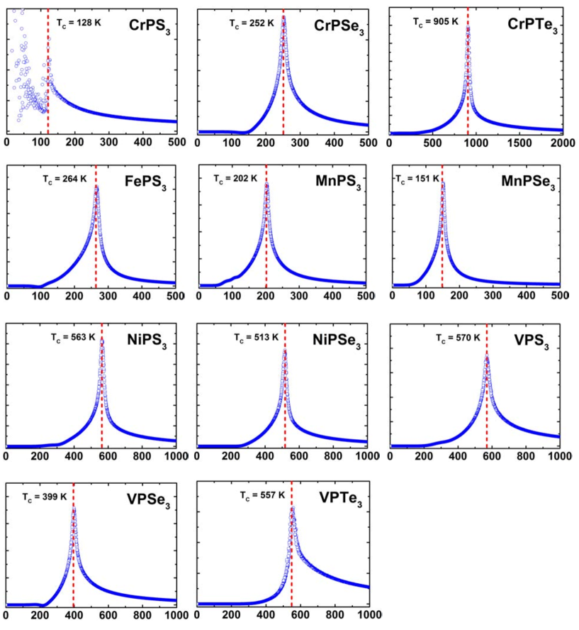
Single-layer magnetic ordering temperatures Tc were estimated by running Monte Carlo simulations of the three-coupling-constant effective models using the Metropolis algorithm in lattice sizes up to =3264 with periodic boundary conditions, metropolis ; newman ; landau and verified against calculations performed using Wang-Landau Monte Carlo sampling algorithm in smaller =816 lattices.wanglandau We calculated the heat capacity as a function of temperature and identified its diverging point as the Neel and Curie temperatures. See the Supplemental MaterialSI for the plot of the representative results for the temperature dependent heat capacity.
| MPX3 | X | Bulk | GGA+D2 | GGA+D2 + U | |||||||||||||||
| FM | AFM | FM | AFM | zAFM | sAFM | Tc | FM | AFM | zAFM | sAFM | Tc | ||||||||
| S | 2.03 | 2.00 | 1.92 | 2.01 | 1.68 | 1.76 | 24.5 | 4.26 | 3.24 | 1100 | 2.96 | 2.93 | 2.95 | 2.93 | 3.93 | 0.147 | 0.143 | 570 | |
| VPX3 | Se | 2.02 | 2.13 | 1.77 | 2.14 | 10.2 | 0.340 | 0.437 | 760 | 2.56 | 2.99 | 3.01 | 2.98 | 2.81 | 0.132 | 0.170 | 400 | ||
| Te | 2.22 | 2.16 | 2.06 | 2.19 | 9.63 | -3.59 | -7.07 | 570 | 3.10 | 3.08 | 3.13 | 3.08 | 5.10 | -1.68 | -3.51 | 560 | |||
| S | 2.83 | 3.07 | 2.85 | 3.14 | 2.37 | 2.34 | -1.73 | -0.015 | 0.029 | 280 | 3.94 | 4.03 | 3.93 | 4.11 | 1.34 | -0.064 | -0.490 | 130 | |
| CrPX3 | Se | 2.77 | 2.83 | 2.45 | 2.38 | -9.82 | -3.49 | 6.62 | 1080 | 4.14 | 4.03 | 4.04 | 4.11 | 0.608 | -0.254 | -3.05 | 250 | ||
| Te | 2.92 | 2.88 | 2.82 | 2.48 | -4.89 | 0.006 | -0.087 | 750 | 4.25 | 4.17 | 4.17 | 4.21 | 0.849 | 0.333 | -2.10 | 900 | |||
| MnPX3 | S | 4.24 | 4.15 | 4.26 | 4.16 | 3.82 | 3.83 | 1.21 | 0.180 | 0.536 | 500 | 4.56 | 4.54 | 4.54 | 4.55 | 0.369 | 0.0284 | 0.152 | 200 |
| Se | 4.25 | 4.20 | 4.24 | 3.82 | 0.958 | 0.136 | 0.506 | 450 | 4.56 | 4.54 | 4.55 | 4.56 | 0.231 | 0.021 | 0.141 | 150 | |||
| FePX3 | S | 3.32 | 3.14 | 3.33 | 3.20 | 3.24 | 2.48 | -1.59 | -0.179 | 3.00 | 690 | 3.48 | 3.46 | 3.48 | 3.47 | 0.575 | 0.140 | 0.69 | 260 |
| NiPX3 | S | 1.25 | 1.13 | 1.26 | 1.14 | 1.12 | 1.20 | -11.3 | -0.115 | 36.0 | 1110 | 1.21 | 1.17 | 1.22 | 1.19 | -4.11 | 1.95 | 17.4 | 560 |
| Se | 0.54 | 0.94 | 0.12 | 0.99 | 127 | -82.3 | -67.6 | 2580 | 1.14 | 1.08 | 1.22 | 1.14 | -3.11 | 1.04 | 18.2 | 510 | |||
The calculated average values of the magnetic moments in the AFM configuration vary widely, assuming the values 2.01, 3.14, 4.16, 3.2, 0.8 and 1.14 for V, Cr, Mn, Fe, Co and Ni based sulphides. (See Table 3). The magnitudes of the magnetic moments at the metal atoms generally have relatively small differences between different magnetic configurations, between 3%10%, while larger variations are found in CoPS3 and NiPSe3. Within GGA+D2 approximation we find that the magnetic moments in 2D MPX3 develop almost entirely at the metal atom sites. In comparison the phosphorous and chalcogens in the bulk structure do acquire a small spin polarization that can be attributed to interlayer coupling. The use of onsite U introduces a small spin polarization enhancement at non-metal atom sites.
III.3 Band structure and density of states
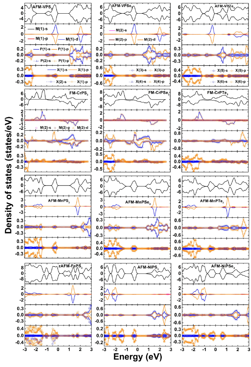
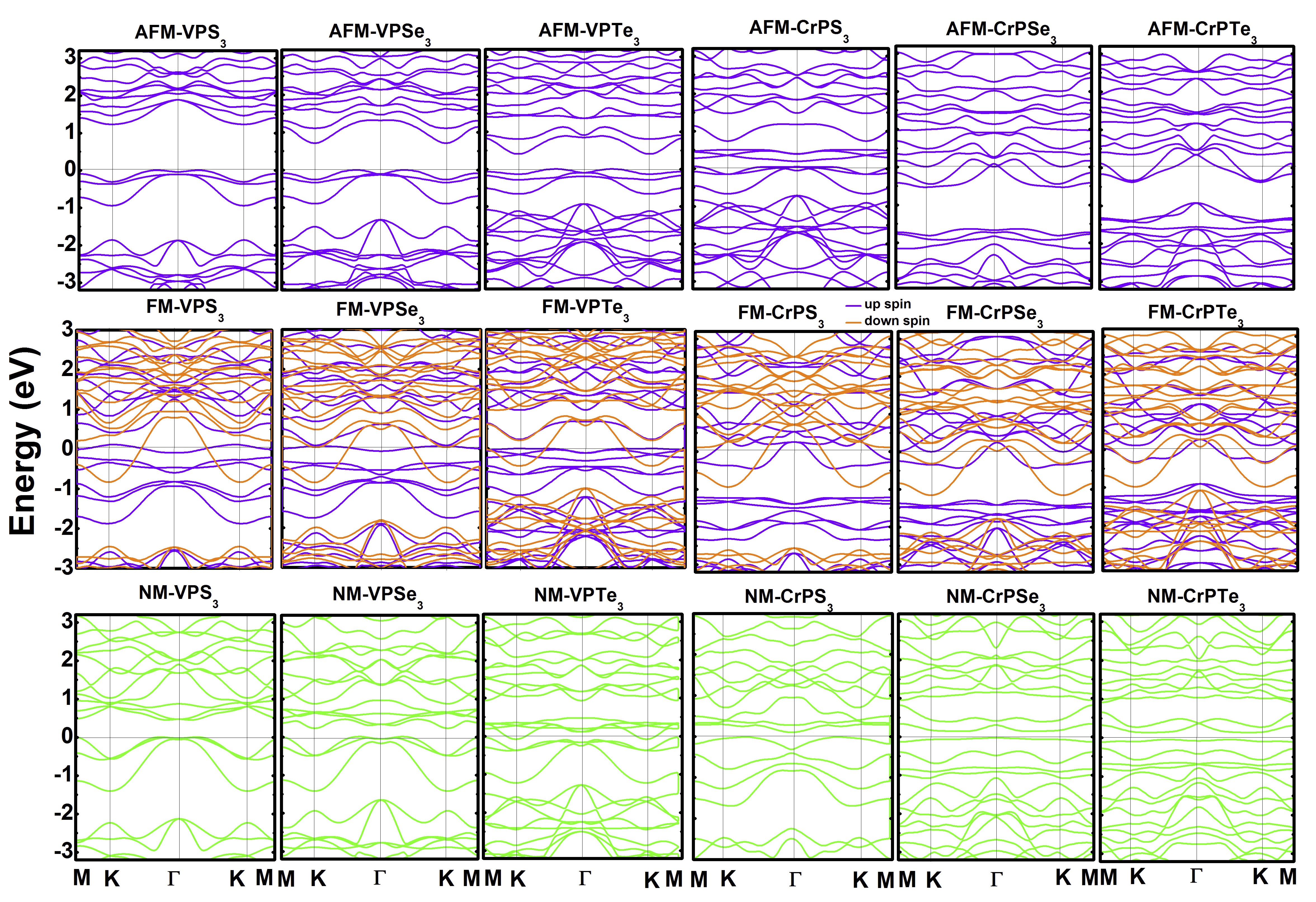
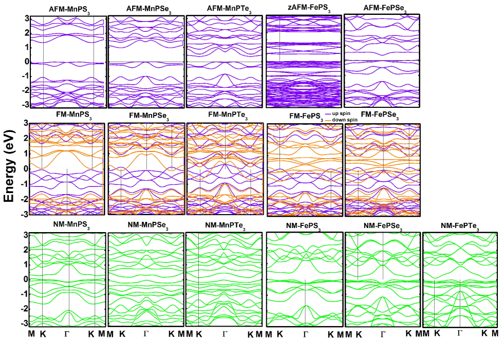
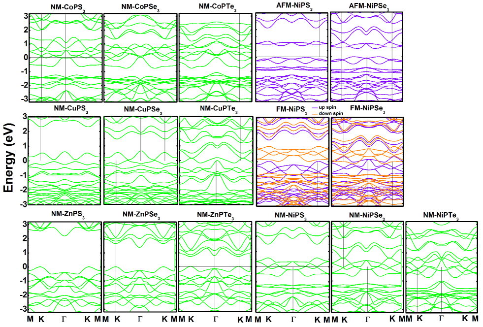
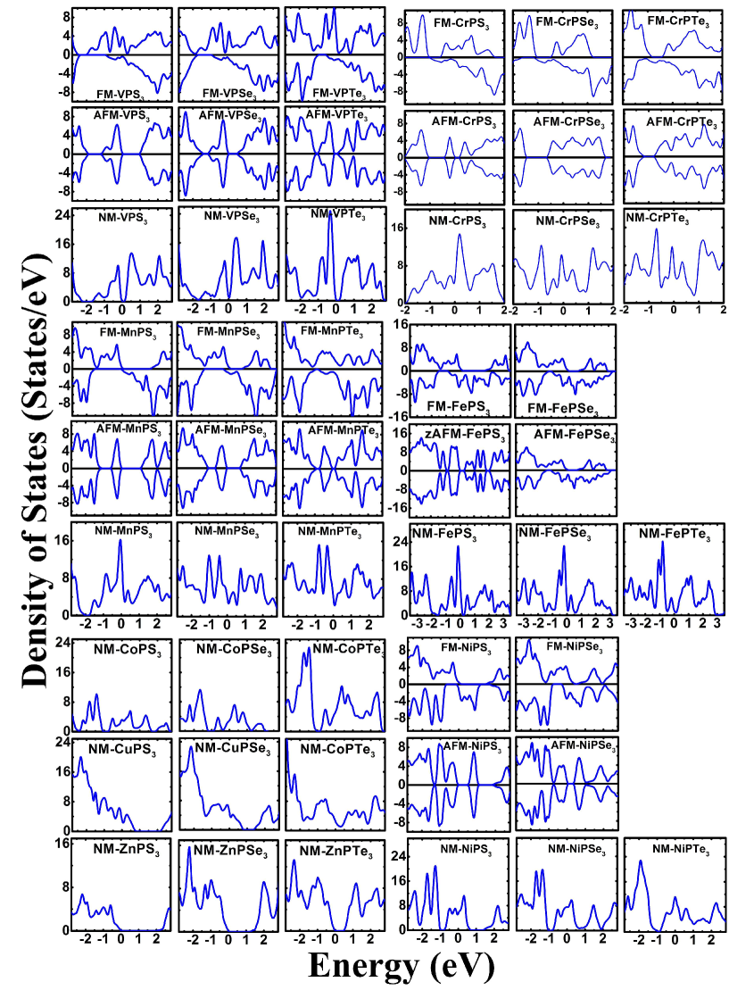
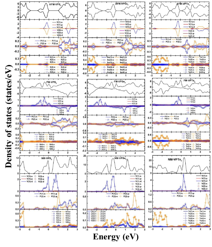
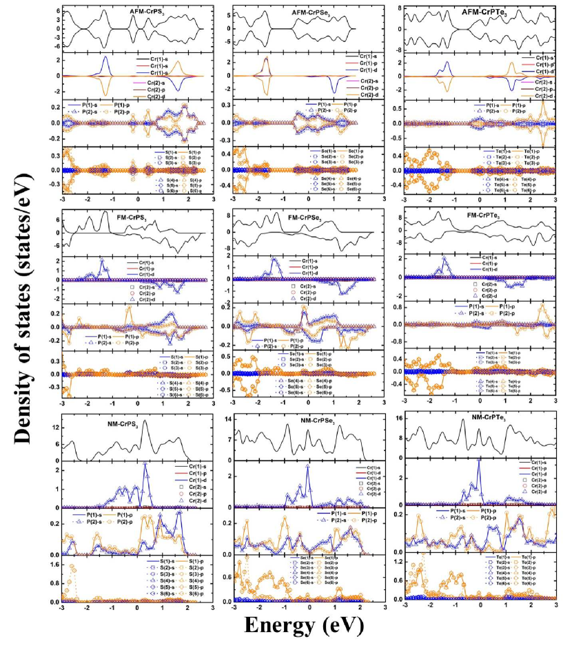
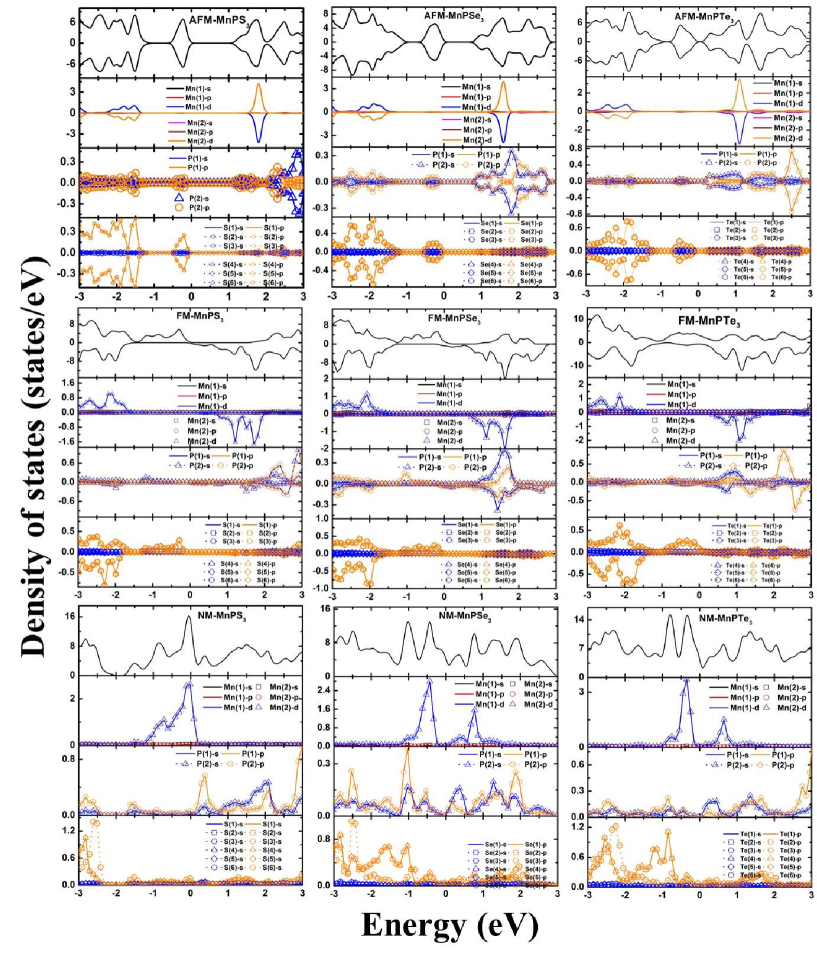
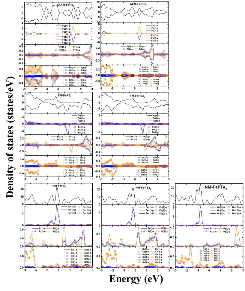
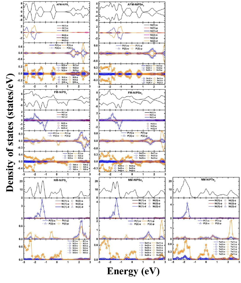
Understanding the electronic properties of 2D MPX3 layers is an essential stepping stone on the path toward possible integration in nanodevices. For spintronic applications of magnetic 2D materials, which seek to couple charge and spin degrees of freedom, it is desirable to understand how the electronic structure depends on the type of magnetic order. The spin resolved band structures of the lowest energy spin configuration, calculated within the GGA+D2 approximation, are presented in Fig. 12, and the associated densities-of-states are presented in Fig. 5, and the projected partial density of states (PDOS) results for various MPX3 compounds presented in Fig. 6. Single layer MPX3 with M = V, Cr, Mn, Fe, Co, Ni, Cu, Zn transition metal atoms and X = S, Se, Te chalcogen atoms are considered. Band structures for higher energy spin configurations are included in the Supplemental MaterialSI .
| X | GGA+D2 | HSE+D2 | GGA+D2+U | |
|---|---|---|---|---|
| S | 1.23 | 2.50 | 2.32 (U = 3.25) | |
| VPX3 | Se | 0.73 | 2.10 | 1.67 (U = 3.25) |
| Te | 0.41 | 1.57 | 1.00 (U = 3.25) | |
| S | 1.36 | 3.05 | 2.34 (U = 5.0) | |
| MnPX3 | Se | 0.98 | 2.24 | 1.70 (U = 5.0) |
| Te | 0.38 | 1.06 | 0.69 (U = 5.0) | |
| S | 0.57 | 2.07 | 2.26 (U = 5.3) | |
| FePX3 | Se | 0.20 | 1.48 | 1.19 (U = 5.3) |
| Te | 0.13 | 1.35 | 0.59 (U = 5.3) | |
| S | 0.84 | 2.83 | 1.74 (U = 6.45) | |
| NiPX3 | Se | 0.59 | 2.22 | 1.31 (U = 6.45) |
| Te | - | 0.27 | - | |
| S | 0.01 | 1.76 | 0.08 (U = 1.0) | |
| CuPX3 | Se | - | 0.56 | - |
| S | 2.19 | 3.11 | 2.23 (U = 5.4) | |
| ZnPX3 | Se | 1.38 | 2.19 | 1.41 (U = 5.4) |
| Te | 0.73 | 1.26 | 0.74 (U = 5.4) |
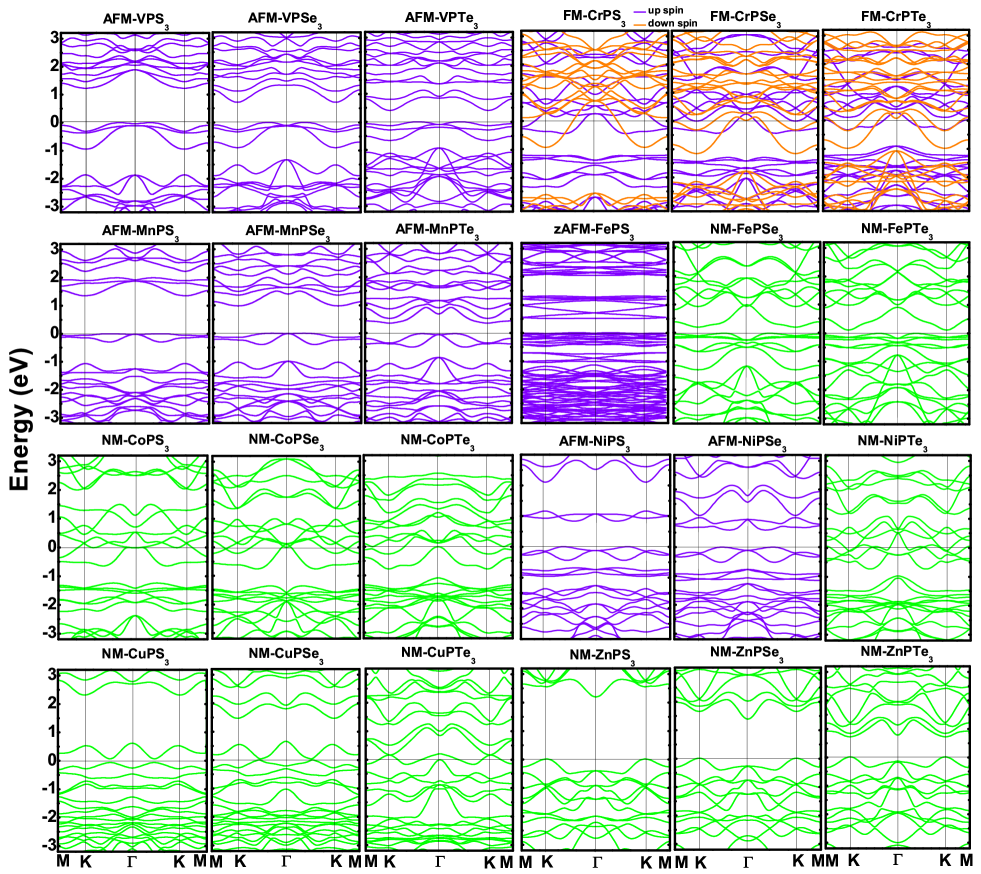
We find that AFMs are almost always gapped semiconductors, that the FM states are metallic, and that the NM phases can be either semiconducting or metallic. It follows that the MPX3 class of materials includes almost all of the behaviors being studied in current spintronics research, including importantly both antiferromagnets and ferromagnets and both metals and insulators.
The AFM band structures for V and Mn based compounds in Fig. 12 show semiconductor behavior and reveal conduction band edges that are near the -points, whereas the valence band edges are between and . This valence bands near the Fermi energy are energetically separated from deeper lying valence bands. We notice from the density of states plot in Fig. 5 that there is strong sensitivity of the electronic structure to the choice of electron-electron interaction model, both for the HSE+D2 approximation containing non-local exchange and for on-site repulsion enhancement introduced through a Hubbard U parameter. The analysis of the orbital projected partial density of states in Fig. 6 for the AFM compounds reveals that the conduction band edges have an important contribution from the s and p orbitals of the P atom while for the valence band edges the chalcogen atom orbitals have an importance presence. Other atoms do contribute near the band edges, e. g. for the V based compounds the d-orbitals are an important fraction of the valence band edge while for the Mn based compounds they lie at deeper energies. We can thus expect that surface functionalization and variations in the carrier density at the surface chalcogens will have a more immediate impact in the valence bands than the conduction bands. The AFM compounds containing Fe and Ni result in non-magnetic solutions when heavier chalcogen atoms are used within our GGA+D2 calculation. The case of FePS3 has as lowest energy configuration the zigzag AFM phase.
For MPX3 compounds the FM configurations are metallic as a general rule. Within our GGA+D2 approximation only the Cr based chalcogenophosphates have FM ground states, while they favor the AFM phase when the onsite U is added, see the Supplemental Material for GGA+D2+U results. We find that the FM configurations are often meta-stable local minima solutions in MPX3 compounds whose lowest energy solutions are AFM. The FM configurations are found in metallic phase at charge neutrality and give rise to half-metallic solutions for MnPS3 and NiPS3. The half-metallicity could be achieved also in MnPSe3 when carrier doped away from neutrality. For the MnPS3 and MnPSe3 compounds we can observe a distinct population of the carriers for the hole and electron sides where doping populate orbitals located at the chalcogen and P atoms respectively.
The electronic properties of NM configurations are also presented in Figs. 12-5. The NM layers could be potentially interesting if magnetic phases could be induced by forming vertical heterojunctions with magnetic materials. Unexpectedly, one typically magnetic element (Co) turns out to be non-magnetic in MPX3 compounds according to our GGA+D2 based calculations. As shown in Fig. 12 the band structure of these non-magnetic materials can be either metallic (Co, Ni, Cu based compounds), semiconducting (Fe), or be a wide gap insulator (Zn).
We now turn our attention to the magnitude of the band gaps of the semiconducting and insulating 2D MPX3 chalcogenophosphates calculated within the GGA approximation, and using other approximations that partially account for Coulomb correlation through non-local exchange or a Hubbard U, are shown in Table 4. These gaps are consistently larger when calculated using the hybrid HSE+D2 approximation which includes non-local exchange in the energy functional. A smaller gap enhancement is obtained using a +U interaction correction. Band gaps are gradually reduced when S is replaced by heavier chalcogen atoms.
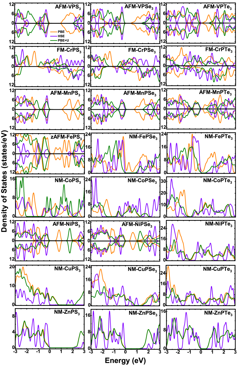
The corresponding density of states (DOS), plotted in Fig. 5, shows the strong influence on the ground-state electronic structure when Coulomb correlations are included. Note in particular the impact of the non-local Coulomb exchange included in the HSE approximation. This suggests that the physics of MPX3 compounds can be dominated by correlation effects and modeling will be most successful when we rely on effective models that feed from experimental input or high level ab initio calculations.
The orbital content of the valence and conduction band edges that are most relevant for studies of carrier-density dependent magnetic properties can be extracted from the orbital projected partial density of states (PDOS) results for various MPX3 compounds presented in Fig. 6. Depending on the specific composition and on the magnetic configuration of the material under consideration, the valence and conduction band edge orbitals can be dominated by metal, phosphorous or chalcogen atoms. A detailed study on the influence of the Coulomb interaction model on the localization properties of the wave functions and their influence on the exchange coupling in MPX3 compounds will be presented elsewhere.
IV Tunability of magnetic properties
Two dimensional magnetic materials are of interest primarily because of the prospect that their properties might be more effectively altered by tuning parameters that are available in situ. Two potentially important control knobs that can be exploited experimentally in two-dimensional-material based nano-devices are carrier-density and strain. The dependence of magnetic properties on carrier density is particularly interesting because it provides a convenient route for electrical manipulation of magnetic properties. In this section we explore the possibility of tailoring the electronic and magnetic properties of MPX3 ultrathin layers by adjusting carrier density or by subjecting the MPX3 layers to external strains.
IV.1 Field-effect modification of magnetic properties
The goal of modifying the magnetic properties of a material simply by applying a gate voltage is a holy grail in magneto-electronics because it could allow magnetically stored information to be written at negligible energy cost. Electric field control of magnetic order has been demonstrated in a number of materials. In ferromagnetic semiconductors the mechanism is carrier density variation in thin films which leads to a modification of the magnetic exchange interaction and magnetic anisotropy. In thin films of ferromagnetic metals, gate voltages can vary the Fermi level position at the interface, which governs the magnetic anisotropy of the metal. ohno1 ; ohno2 ; endo
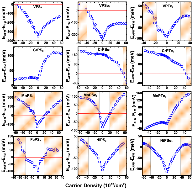
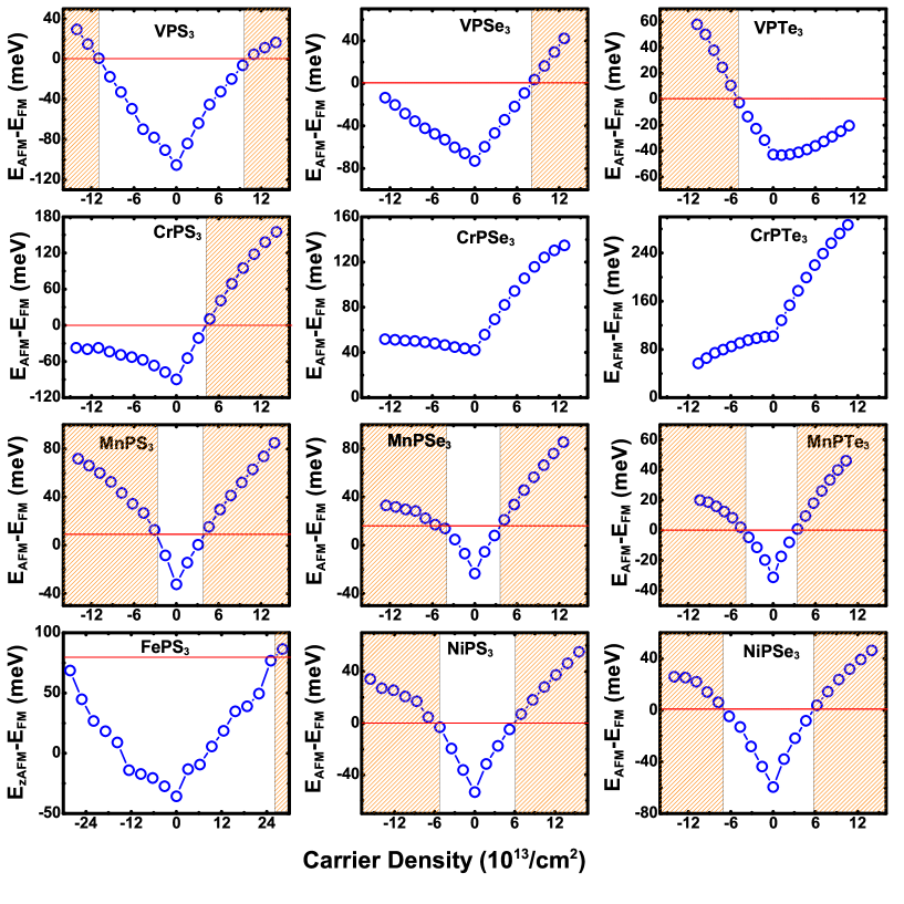
We leave to future work a complete microscopic analysis of the response of a MPX3 layer, acting as one electrode of a capacitor, to a gate voltage. Here we capture the most important response by simply examining the dependence of magnetic properties on carrier density. In doing so we neglect the possible role of charge polarization within a MPX3 layer. Fig. 7 summarizes the theoretically predicted trends in competition between AFM and FM states in 2D MPX3 compounds with M = V, Cr, Mn, Fe, Ni and X = S, Se, Te. We find that when the magnetic ground state is AFM (M= V, Mn, Ni, Fe), transitions to FM states are driven by sufficiently large electron or hole carrier densities. The origin of this trend is easy to understand. Because the FM state is gapless the energy changes associated with adding one electron and removing one electron are identical. In the gapped AFM states they differ by the energy gap . It follows that the energy difference per area unit between antiferromagnetic and ferromagnetic states is given at low carrier densities by
| (5) |
where is the carrier density of -type samples, is the carrier density of -type samples, is the energy difference per area unit between antiferromagnetic and ferromagnetic states in neutral MPX3 sheets, and is the difference between the mid-gap energy of the antiferromagnetic semiconductors and the chemical potential of the ferromagnetic metals. Introducing -carriers is most effective in driving a transition from antiferromagnetic to ferromagnetic states when is positive, whereas introducing -carriers is most effective when is negative. By comparing with Fig. 7 we conclude that is small in most cases, but large and negative in MnPS3 and MnPSe3. Because the energy difference per formula unit between ferro and antiferromagnetic states is much smaller than the energy gap, a transition between antiferromagnetic and ferromagnetic states can be driven by carrier density changes per formula unit that are much smaller than one - especially so when plays a favorable role. In particular we see in Fig. 7 that a transition between ferromagnetic and antiferromagnetic states are predicted in MnPS3 and MnPSe3 at hole carrier densities that are , which corresponds to about 0.16 electrons per formula unit. Density changes of this magnitude can be achieved by ionic liquid or gel gating. Since this size of carrier density is sufficient to completely change the character of the magnetic order, we can expect substantial changes in magnetic energy landscapes at much smaller carrier densities. Transitions between ferromagnetic and antiferromagnetic states are predicted in most MPX3 compounds. Our calculations show that the FM solution is the preferred stable magnetic configuration in almost all cases when the system is subject to large electron or hole densities in the range above a few times cm-2. The DOS and PDOS shown in Figs. 5-6 in the main text and in Figs. 5-10 in the Supplemental Material may suggest that a Stoner ferromagnetic instability is at play when the peaks near the band edges are sufficiently prominent. Our calculations therefore motivate efforts to find materials which can be used to establish good electrical contacts to MPX3 compounds, and in particular to the valence bands of MnPS3 and MnPSe3. For the Cr based compounds, whose behavior is different, the ground states at zero carrier density is FM and we find that a transition to an AFM state can occur for -doped systems.
IV.2 Strain-tunable magnetic properties
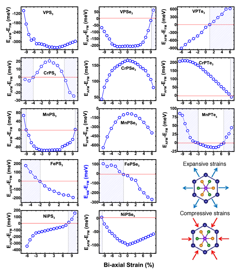
The membrane-like flexibility of ultrathin 2D materials makes them suitable platforms for tailoring the electronic structure properties by means of strains. Representative examples on effects of strains in 2D materials properties that have been discussed in recent literature include the observation of Landau-level like density of states near high curvature graphene bubbles guineabubbles , or the commensuration moire strains that opens up a band gap at the primary Dirac point in graphene on hexagonal boron nitride for sufficiently long moire patterns jarillogap ; woods ; origingap . The sensitive variation of the different M-M, P-P, M-X bond lengths as a function of magnetic configuration we have presented earlier in Sec. III suggests that strains can be used as switches to trigger magnetic phase transitions or alter the stability of the magnetic phases by modifying the total energy difference with respect to the non-magnetic phases. Here we have carried out calculations of the total energies for different magnetic phases to explore the influence of expansive or compressive in-plane biaxial and uniaxial strains and the effects of external pressure along the out-of plane axis in 2D MPX3 materials. The compressive and expansive biaxial strains have been modeled through uniform scaling of the rectangular unit cell in Fig. 1 and likewise the uniaxial strains are modeled by scaling the unit cell either in the zigzag or armchair directions. We notice that generally the effects of uniform biaxial versus uniaxial strains introduce modifications in the magnetic phase energy difference total energies that are qualitatively similar for the compressive or expansive strains, and that the effects are stronger for biaxial strains when compared to uniaxial strains which do not show a noticeable difference between the zigzag or armchair directions. Pressure strains along the out of plane vertical c-axis have been applied by artificially modifying the P-P distance and we find for MnPS3 a clear transition from AFM to FM with the total energy difference changing from 93 meV to 268 meV per formula unit in the presence of a 4% bond length shortening strain for the P-P distance. Relatively large strains are required to alter the magnetic properties in compounds like MnPS3 but other systems such as CrPS3, FeP, FePSe3 NiPS3 and VPTe3 the magnetic phase transitions can be achieved for smaller strains as they have relatively smaller total energy differences between the magnetic phases. We find a particularly sensitive transition near charge neutrality for FePS3, FePSe3 and VPTe3 where strains on the order of 1% is enough to switch between different magnetic configurations.
V Summary and discussion
In this paper we have carried out an ab initio study of the MPX3 transition metal phosphorous trichalcogenide class of two-dimensional materials. We have considered different combinations of 3d metals (M = V, Cr, Mn, Fe, Co, Ni, Cu, Zn) and chalcogens (X = S, Se, Te) in an effort to identify materials that are promising for spintronics based on two-dimensional materials. Our calculations suggest that magnetic phases are common in the single-layer limit of these van der Waals materials, and that the configuration of the magnetic state depends systematically on the transition metal/ chalcogen element combination. We find that semiconducting Néel antiferromagnetic states are most common; and predict AFM phases for V, Mn, Fe, and Ni based compounds. A metallic ferromagnetic states is found in Cr based compounds, and non-magnetic states are found with both semiconducting and metallic electronic structure, while introduction of U tends to stabilize the AFM magnetic phase. As expected on the basis of the weaker covalent bonds of larger atomic orbitals we find that for semiconducting antiferromagnetic materials, replacing a smaller chalcogen atom with larger chalcogen atom reduces the energy band gap and as a consequence also the difference between the ground state energies of FM and AFM states. Interestingly we do not find magnetic states for CoPX3, even though Co is typically a magnetic atom.
The electronic structures predicted by density functional theory for these materials are sensitive to the choice of exchange-correlation energy functional. For example, there are substantial discrepancies in predicted densities-of-states between the standard semi-local GGA, approximations with a local U correction, and hybrid functionals with non-local exchange. This sensitivity of the optimized ground-state results to the choice of the approximation scheme makes it desirable to benchmark the results against experiment in order to establish which approximation is most reliably predictive. The fact that the predictions of density-functional theory are qualitatively sensitive to the exchange-correlation approximation employed, indicates that the MPX3 compounds are correlated.
An interesting interdependence between magnetic order and atomic structure was found, with typical variations on the order of a few percents in the lattice constant and interatomic bond lengths leading to structural distortions depending on the magnetic configuration of the system. The bond length variations were traced through M-M, P-P, P-X bond distances associated with the distortions in the honeycomb array of the transition metal atoms and the distance between the atomic centers in the (P2X6)4- bipyramids. We leave for future work the analysis on the role of spin-orbit coupling effects and optical properties arising from lattice symmetry breaking coupled to the onset of magnetism. Sizeable differences between the GGA and the LDA solutions is suggestive of the delicate balance between the different chemical bonds for configuring the optimized structure of these compounds which in turn are affected by the onset of magnetism. In the antiferromagnetic state, the strength of the exchange interactions is expected to vary inversely with the band gap; approximations that underestimate the band gap will overestimate exchange interaction strengths. We expect that the LDA likely does underestimate band gaps, as it commonly does, and therefore the exchange interactions it implies may well be overestimates. In 2D MPX3 a variety of different stable and meta-stable magnetic configurations were found. Semiconducting states with a band gap are typically antiferromagnetic phases in either Néel, zigzag, or stripy configuration and the metallic states are typically ferromagnetic phases. The critical temperatures for magnetic phases in the single layer limit are generally expected to be smaller than in the bulk due to the reduction in the number of close neighbor exchange interactions, although changes in the degree of itineracy and shifts in relative band positions can also play a role. We analyzed the magnetic phases of the 2D MPX3 compounds by building an effective model Hamiltonian with exchange coupling parameters extracted by mapping the total energies from our ab initio calculations onto an effective classical spin model. The Curie and Néel temperatures TC, TN are obtained by using a statistical analysis based on the Metropolis algorithm newman . The calculated Néel temperatures of the antiferromagnetic compounds have a wide range of variation, ranging between a few to a few hundred Kelvin.
Control of magnetic phases by varying the electric field in a field effect transistor device is a particularly appealing strategy for 2D magnetic materials. Our calculations indicate that a transition between antiferromagnetic and ferromagnetic phases can be achieved by inducing carrier densities in 2D MPX3 compounds that are in the range that can be induced by a field effect. We find that a magnetic phase transition from a FM state to an AFM state can be induced in metallic CrPSe3 and CrPTe3 compounds, which are close to the phase boundary, by gating to large n-type carrier densities. Similarly AFM to FM transitions can be achieved in VPTe3, MnPTe3, and FePS3. For materials exhibiting magnetic phases we find that using the heavy chalcogen Te can reduce the carrier densities required for magnetic transitions.
The interdependence between atomic and electronic structure suggest that strains can be employed to tune magnetic phases. We have found that the ground state magnetic configuration can undergo phase transitions driven by in-plane compression or expansion of the lattice constants or by as c-axis pressure. The magnitude of the required strains vary greatly, with values below 1% for compounds such as FePS3, FePSe3 and VPTe3, and larger strains on the order of or far greater than 4% are required to trigger a FM-AFM magnetic phase transition in CrPS3 and NiPS3. Phase transitions for even larger strains on the order of 9% are observed in VPSe3, MnPS3, NiPS3, NiPSe3 whose non-strained configuration has a robust gapped antiferromagnetic phase.
Based on our calculations, we conclude that single layer MPX3 transition metal thiophosphates are interesting candidate materials for 2D spintronics. Their properties, including their magnetic transition temperatures, can be adjusted by the application of external strains or by modifying the carrier densities in field effect transistor devices. The sensitivity of these systems to variations in system parameters, such as composition stoichiometry, details of the interface, and the exchange coupling of the magnetic properties with external fields, offers ample room for future research that seek new functionalities.
VI Acknowledgements
We are thankful to the assistance from and computational resources provided by the Texas Advanced Computing Centre (TACC). JJ was supported by the 2015 Research Fund of the University of Seoul. This work was also supported by NRF-2014R1A2A2A01006776 for EHH, DOE BES Award SC0012670, and Welch Foundation grant TBF1473 for AHM, and NRF-2015R1D1A1A01060381 for MH. We acknowledge helpful discussions with J. D. Noh on the calculation of the critical temperatures of the magnetic phases.
References
- (1) K. S. Novoselov, A. K. Geim, S. V. Morozov, D. Jiang, M. I. Katsnelson, I. V. Grigorieva, S. V. Dubonos and, A. A. Firsov, Two-dimensional gas of massless Dirac fermions in graphene, Nature. 438, 197 (2005).
- (2) Y. Zhang, Y.-W. Tan, H. L. Stormer, and P. Kim, Experimental observation of the quantum Hall effect and Berry’s phase in graphene, Nature. 438, 201 (2005).
- (3) K. S. Novoselov, D. Jiang, F. Schedin, T. J. Booth, V. V. Khotkevich, S. V. Morozov, and A. K. Geim, Two-dimensional atomic crystals, Proc. Nat. Ac. Sci. 102, 10451 (2004).
- (4) M. Chhowalla, H. S. Shin, G. Eda, L-J. Li, K. P. Loh and, H. Zhang, The chemistry of two-dimensional layered transition metal dichalcogenide nanosheets, Nat. Chem. 5, 263 (2013).
- (5) L. Britnell, R. M. Ribeiro, A. Eckmann , R. Jalil, B. D. Belle, A. Mishchenko, Y. J. Kim, R. V. Gorbachev, T. Georgiou, S. V. Morozov, A. N. Grigorenko, A. K. Geim, C. Casiraghi, A. H. Castro Neto, K. S. Novoselov KS, Strong light-matter interactions in heterostructures of atomically thin films, Science. 340, 1311 (2013).
- (6) B. Burk, R. E. Thomson, J. Clarke, A. Zettl, Surface and Bulk Charge Density Wave Structure in 1 T-TaS2, Science. 257, 362 (1992).
- (7) A. H. Castro Neto, Charge Density Wave, Superconductivity, and Anomalous Metallic Behavior in 2D Transition Metal Dichalcogenides, Phys. Rev. Lett. 86, 4382 (2001).
- (8) R. F. Frindt, Superconductivity in ultrathin NbSe2 layers, Phys. Rev. Lett. 28, 299 (1972).
- (9) D. Costanzo, S. Jo, H. Berger, and A. F. Morpurgo, Gate-induced superconductivity in atomically thin MoS2 crystals, Nat. Nanotech. 11, 339 (2016).
- (10) Magnetic Properties of Layered Transition Metal Compounds Ed by L. J. de Jongh, series of Physics and Chemistry of Materials with Low-Dimensional Structures, vol- 9 (1990).
- (11) Y. Ma, Y. Dai, M. Guo, C. Niu, Y. Zhu, and B. Huang, Evidence of the Existence of Magnetism in Pristine VX2 Monolayers (X = S, Se) and Their Strain-Induced Tunable Magnetic Properties, ACS Nano, 6, 1695 (2012).
- (12) S. Lebegue, T. Björkman, M. Klintenberg, R. M. Nieminen, and O. Eriksson, Two-Dimensional Materials from Data Filtering and Ab Initio Calculations, Phys. Rev. X 3, 031002 (2013).
- (13) B. Siberchicot, S. Jobic , V. Carteaux , P. Gressier , and G. Ouvrard, Band Structure Calculations of Ferromagnetic Chromium Tellurides CrSiTe3 and CrGeTe3, J. Phys. Chem. 100, 5863, (1996).
- (14) M.-W. Lin, H. L. Zhuang, J. Yan, T. Z. Ward, A. A. Puretzky, C. M. Rouleau, Z. Gai, L. Liang, V. Meunier, B. G. Sumpter, P. Ganesh, P. R. C. Kent, D. B. Geohegan, D. G. Mandrus and K. Xiao, Ultrathin nanosheets of CrSiTe3: a semiconducting two-dimensional ferromagnetic material J. Mater. Chem. C, 4, 315 (2016).
- (15) T. J. Williams, A. A. Aczel, M. D. Lumsden, S. E. Nagler, M. B. Stone, J.-Q. Yan, D. Mandrus, Magnetic Correlations in the Quasi-2D Semiconducting Ferromagnet CrSiTe3, Phys. Rev. B. 92, 144404 (2015).
- (16) X. Chen, J. Qi, and D. Shi, Strain-engineering of magnetic coupling in two-dimensional magnetic semiconductor CrSiTe3: Competition of direct exchange interaction and superexchange interaction, Phys. Lett. A. 379, 60 (2015).
- (17) L. D. Casto, A. J. Clune, M. O. Yokosuk, J. L. Musfeldt, T. J. Williams, H. L. Zhuang, M.-W. Lin, K. Xiao, R. G. Hennig, B. C. Sales, J.-Q. Yan, and D. Mandrus, Strong spin-lattice coupling in CrSiTe3, APL Mater. 3, 041515 (2015).
- (18) N. Sivadas, M. W. Daniels, R. H. Swendsen, S. Okamoto, and D. Xiao, Magnetic ground state of semiconducting transition-metal trichalcogenide monolayers, Phys. Rev. B. 91, 235425 (2015).
- (19) H. L. Zhuang, Y. Xie, P. R. C. Kent, and P. Ganesh, Computational discovery of ferromagnetic semiconducting single-layer CrSnTe3, Phys. Rev. B. 92, 035407 (2015).
- (20) M. A. McGuire, H. Dixit, V. R. Cooper, and B. C. Sales, Coupling of Crystal Structure and Magnetism in the Layered, Ferromagnetic Insulator CrI3, Chem. Mater. 27, 612 (2015).
- (21) W. B. Zhang, Q. Qu, P. Zhu, C. H. Lam, Robust intrinsic ferromagnetism and half semiconductivity in stable two-dimensional single-layer chromium trihalides, J. Mater. Chem. C, 3, 12457 (2015).
- (22) X. Li, X. Wu, and J. Yang, Half-Metallicity in MnPSe3 Exfoliated Nanosheet with Carrier Doping, J. Am. Chem. Soc. 136, 11065 (2014).
- (23) X. Li, T. Cao, Q. Niu, J. Shi, and J. Feng, Coupling the valley degree of freedom to antiferromagnetic order, Proc. Nat. Ac. Sci. 110, 3738 (2013).
- (24) R. Brec, Review on structural and chemical properties of transition metal phosphorous trisulfides MPS3, Solid State Ionics 22, 3, (1986).
- (25) A R Wildes, B Roessli, B Lebech and K W Godfrey, Spin waves and the critical behaviour of the magnetization in MnPS3, J. Phys.: Condens. Matter 10, 6417 (1998).
- (26) E. Prouzet, G. Ouvrard and R. Brec, Structure determination of ZnPS3, Mat. Res. Bull., 21, 195, (1986).
- (27) G. Ouvrard, R. Brec and J. Rouxel, Structural determination of some MPS3 layered phases (M = Mn, Fe, Co, Ni and Cd), Mat. Res. Bull., 20, 1181, (1985).
- (28) G. Ouvrard, R. Freour, R. Brec and J. Rouxel, A mixed valence compound in the two dimensional MPS3 family: V0.78PS3 structure and physical properties, Mat. Res. Bull., 20, 1053, (1985).
- (29) P. A. Joy and S. Vasudevan, Infrared(700-100 cm-1) vibrational spectra of the layered transition metal thiophosphates, MPS3, (M = Mn, Fe AND Ni), J. Phys. Chem. Solids. 54, 343, (1993).
- (30) K. C. Rule, Magnetic ordering in the two dimensional antiferromagnet FePS3, Doctoral Thesis, School of Physics and Material Engineering, Monash University, Australia, (2004).
- (31) E. Ressouche, M. Loire, V. Simonet, R. Ballou, A. Stunault, and A. Wildes Magnetoelectric MnPS3 as a candidate for ferrotoroidicity, Phys. Rev. B. 82, 100408 (2010).
- (32) K. Kurosawa, S. Saito, and Y. Yamaguchi, Neutron Diffraction Study on MnPS3 and FePS3, J. Phys. Soc. Jpn. 52, 3919 (1983).
- (33) W. Klingen, G. Eulenberger, and H. Hahn, About Hexathio- and Hexaselenohypodiphosphate type M2P2X6, The Nature of Science. 55, 229 (1968).
- (34) N. Kurita and K. Nakao, Band structure of magnetic layered semiconductor NiPS3, J. Phys. Soc. Jpn. 58, 232 (1989).
- (35) K. C. Rule, G. J. McIntyre, S. J. Kennedy, and T. J. Hicks, Single-crystal and powder neutron diffraction experiments on FePS3: Search for the magnetic structure Phys. Rev. B. 76, 134402, (2007).
- (36) N. Kurita and K. Nakao, Band Structures and Physical Properties of Magnetic Layered Semiconductors MPS3, J. Phys. Soc. Jpn. 58, 610 (1989).
- (37) G. Le Flem, R. Brec, G. Ouvard, and A. Louisy, P. Segransan, Magnetic interactions in the layer compunds MPX3 (M=Mn,Fe,Ni;X=S,Se) J. Phys. Chem. Solids. 43, 455, (1982).
- (38) D. J. Goossens, Dipolar anisotropy in quasi-2D honeycomb antiferromagnet MnPS3, Eur. Phys. J. B 78, 305 (2010).
- (39) N. Chandrasekharan and S. Vasudevan, Magnetism, exchange and crystal field parameters in the orbitally unquenchedlsing antiferromagnet FePS3, Pramana: J. Phys., 43, 21, (1994).
- (40) P. Jeevanandam and S. Vasudevan, Magnetism in MnPSe3: a layered 3d5 antiferromagnet with unusually large XY anisotropy, J. Phys.: Condens. Matter. 11, 3563 (1999).
- (41) P. A. Joy and S. Vasudevan, Magnetism in the layered transition-metal thiophosphates MPS3 (M =Mn, Fe, and Ni), Phys. Rev. B. 46, 5425 (1992).
- (42) A. R. Wildes, K. C. Rule, R. I. Bewley, M. Enderle and T. J. Hicks, The magnon dynamics and spin exchange parameters of FePS3, J. Phys.: Condens. Matter 24, 416004 (2012).
- (43) A. R. Wildes. S. J. Kennedy and T. J. Hicks, True two-dimensionalmagnetic ordering in MnPS3, J. Phys.: Condens. Matter 6, 335 (1994).
- (44) J. Liu, X.-B. Li, D. Wang, W.-M. Lau, P. Peng, and L.-M. Liu, Diverse and tunable electronic structures of single-layer metal phosphorus trichalcogenides for photocatalytic water splitting, J. Chem. Phys. 140, 054707 (2014).
- (45) C.-T. Kuo, M. Neumann, K. Balamurugan, H. J. Park, S. Kang, H. W. Shiu, J. H. Kang, B. H. Hong, M. Han, T. W. Noh and J.-G. Park, Exfoliation and Raman Spectroscopic Fingerprint of Few-Layer NiPS3 Van der Waals Crystals, Sci. Rep. 6, 20904 (2016).
- (46) C.-T. Kuo, K. Balamurugan, H. W. Shiu, H. J. Park, S. Sinn, M. Neumann, M. Han, Y. J. Chang, C.-H. Chen, H.-D. Kim, J.-G. Park, and T. W. Noh, The energy band alignment at the interface between mechanically exfoliated few-layer NiPS3 nanosheets and ZnO, Curr. Appl. Phys. 16 404-408 (2016).
- (47) J.-U. Lee, S. Lee, J. H. Ryoo, S. Kang, T. Y. Kim, P. Kim, C.-H. Park, J.-G. Park, and H. Cheong, Ising-Type Magnetic Ordering in Atomically Thin FePS3, arXiv:1608.04169 (2016).
- (48) K. Z. Du, X.Z. Wang, Y. Liu, P. Hu, M. I. B. Utama, C. K. Gan, Q. H. Xiong, and C. Kloc, Weak Van der Waals Stacking, Wide-Range Band Gap, and Raman Study on Ultrathin Layers of Metal Phosphorus Trichalcogenides, ACS. Nano. 10, 1738 (2016).
- (49) A. R. Wildes, V. Simonet, E. Ressouche, G. J. McIntyre, M. Avdeev, E. Suard, S. A. J. Kimber, D. Lançon, G. Pepe, B. Moubaraki, and T. J. Hicks, Magnetic structure of the quasi-two-dimensional antiferromagnet NiPS3, Phys. Rev. B. 92, 224408 (2015).
- (50) R. Brec, D.M. Schleigh, G. Ouvrard, A. Louisy, and J. Rouxel, Physical Properties of Lithium Intercalation Compounds of the Layered Transition Chalcogenophosphates, Inorg. Chem. 18, 1814 (1979).
- (51) P. J. S. Foot, T. Katz, S. N. Patel, B. A. Nevett, A. R. Piercy, and A. A. Balchin, The structures and conduction mechanisms of lithium-intercalated and lithium-substituted nickel phosphorus trisulphide (NiPS3), and the use of the material as a secondary battery electrode, Phys. Stat. Soi. A. 100, 11 (1987).
- (52) P. J. S. Foot and B. A. Nevett, Electronic Conduction in p- and n-Type NiPS3, Phys. Stat. Sol. A. 93, 283 (1986).
- (53) R. Clement, Ion-Exchange Intercalation into the MPS3 Layered Compounds Hybrid Organic-Inorganic Composites, ACS. Symp. Ser. 585, 29 (1995).
- (54) Y. Mathey, R. Clement, J. P. Audiere, O. Poizat, and C. Sourisseau, Structural, vibrational and conduction properties of a new class of layer-type MPS3 compounds, Mn MPS3 (MI = Cu, Ag), Solid. State. Ionics 9 10, 459 (1983).
- (55) P. Giannozzi, S. Baroni, N. Bonini, M. Calandra, R. Car, C. Cavazzoni, D. Ceresoli, G. L. Chiarotti, M. Cococcioni, I. Dabo, A. D. Corso, S. de Gironcoli, S. Fabris, G. Fratesi, R. Gebauer, U. Gerstmann, C. Gougoussis, A. Kokalj, M. Lazzeri, L. Martin-Samos, N. Marzari, F. Mauri, R. Mazzarello, S. Paolini, A. Pasquarello, L. Paulatto, C. Sbraccia, S. Scandolo, G. Sclauzero, A. P. Seitsonen, A. Smogunov, P. Umari, and R. M. Wentzcovitch, QUANTUM ESPRESSO: a modular and open-source software project for quantum simulations of materials, J. Phys.: Cond. Matter. 21, 395502 (2009).
- (56) J. P. Perdew, K. Burke, and M. Ernzerhof, Generalized Gradient Approximation Made Simple, Phys. Rev. Lett. 77, 3865 (1996).
- (57) S. Grimme, Semiempirical GGA-type density functional constructed with a long-range dispersion correction, J. Comp. Chem. 27, 1787 (2006).
- (58) J. P. Perdew and A. Zunger, Self-interaction correction to density-functional approximations for many-electron systems, Phys. Rev. B. 23, 5048 (1981).
- (59) N. Marom, J. Bernstein, J Garel, A. Tkatchenko, E. Joselevich, L. Kronik, and O. Hod, Stacking and Registry Effects in Layered Materials: The Case of Hexagonal Boron Nitride, Phys. Rev. Lett. 105, 046801 (2010).
- (60) J. Heyd, G. Scuseria, and M. Ernzerhof, Hybrid functionals based on a screened Coulomb potential, J. Chem. Phys. 118, 8207 (2003).
- (61) See Supplemental Material at http://link.aps.org/supplemental/ for the lattice structures, band structures, the associated density of states and the orbital projected density of states (PDOS) calculated for self-consistently converged magnetic configurations with total energy local minima with the energy origin E=0 is placed at the valence band edge for gapped bands. Carrier density dependent magnetic phase transition is calculated using a finite onsite repulsion U=4 eV on the of GGA+D2. We also obtain the magnetization as a function of temperature through the Metropolis Monte Carlo simulation in a 3264 superlattice.
- (62) J. Chaloupka, G. Jackeli, and G. Khaliullin, Zigzag Magnetic Order in the Iridium Oxide Na2IrO3, Phys. Rev. Lett. 110, 097204 (2013).
- (63) N. Metropolis, A. W. Rosenbluth, M. N. Rosenbluth, A. H. Teller, E. Teller, Equation of State Calculations by Fast Computing Machines J. Chem. Phys. 21, 1087 (1953).
- (64) M. E. J. Newman and G. T. Barkema, Monte Carlo Methods in Statistical Physics, Clarendon Press, Oxford (1999).
- (65) D. P. Landauand K. Binder, Monte Carlo Simulations in Statistical Physics, Cambridge University Press, Cambridge (2000)/
- (66) D. P. Landau, S.-H. Tsai, and M. Exler, A new approach to Monte Carlo simulations in statistical physics: Wang-Landau sampling, Am. J. Phys. 72, 10 (2004).
- (67) F. Matsukura, Y. Tokura, and Hideo Ohno, Control of magnetism by electric fields, Nat. Nanotech. 10, 209 (2015).
- (68) H. Ohno, D. Chiba, F. Matsukura, T. Omiya, E. Abe, T. Dietl, Y. Ohno, and K. Ohtani, Electric-field control of ferromagnetism, Nature. 408, 944 (2000).
- (69) M. Endo, S. Kanai, S. Ikeda, F. Matsukura and H. Ohno, Electric-field effects on thickness dependent magnetic anisotropy of sputtered MgO/Co40Fe40B20/Ta structures, App. Phys. Lett. 96, 212503 (2010).
- (70) N. Levy, S. A. Burke, K. L. Meaker, M. Panlasigui, A. Zettl, F. Guinea, A. H. Castro Neto, M. F. Crommie, Strain-Induced Pseudo-Magnetic Fields Greater Than 300 Tesla in Graphene Nanobubbles, Science. 329, 544 (2010).
- (71) B. Hunt, J. D. Sanchez-Yamagishi, A. F. Young, M. Yankowitz, B. J. LeRoy, K. Watanabe, T. Taniguchi, P. Moon, M. Koshino, P. Jarillo-Herrero, and R. C. Ashoori, Massive Dirac Fermions and Hofstadter Butterfly in a van der Waals Heterostructure, Science. 340, 1427 (2013).
- (72) C. R. Woods, L. Britnell, A. Eckmann, R. S. Ma, J. C. Lu, H. M. Guo, X. Lin, G. L. Yu, Y. Cao, R. V. Gorbachev, A. V. Kretinin, J. Park, L. A. Ponomarenko, M. I. Katsnelson, Yu. N. Gornostyrev, K. Watanabe, T. Taniguchi, C. Casiraghi, H-J. Gao, A. K. Geim and K. S. Novoselov, Commensurate-incommensurate transition in graphene on hexagonal boron nitride, Nat. Phys. 10, 451 (2014).
- (73) J. Jung, A. M. DaSilva, A. H. MacDonald, and Shaffique Adam, Origin of band gaps in graphene on hexagonal boron nitride, Nat. Commun. 6 6308 (2015).
Supplementary Information
We present the lattice structures, band structures, the associated density of states and the orbital projected density of states (PDOS) calculated for self-consistently converged magnetic configurations with total energy local minima with the energy origin E=0 is placed at the valence band edge for gapped bands. Carrier density dependent magnetic phase transition is calculated using a finite onsite repulsion U=4 eV on the of GGA+D2. We also obtain the magnetization as a function of temperature through the Metropolis Monte Carlo simulation in a 3264 superlattice.
| MPX3 | LDA | GGA | |||||||||||
|---|---|---|---|---|---|---|---|---|---|---|---|---|---|
| FM | AFM | NM | FM | AFM | NM | ||||||||
| X | a(Å) | c′(Å) | a(Å) | c′(Å) | a(Å) | c′(Å) | a(Å) | c′(Å) | a(Å) | c′(Å) | a(Å) | c′(Å) | |
| S | 5.616 | 3.106 | 5.675 | 3.109 | 5.616 | 3.106 | 5.913 | 3.061 | 5.886 | 3.161 | 5.7647 | 3.134 | |
| VPX3 | Se | 5.951 | 3.230 | 6.053 | 3.245 | 6.001 | 3.221 | 6.249 | 3.234 | 6.259 | 3.313 | 6.167 | 3.251 |
| Te | 6.452 | 3.595 | 6.608 | 3.418 | 6.459 | 3.449 | 6.409 | 3.680 | 7.087 | 3.417 | 6.963 | 3.294 | |
| S | 5.716 | 2.922 | 5.771 | 3.004 | 5.745 | 3.028 | 5.957 | 3.016 | 5.928 | 3.337 | 5.886 | 3.061 | |
| CrPX3 | Se | 6.186 | 3.018 | 6.170 | 3.111 | 6.181 | 3.147 | 6.368 | 3.077 | 6.322 | 3.140 | 6.354 | 3.179 |
| Te | 6.654 | 3.285 | 6.646 | 3.291 | 6.664 | 2.926 | 6.862 | 3.358 | 6.881 | 3.359 | 6.551 | 3.046 | |
| S | 5.667 | 2.865 | 5.869 | 3.138 | 5.691 | 2.877 | 6.086 | 3.246 | 6.058 | 3.235 | 5.814 | 2.932 | |
| MnPX3 | Se | 6.0916 | 2.925 | 6.198 | 3.271 | 6.125 | 2.964 | 6.409 | 3.417 | 6.395 | 4.017 | 6.090 | 2.966 |
| Te | 6.602 | 3.123 | 6.712 | 3.041 | 6.625 | 3.014 | 6.841 | 3.565 | 6.951 | 3.533 | 6.554 | 3.215 | |
| S | 5.639 | 2.702 | 5.639 | 2.702 | 5.638 | 2.702 | 5.914 | 3.072 | 5.963 | 3.105 | 5.758 | 2.786 | |
| FePX3 | Se | 6.035 | 2.800 | 6.036 | 2.800 | 6.035 | 2.800 | 6.290 | 3.294 | 6.326 | 3.205 | 6.180 | 2.876 |
| Te | 6.545 | 2.957 | 6.740 | 2.998 | |||||||||
| S | 5.677 | 2.682 | 5.801 | 2.7571 | |||||||||
| CoPX3 | Se | 6.093 | 2.764 | 6.241 | 2.175 | ||||||||
| Te | 6.572 | 2.986 | 6.763 | 3.027 | |||||||||
| S | 5.662 | 2.880 | 5.655 | 2.876 | 5.655 | 2.876 | 5.824 | 3.059 | 5.8147 | 3.036 | 5.795 | 2.963 | |
| NiPX3 | Se | 6.020 | 2.978 | 6.020 | 2.988 | 6.020 | 2.978 | 6.181 | 3.073 | 6.181 | 3.124 | 6.177 | 3.060 |
| Te | 6.553 | 3.099 | 6.898 | 3.030 | |||||||||
| S | 5.711 | 3.313 | 5.900 | 3.474 | |||||||||
| CuPX3 | Se | 6.043 | 3.278 | 6.222 | 3.186 | ||||||||
| Te | 6.496 | 3.511 | 6.770 | 3.347 | |||||||||
| S | 5.826 | 3.174 | 6.022 | 3.224 | |||||||||
| ZnPX3 | Se | 6.170 | 3.314 | 6.382 | 3.385 | ||||||||
| Te | 6.672 | 3.533 | 6.898 | 3.599 | |||||||||
| MPX3 | X | M-M | P-P | P-X | ||||||
|---|---|---|---|---|---|---|---|---|---|---|
| NM | FM | AFM | NM | FM | AFM | NM | FM | AFM | ||
| S | 3.313, 3.311 | 3.500, 3.230 | 3.377, 3.372 | 2.193 | 2.181 | 2.185 | 2.050 | 2.070, 2.087 | 2.055 | |
| VPX3 | Se | 3.535 | 3.743, 3.375 | 3.587 | 2.208 | 2.199 | 2.203 | 2.235 | 2.284, 2.254 | 2.236 |
| Te | 3.976, 3.974 | 4.002, 4.005 | 4.030, 4.028 | 2.182 | 2.198 | 2.205 | 2.526 | 2.507 | 2.518 | |
| S | 3.060, 3.836 | 3.414 | 3.363, 3.558 | 2.167 | 2.214 | 2.208 | 2.093, 2.029 | 2.078 | 2.080, 2.031 | |
| CrPX3 | Se | 4.115, 2.650 | 3.648 | 3.700, 3.510 | 2.174 | 2.245 | 2.243 | 2.264, 2.667 | 2.334 | 2.325, 2.292 |
| Te | 4.426, 2.868 | 3.971,3.970 | 3.930, 3.928 | 2.163 | 2.228 | 2.231 | 2.501, 2.793 | 2.598, 2.596 | 2.578, 2.580 | |
| S | 3.199, 3.539 | 3.477 | 3.463, 3.462 | 2.152 | 2.212 | 2.211 | 2.092, 2.068 | 2.041 | 2.038 | |
| MnPX3 | Se | 3.983, 2.883 | 3.660 | 3.657, 3.655 | 2.171 | 2.234 | 2.232 | 2.267, 2.687 | 2.217 | 2.213 |
| Te | 4.236, 3.162 | 3.929 | 3.969, 3.967 | 2.160 | 2.239 | 2.240 | 2.505, 2.762 | 2.487 | 2.470 | |
| S | 3.307 | 3.403, 3.397 | 3.463, 3.608 | 2.140 | 2.194 | 2.198 | 2.106 | 2.042 | 2.054, 2.047 | |
| FePX3 | Se | 3.540 | 3.705, 3.415 | 3.623, 3.624 | 2.158 | 2.216 | 2.206 | 2.304 | 2.220, 2.230 | 2.236 |
| Te | 3.853, 3.855 | 2.16 | 2.566 | |||||||
| S | 3.327 | 2.224 | 2.098 | |||||||
| CoPX3 | Se | 3.571 | 2.254 | 2.360 | ||||||
| Te | 3.863, 3.916 | 2.217 | 2.590, 2.683 | |||||||
| S | 3.329 | 3.344 | 3.339 | 2.199 | 2.174 | 2.184 | 2.399 | 2.052 | 2.043 | |
| NiPX3 | Se | 3.540 | 3.541 | 3.544,3.543 | 2.234 | 2.236 | 2.217 | 2.227 | 2.235 | 2.224 |
| Te | 3.848, 3.876 | 2.249 | 2.521, 2.536 | |||||||
| S | 3.425, 3.499 | 2.215 | 2.012, 2.084 | |||||||
| CuPX3 | Se | 3.574, 3.708 | 2.237 | 2.188, 2.248 | ||||||
| Te | 3.925, 3.709 | 2.243 | 2.457, 2.462 | |||||||
| S | 3.445, 3.443 | 2.209 | 2.040 | |||||||
| ZnPX3 | Se | 3.652, 3.641 | 2.232 | 2.214, 2.213 | ||||||
| Te | 3.946, 4.038 | 2.253 | 2.458, 2.462 |
| MPX3 | X | GGA (Triangular) | LDA (Triangular) | ||||
|---|---|---|---|---|---|---|---|
| NM | FM | AFM | NM | FM | AFM | ||
| S | 1133.2 | 665.4 | 0.0 | 263.8 | 276.8 | 0.0 | |
| VPX3 | Se | 1389.1 | 405.6 | 0.0 | 503.7 | 155.1 | 0.0 |
| Te | 1237.6 | 1030.0 | 0.0 | 275.3 | 724.3 | 0.0 | |
| S | 1220.2 | 0.0 | 41.78 | 275.7 | 0.0 | 251.3 | |
| CrPX3 | Se | 1737.4 | 0.0 | 331.7 | 737.5 | 0.0 | 328.6 |
| Te | 1479.4 | 0.0 | 286.2 | 881.0 | 0.0 | 276.9 | |
| S | 2104.9 | 186.9 | 0.0 | 439.7 | 0.0 | 352.2 | |
| MnPX3 | Se | 1351.9 | 157.7 | 0.0 | 510.6 | 0.0 | 274.0 |
| Te | 792.9 | 17.35 | 0.0 | 430.8 | 0.0 | 66.08 | |
| S | 141.1 | 0.0 | 329.7 | 0.0 | |||
| FePX3 | Se | 0.0 | 162.2 | 312.2 | 0.0 | ||
| Te | 0.0 | 0.0 | |||||
| S | 0.0 | 0.0 | |||||
| CoPX3 | Se | 0.0 | 0.0 | ||||
| Te | 0.0 | 0.0 | |||||
| S | 435.8 | 207.48 | 0.0 | 79.55 | 44.89 | 0.0 | |
| NiPX3 | Se | 166.5 | 152.5 | 0.0 | 0.0 | ||
| Te | 0.0 | 0.0 | |||||
| S | 0.0 | 0.0 | |||||
| CuPX3 | Se | 0.0 | 0.0 | ||||
| Te | 0.0 | 0.0 | |||||
| S | 0.0 | 0.0 | |||||
| ZnPX3 | Se | 0.0 | 0.0 | ||||
| Te | 0.0 | 0.0 | |||||
| MPX3 | X | Rectangular | Triangular | Work function (eV) | ||||||||
| NM | FM | AFM | zAFM | sAFM | NM | FM | AFM | NM | FM | AFM | ||
| S | 12175 | 423.4 | 0.0 | 251.9 | 130.6 | 210.6 | 213.6 | 0.0 | 1.41 | 2.58 | 3.12 | |
| VPX3 | Se | 10055 | 298.2 | 0.0 | 169.9 | 93.2 | 149.0 | 148.4 | 0.0 | 1.73 | 2.36 | 2.05 |
| Te | 9564 | 183.1 | 0.0 | 648.9 | 48.9 | 4850 | 85.6 | 0.0 | 1.20 | 1.59 | 1.31 | |
| S | 10282 | 163.2 | 0.0 | 188.3 | 8.16 | 5553 | 179.3 | 0.0 | 1.67 | 2.17 | 2.36 | |
| CrPX3 | Se | 10583 | 60.6 | 0.0 | 148.7 | 47.3 | 5587 | 0.0 | 84.1 | 1.67 | 1.90 | 2.04 |
| Te | 10855 | 213.8 | 478.7 | 504.4 | 0.0 | 5877 | 0.0 | 204.2 | 0.91 | 1.23 | 1.49 | |
| S | 12807 | 129.2 | 0.0 | 51.7 | 58.7 | 7013 | 64.6 | 0.0 | 2.05 | 1.53 | 1.77 | |
| MnPX3 | Se | 15744 | 92.5 | 0.0 | 31.2 | 47.2 | 6578 | 46.6 | 0.0 | 1.94 | 1.60 | 1.71 |
| FePX3 | S | 4779 | 183.0 | 0.0 | 28.5 | 100.6 | 2433 | 0.0 | 1327 | 3.01 | 2.67 | 2.71 |
| NiPX3 | S | 2621 | 318.6 | 91.1 | 0.0 | 321.1 | 1292 | 106.6 | 0.0 | 1.99 | 2.26 | 2.00 |
| Se | 2036 | 292.5 | 54.4 | 0.0 | 303.4 | 996.7 | 118.9 | 0.0 | 1.48 | 1.81 | 2.14 | |