Effects of Oxygen Contamination on Monolayer GeSe: A computational study
Abstract
Natural oxidation is a common degradation mechanism of both mechanical and electronic properties for most of the new two-dimensional materials. From another perspective, controlled oxidation is an option to tune material properties, expanding possibilities for real-world applications. Understanding the electronic structure modifications induced by oxidation is highly desirable for new materials like monolayer GeSe, which is a new candidate for near-infrared photodetectors. By means of first-principles calculations, we study the influence of oxygen defects on the structure and electronic properties of the single layer GeSe. Our calculations show that the oxidation is an exothermic process, and it is nucleated in the germanium sites. The oxidation can cause severe local deformations on the monolayer GeSe structure and introduces a deep state in the bandgap or a shallow state near the conduction band edge. Furthermore, the oxidation increases the bandgap by up to 23%, and may induce direct to indirect bandgap transitions. These results suggest that the natural or intentionally induced monolayer GeSe oxidation can be a source of new optoelectronic properties, adding another important building block to the two-dimensional layered materials.
I Introduction
The group IV monochalcogenide (GIVM) semiconductors family, based on germanium (Ge), tin (Sn) and the chalcogenides sulfur (S), sellenium (Se), and tellurium (Te), have promising properties for the development of a new generation of optoelectronic,II et al. (2010); Mukherjee et al. (2013); DimitriD. Vaughn et al. (2012); Xue et al. (2012) photovoltaic,Antunez et al. (2011) and thermoelectricDing et al. (2015) devices. Furthermore, they are earth abundantSurvey (2002) and environmental friendly.Antunez et al. (2011) GIVM are pointed as an alternative for solar cells, as they are less toxic than other compounds used for photovoltaic applications, e.g.: Pb, Cd, Te. They can be synthesized by using cheaper routes like colloidal solutions, and have bandgaps in a suitable range for photovoltaic applications (1.1–1.5 eV).Antunez et al. (2011) Besides, these compounds present interesting properties for the design of new thermoelectric devices, as anisotropic electronic and thermal conductivity.Ding et al. (2015) GeSe is being envisioned for non-volatile memory applications,Kügeler et al. (2011); Bräuhaus et al. (2008) and GeSe nanosheet-based devices have shown promising properties for near-infrared photodetectors.Mukherjee et al. (2013)
The bulk GeSe crystal is a p-type semiconductor, described by an orthorhombic cell with the D space group and an unit cell with eight atoms, and two layers. Each layer has four three-fold coordinated atoms, with polar-covalent Ge–Se bonds, which form zig-zag chains along the minor crystal axis (b [see Fig. 1(a)]). The layers interact with each other by weak van der Waals interactions, and the crystal can be easily cleaved along the crystal axis perpendicular to the layers (c [see Fig. 1(b)]). Indeed, mechanical exfoliation of bulk GeSe has been reported to produce nanosheets of 57 nm thick.Mukherjee et al. (2013) The comparison of the bulk phase electronic dispersion along the in-plane and out-of-plane directions shows the 2D nature of its electronic properties.Taniguchi et al. (1990) Single-crystal nanosheets of GeSe were recently synthesized,II et al. (2010) revealing promising optoelectronic applications with an onset for optical absorption at about 1.075(5) eV Elkorashy (1986); II et al. (2010) and indirect (direct) bandgap estimated to be 1.14 eV (1.21 eV).II et al. (2010) Similar values are reported on photoconductivity measurements at room temperature.Elkorashy (1989)
Usually, the manipulation and use of devices is carried under ambient conditions, and the samples may suffer oxidation depending on its reactivity. GeSe nanobelts were observed to be coated by an 5 nm thick amorphous germanium oxide layer, which is dissolved after a few-minute water immersion.DimitriD. Vaughn et al. (2012) Although this loss of material does not affect the bulk crystal, it may have pronounced impact on few-layer GeSe devices. Germanium oxide is known to form on the surface of Ge-based materials. As an example, Ge nanowires readily oxidize upon air exposure, resulting in low-performance Ge nanowire-based field-effect-transistors.Hanrath et al. (2005) Thus, a better understanding of the oxidation effects on few-layer GeSe is highly desirable to support further developments on GeSe-based nanotechnology.
In this work we show that oxidation of monolayer GeSe is an exothermic process, and it can result on severe local geometry deformations at the oxidation sites. Our calculations indicate that oxidation occurs preferentially at germanium sites through Ge–O bonding. However, more complex defects involving oxygen bonding to both germanium and selenium are not ruled out. The resulting defects can introduce a deep state in the bandgap or a shallow state at the edge of the conducting band. Furthermore, the bandgap of the oxidized structures can increase by up to 23% in comparison to the pristine monolayer, representing a blue-shift of the material absorption edge. In addition, the oxidation can promote a direct to indirect bandgap transition. These changes may be useful for customizing the material electronic properties.
II Methodology
We model the monolayer GeSe oxidation by using first-principles calculations, based on the density functional theory,Hohenberg and Kohn (1964); Kohn and Sham (1965) as implemented in the QUANTUM ESPRESSO package.Giannozzi et al. (2009) The Brillouin zone sampling are performed within Monkhorst-Pack scheme,Monkhorst and Pack (1976) by using and -centered grids for the supercell slab model () and bulk geometry relaxations, respectively, and a -centered grid for the calculations of the electronic structure of the monolayer. We use a vacuum region of 14.0 Å in our slab model. For lattice and atomic position optimizations, convergence is achieved for forces and stresses lower than 0.1mRy/bohr and 50 MPa, respectively. The exchange-correlation energy is evaluated with generalized gradient approximation (GGA), using Perdew-Burke-Ernzerhof parametrization.Perdew et al. (1996) The valence electron-ion interactions are described using projector-augmented wave (PAW)Blöchl (1994) potentials. The plane-waves kinetic energy cutoff to describe the electronic wave functions (charge density) is set to 50 Ry (400 Ry). To avoid spin contamination in the O2 gas ground-state calculations, we perform spin polarized calculations, imposing the triplet configuration for the O2 molecule.Jhi et al. (2000); Chan et al. (2003)
III Results and Discussion
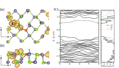
In Fig. 1(a) and (b) we show the pristine monolayer GeSe geometry and the electron localization function (ELF)Savin et al. (1997) plot (isovalue 0.92). Some of the germanium and selenium sites are labeled to further reference. As an example, the Ge(1) refers to the germanium at site (1) and Se(1) refers to the selenium at site (1), just below Ge(1). The ELF plot shows the Ge lone pairs, which are expected to be highly reactive. An ELF contour map along the Ge–Se bond (not shown) reveals its polar-covalent bond nature.
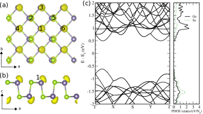
The relaxed lattice parameters are Å and Å, the crystal belongs to the C space group. In comparison to the relaxed bulk GeSe lattice parameters, contracts by % and expands by %. Our calculated bulk lattice parameters values differ by % and % for and , respectively, from the experimental values reported in Ref. Wiedemeier and von Schnering, 1978, and by % and % for and , respectively, from the experimental values reported in Ref. II et al., 2010. The monolayer lattice parameter modifications with respect to bulk values have also been observed on recent theoretical works.Gomes and Carvalho (2015) We observed the stretching of the Ge–Se bonds in the zig-zag direction by 2.3%. The Ge–Se bonds along the –direction decreases by 2.0% and the height difference between the Ge and Se atoms at the zig-zag chain is 0.11 Å in the monolayer, representing a decrease of 57% in comparison to the bulk value (0.26 Å). We calculate a direct bandgap of 1.11 eV, along the –direction on its Brillouin Zone [Fig. 1(c) left] in agreement with calculations using similar methods.Gomes and Carvalho (2015) This value should be considered a lower bound for the experimental bandgap, which is unknown to our knowledge. From the projected density of states (PDOS) we see that the germanium states give the major contribution to the conducting bands [see Fig. 1(c) right].
Interstitial oxygen can occupy several sites on monolayer GeSe and here we considered some of the high symmetry sites, as explained as follows. The oxygen is placed on top of Ge (top–Ge), on top of Se (top–Se), on the interstitial site along the Ge(1)–Se(1) bond [see Fig. 1(b)], on the diagonal bridge site connecting two adjacent zig-zag chains through a Ge(1)–O–Se(5) bond, and connecting two adjacent atoms of same atomic specie on the same zig-zag chain, through Ge–O–Ge and Se–O–Se bonds.
To quantify which of these configurations are favorable, we adopt the following definition for chemisorption energy, per oxygen atom:Ziletti et al. (2015)
| (1) |
where , and are the total energies of the oxidized monolayer GeSe, the pristine monolayer GeSe and the O2 triplet molecule, respectively. This definition results in negative for exothermic process and positive otherwise. The binding energies per oxygen atom of the relaxed structures are summarized on Table 1.
| Configurations | (eV) | |
|---|---|---|
| Initial | Final | |
| top–Ge | top–Ge | -0.780 |
| Ge(1)–O–Se(5) | ||
| top–Se | Ge2OSe bridge | -0.410 |
| Se–O–Se | not shown | 0.611 |
| interstitial Ge(1)-Se(1) | bottom–zig-zag (b-zz) | -0.125 |
| Ge–O–Ge | Ge2OGe bridge | -0.994 |
In general, the monolayer GeSe oxidation leads to minor changes on the lattice parameters. The major changes are on stretching, compression and breaking of Ge–Se bonds nearby the oxidation sites, which results in an defect state within the bandgap. We did not find magnetism induced by the oxygen defects in our calculations.
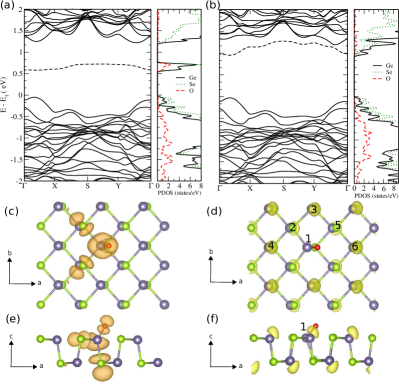
In the simulations with the oxygen starting on the diagonal bridge Ge(1)–Se(5), the Se(5)–O bond breaks remaining only the Ge–O bond, by using the electrons from the Ge(1) lone pair. In the resulting relaxed structure (top–Ge), shown in Fig. 2(d) and (f), the Ge(1) has a tetrahedral-like coordination, resembling that of germanium atoms in bulk phase, and this coordination is expected to be energetically favorable. In comparison to pristine monolayer GeSe, the Ge(1)–Se(2) bond contracts by 6.0%, the Se(2)–Ge(3) bond expands by 3.0%, the Ge(1)–Se(5) distance increases by 13.1%, the Ge(1)–Ge(4) distance decreases by 7.2%, the Ge(1)–Ge(6) distance increases by 10.0%, and the Ge(1)–Se(1) bond contracts by 2.0%. The top–Ge structure is the second most energetically favorable, 21.0% less exothermic than the most favorable (see Table 1).
To gain insight on the electronic structure modifications in the monolayer GeSe due to oxidation, as observed in the top–Ge configuration, we considered a single oxygen atom free to move over a frozen monolayer GeSe. The oxygen diffuses on the surface and binds to the Ge(1) lone pairs, as shown in Fig. 2(c) and (d) and we refer to the resulting geometry as constrained top–Ge. The comparison of the electronic dispersion of the constrained top–Ge [Fig. 2(a) left] with the pristine GeSe [Fig. 1(c) left] shows the influence of the Ge(1)–O bond only, as they are related to the same monolayer GeSe geometry. Even in the absence of structural defects on the monolayer GeSe, a deep flat band is noticed within the bandgap of the constrained top–Ge [dashed line in Fig. 2(a) left]. This band is composed by oxygen, germanium and selenium states, as shown by the PDOS in Fig. 2(a) right. The related local density of states (LDOS), shown in Fig. 2(c) and (e), provides further insight on the localized nature of this band. The relaxation of the constrained top–Ge structure results in the top–Ge geometry, and the deep defect state becomes a shallow state, near the conducting band edge [dashed line in Fig. 2(b) left]. In comparison to the pristine monolayer, the bandgap increases by 10% and becomes indirect. This blue shift of the optical absorption edge comes through exothermic structural changes and should be irreversible unless energy is given to the system. In Ref. Hu et al., 2015, it is shown that direct to indirect bandgap transitions can also be achieved by controlling the strain along the system.
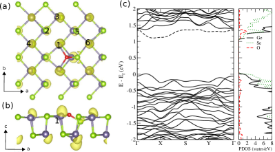
A possible relaxation route of the initial top–Se configuration is through the Se(5)–O bond stretching, which allows the oxygen to bind with the two germanium atoms of the adjacent zig-zag chain, forming a Ge2OSe bridge, as shown in Fig. 3(a) and (b). The lone pairs of the two germanium atoms bounded to the oxygen are slightly affected [Fig. 3(a) and (b)]. The charge to form the Ge–O bond comes from the Ge(1)–Se(2) bond, which breaks (stretches by 15%). This configuration is about 59% less energetically favorable than the most favorable configuration (Table 1). The oxygen defect introduces a shallow defect state near the conducting band edge [dashed line in Fig. 3(a) left], and it is essentially composed by the oxygen and nearby germanium and selenium atoms, as seen from the PDOS [red-dashed line in Fig. 3(c) right]. The absorption edge of this configuration is also blue-shifted, as the bandgap increases by 23%.
The oxidation of monolayer GeSe only through Se–O bond formation is unlikely. Indeed, the Se–O–Se configuration doest not lead to a favorable configuration (not shown), and experimental chemical composition measurements in GeSe nanosheets Mukherjee et al. (2013) indicate only Ge–O bonds. Nevertheless, oxygen binding to both germanium and selenium (Ge–O–Se) has been observed in germanium-selenide glasses.Yan et al. (2011)
In the configuration with the initial interstitial Ge(1)–Se(1) oxygen defect, the oxygen migrates to the bottom zig-zag (b-zz) chain, breaking the Ge(5)–Se(1) bond to form Ge(5)–O and Se(1)–O bonds, as shown in Fig. 4(a) and (b). The b-zz configuration is about 87% less energetically favorable than the most favorable geometry (see Table 1), but yet exothermic. The comparison of the geometries shown in Fig. 3 and Fig. 4 indicates that it is more favorable for the oxygen to form a bridge between the two adjacent zig-zag chains than to enter in the Ge(5)–Se(1) bond of a single zig-zag chain. The oxygen defect compress the Ge(1)–Se(2) bond by 3%, stretches the Se(2)–Ge(3) bond by 2%, and stretches the Ge(5)–Se(3) bond by 6%. The Se(1) is pushed by the oxygen and the lateral distance (along a–direction) between Se(1) and Se(3) is 0.67 Å. These structural modifications introduce a deep defect state in the bandgap [dashed line in Fig 4(c) left]. The bandgap increases by 15% and it becomes indirect. This defect state is essentially localized at the oxygen and nearby germanium and selenium atoms [Fig. 4(a) and (b)].
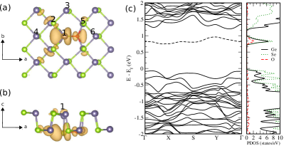
In the energetically most favorable configuration, the oxygen connects two adjacent zig-zag chains through bonds with three Ge atoms (Ge2OGe bridge). This configuration is achieved through a severe deformation of the monolayer GeSe. The Ge(1)–Se(2) and Ge(4)–Se(2) bonds break (stretched by 41% and 39%, respectively), the oxygen pulls up the Ge(2’) bonding together, and the Se(2’) moves to form the Ge(4)–Se(2’) bond. In the resulting configuration, shown in Fig. 5(a) and (b), the Ge(4) assumes a tetrahedral-like coordination, and it is bounded to four Se atoms. The oxygen defect introduces a shallow defect state near the conduction band edge [dashed line in Fig. 5(c) left]. The bandgap increases by 22% and becomes indirect. Remarkably, this band has essentially no contribution from the oxygen atom, as can be seen from the PDOS [red-dashed line in Fig. 5(c) left] and are mainly localized around the Ge(4), as shown in the LDOS [Fig. 5(a) and (b)].
IV Conclusion
The oxidation process on monolayer GeSe is investigated using first-principles calculations. Our results indicate that the oxidation of the monolayer GeSe is an exothermic process, taking place preferentially at the germanium site. The introduction of oxygen on the monolayer GeSe can result in severe local geometry deformations, giving rise to a shallow or a deep defect state within the material bandgap. Furthermore, the results suggest that oxygen defects increase the monolayer GeSe bandgap, blue-shifting its absorption edge by up to 23% and may induce direct to indirect bandgap transitions. Although the monolayer GeSe oxidation occurs naturally, if performed in a controlled way the oxidation process can possibly be a route for tunning the material electronic properties.
Acknowledgements.
The authors acknowledge support from the Brazilian agencies CNPq, FAPEMIG and the computational time spent at LCC-UFLA. R. Longuinhos thanks to J. Ribeiro-Soares, for useful discussions on the manuscript.References
- II et al. (2010) D. D. V. II, R. J. Patel, M. A. Hickner, and R. E. Schaak, Journal of the American Chemical Society 132, 15170 (2010).
- Mukherjee et al. (2013) B. Mukherjee, Y. Cai, H. R. Tan, Y. P. Feng, E. S. Tok, and C. H. Sow, ACS Applied Materials & Interfaces 5, 9594 (2013).
- DimitriD. Vaughn et al. (2012) I. DimitriD. Vaughn, D. Sun, S. M. Levin, A. J. Biacchi, T. S. Mayer, and R. E. Schaak, Chemistry of Materials 24, 3643 (2012).
- Xue et al. (2012) D.-J. Xue, J. Tan, J.-S. Hu, W. Hu, Y.-G. Guo, and L.-J. Wan, Advanced Materials 24, 4528 (2012).
- Antunez et al. (2011) P. D. Antunez, J. J. Buckley, and R. L. Brutchey, Nanoscale 3, 2399 (2011).
- Ding et al. (2015) G. Ding, G. Gao, and K. Yao, Scientific Reports , 9567 (2015).
- Survey (2002) U. G. Survey, “Rare earth elements – critical resoucers for high technology,” pubs.usgs.gov/fs/2002/fs087-02 (2002), [acesso: 20/02/2016].
- Kügeler et al. (2011) C. Kügeler, R. Rosezin, E. Linn, R. Bruchhaus, and R. Waser, Applied Physics A 102, 791 (2011).
- Bräuhaus et al. (2008) D. Bräuhaus, C. Schindler, U. Böttger, and R. Waser, Thin Solid Films 516, 1223 (2008).
- Taniguchi et al. (1990) M. Taniguchi, R. L. Johnson, J. Ghijsen, and M. Cardona, Phys. Rev. B 42, 3634 (1990).
- Elkorashy (1986) A. M. Elkorashy, physica status solidi (b) 135, 707 (1986).
- Elkorashy (1989) A. M. Elkorashy, physica status solidi (b) 152, 249 (1989).
- Hanrath et al. (2005) T. Hanrath, , and B. A. Korgel, The Journal of Physical Chemistry B 109, 5518 (2005).
- Hohenberg and Kohn (1964) P. Hohenberg and W. Kohn, Phys. Rev. 136, B864 (1964).
- Kohn and Sham (1965) W. Kohn and L. J. Sham, Phys. Rev. 140, A1133 (1965).
- Giannozzi et al. (2009) P. Giannozzi, S. Baroni, N. Bonini, M. Calandra, R. Car, C. Cavazzoni, D. Ceresoli, G. L. Chiarotti, M. Cococcioni, I. Dabo, A. D. Corso, S. de Gironcoli, S. Fabris, G. Fratesi, R. Gebauer, U. Gerstmann, C. Gougoussis, A. Kokalj, M. Lazzeri, L. Martin-Samos, N. Marzari, F. Mauri, R. Mazzarello, S. Paolini, A. Pasquarello, L. Paulatto, C. Sbraccia, S. Scandolo, G. Sclauzero, A. P. Seitsonen, A. Smogunov, P. Umari, and R. M. Wentzcovitch, Journal of Physics: Condensed Matter 21, 395502 (2009).
- Monkhorst and Pack (1976) H. J. Monkhorst and J. D. Pack, Phys. Rev. B 13, 5188 (1976).
- Perdew et al. (1996) J. P. Perdew, K. Burke, and M. Ernzerhof, Phys. Rev. Lett. 77, 3865 (1996).
- Blöchl (1994) P. E. Blöchl, Physical Review B 50, 17953 (1994).
- Jhi et al. (2000) S.-H. Jhi, S. G. Louie, and M. L. Cohen, Phys. Rev. Lett. 85, 1710 (2000).
- Chan et al. (2003) S.-P. Chan, G. Chen, X. G. Gong, and Z.-F. Liu, Phys. Rev. Lett. 90, 086403 (2003).
- Savin et al. (1997) A. Savin, R. Nesper, S. Wengert, and T. F. Fässler, Angewandte Chemie International Edition in English 36, 1808 (1997).
- Wiedemeier and von Schnering (1978) H. Wiedemeier and H. von Schnering, Zeitschrift für Kristallographie 148, 295 (1978).
- Gomes and Carvalho (2015) L. C. Gomes and A. Carvalho, Phys. Rev. B 92, 085406 (2015).
- Ziletti et al. (2015) A. Ziletti, A. Carvalho, D. K. Campbell, D. F. Coker, and A. H. Castro Neto, Phys. Rev. Lett. 114, 046801 (2015).
- Hu et al. (2015) Y. Hu, S. Zhang, S. Sun, M. Xie, B. Cai, and H. Zeng, Applied Physics Letters 107, 122107 (2015), http://dx.doi.org/10.1063/1.4931459.
- Yan et al. (2011) Q. Yan, H. Jain, J. Ren, D. Zhao, and G. Chen, The Journal of Physical Chemistry C 115, 21390 (2011).