Well separated trion and neutral excitons on superacid treated MoS2 monolayers
Abstract
Developments in optoelectronics and spin-optronics based on transition metal dichalcogenide monolayers (MLs) need materials with efficient optical emission and well-defined transition energies. In as-exfoliated MoS2 MLs the photoluminescence (PL) spectra even at low temperature consists typically of broad, overlapping contributions from neutral, charged excitons (trions) and localized states. Here we show that in superacid treated MoS2 MLs the PL intensity increases by up to times at room temperature. The neutral and charged exciton transitions are spectrally well separated in PL and reflectivity at K, with linewidth for the neutral exciton of meV, but with similar intensities compared to the ones in as-exfoliated MLs at the same temperature. Time resolved experiments uncover picoseconds recombination dynamics analyzed separately for charged and neutral exciton emission. Using the chiral interband selection rules, we demonstrate optically induced valley polarization for both complexes and valley coherence for only the neutral exciton.
Introduction.—
Transition metal dichalcogenide (TMD) monolayers (ML) such as MoS2, MoSe2, WS2 and WSe2 are a new class of two-dimensional semiconductors with a direct bandgap in the visible region of the spectrum Mak et al. (2010); Splendiani et al. (2010); Ross et al. (2013) and very unique properties. Strong spin orbit coupling combined with a crystal lattice that has no inversion symmetry allows for optical manipulation of the spin and valley degree of freedom in these materials Xiao et al. (2012). In addition to their potential for unconventional, atomically thin and flexible electronics or valleytronics, they also are ideal candidates for optoelectronic and spin-optronic applications. For example, solar cells Tsai et al. (2014),photodetectors Lopez-Sanchez et al. (2013) and laser prototypes Salehzadeh et al. (2015) based on mono or few-layer MoS2 have been demonstrated.
In these ideal 2D systems the optical properties are dominated by excitons, as the electron-hole Coulomb interaction is strongly enhanced due to quantum confinement and reduced screening Chernikov et al. (2014); Hill et al. (2015). In addition to neutral excitons (X), also charged excitons (T) contribute to the emission as ML samples are intentionally or non-intentionally doped Mak et al. (2013). Here the exciton linewidth and defect contribution to the emission is very different from one material to another. For example, at temperatures between and K ML MoSe2 shows only sharp X and T emission (FWHM 10 meV) separated by about 30 meV Ross et al. (2013). In contrast, the PL of as-exfoliated or CVD grown ML MoS2 over the same temperature range is characterized by a broad exciton peak (FWHM 60 meV) at an energy between and eV Lagarde et al. (2014); Cao et al. (2012); Kioseoglou et al. (2012); Zeng et al. (2012), which stems from overlapping T and X contributions as well as from broad low energy defects-related emission.
Very recently, Amani et al. Amani et al. (2015) have shown that the room temperature PL intensity of superacid treated ML MoS2 is two orders of magnitude higher than in as-exfoliated layers. We have used this treatment to cure exfoliated samples and find, in addition to the increased room temperature PL intensity, several important improvements of the optical quality, particularly striking at low temperature. First, the emission at K is now dominated by sharp, well separated trion and neutral exciton emission, very similar to high quality MoSe2 and WSe2 MLs Jones et al. (2013); Wang et al. (2015); Ross et al. (2013). Second, the emission at low energy related to defects is greatly suppressed. It has been found, in addition, that the PL intensity of neutral and charged excitons is similar at K in non treated and treated MLs. Nevertheless, the clear separation of the exciton and trion in treated MLs allows to probe individually valley polarization and dynamics. These experiments on cured ML MoS2 open the door for more demanding optoelectronics and spin manipulation experiments in this material, which were so far impossible to carry out due to the spectrally broad emission stemming from several different contributions.
Samples and Experimental Set-up.—
Mechanically exfoliated flakes of bulk MoS2 crystals (2D semiconductors) were transfered onto SiO2/Si substrates using a viscoelastic stamp Castellanos-Gomez
et al. (2014). The SiO2 layer ( nm thick) provides an efficient color contrast under white light illumination, allowing an easy identification of MLs. Treated samples were prepared as follows: first, the samples were annealed on a hot plate at C during 30 minutes in ambient air. Then, bis(trifluoro-methane) sulfonimide (TFSI) was dissolved on 1,2-dichloroethane (DCE) at a concentration of mg/mL, and the samples were immersed in this solution at C during 10 minutes. Finally, the samples were rinsed in DCE and annealed again during 5 minutes at C on a hot plate.
A standard micro-PL set-up is used to record the PL spectra in the temperature range K. For stationary measurements, MLs were excited with a nm cw laser. For polarization-resolved measurements, the flakes were excited by ps pulses generated by a tunable optical parametric oscillator (OPO) synchronously pumped by a mode-locked Ti:sapphire laser. For time-resolved photoluminescence experiments, the flakes are excited by ps pulses at nm generated by a tunable mode-locked frequency-doubled Ti:Sa laser with a repetition rate of MHz Lagarde et al. (2014). In all cases, the excitation spot diameter is m, i.e considerably smaller than the ML size of typically mm, and the PL emission is dispersed in a spectrometer and detected with either a cooled Si-CCD camera or a Hamamatsu C5680 streak camera for time-resolved experiments.
Results and Discussion.—
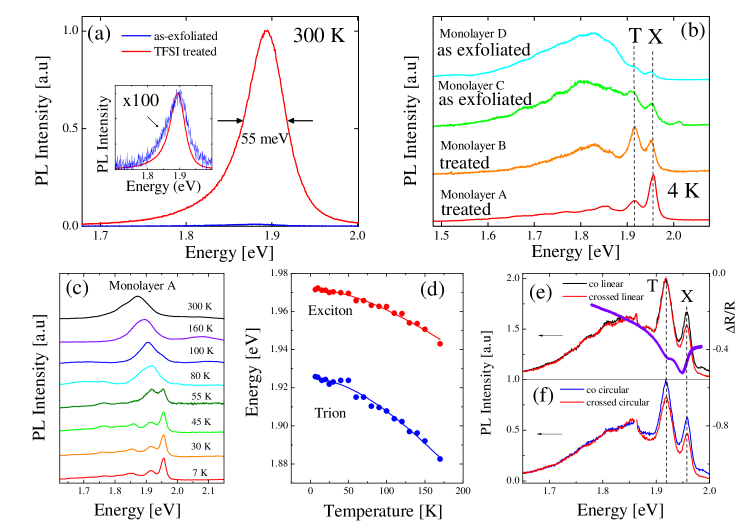
Panel (a) of Fig.1 shows the PL spectrum at room temperature for a MoS2 ML before (blue) and after acid treament (red). On 7 different samples, it is found that the spectrally integrated intensity is enhanced by 20 to 60 times on TFSI treated MoS2 MLs for a low power excitation ( W) at nm. This dramatic increase in PL efficiency is accompanied by a reduction of the linewidth (from to meV), as can be seen in the inset of Fig.1 (a) in which the PL spectrum before treatment has been amplified by two orders of magnitude for better comparison.
As shown in panel (b) of Fig.1, the typical spectrum of two as-exfoliated samples (C and D) at a temperature of K presents a broad low energy emission ascribed to defect-related trapped exciton states, which overlap strongly with exciton and trion emission, preventing a clear identification of these two peaks. In contrast, the spectra of treated samples (A and B) have a significant reduction of the low energy emission, and the neutral exciton ( eV) and trion ( eV) can be thus nicely resolved, with linewidths of and meV, respectively. In all cases, the incident laser power was kept at W. We emphasize that the same PL intensity for X and T is found for treated and as-exfoliated MLs at K. The exciton and trion separation, of meV, is larger than the meV found typically on WSe2 and MoSe2, in agreement with previous measurements Mak et al. (2013). This suggests a high non-intentional doping of the monolayer. The clean spectra of the exciton and trion in our acid treated samples cleary represent a dramatic improvement in optical quality.
The temperature dependence of the PL emission, shown in panel (c) of Fig.1 for a treated sample (A) suggests that both X and T contribute to the spectrum at room temperature, in agreement with the findings of Mak et al.Mak et al. (2013). This provides a possible explanation to the very high sensitivity of MoS2 to dielectric environment, gate voltages and even physisorption of air molecules, which can cause efficient charge tuning on the monolayer and therefore an important modulation of the PL intensity Tongay et al. (2013); Mak et al. (2013). This is a major difference with standard MoSe2 and WSe2 MLs in which the T contribution vanishes above K Robert et al. (2016). The variation of both X and T energy position with temperature, shown in panel (d) of Fig.1 can be well reproduced by the Varshni relation:
| (1) |
Solid lines in panel (d) of Fig.1 are fits to our data, with the parameters meV/K and meV/K for X and T, respectively, and K, similar to the fitting parameters found by Kioseoglou et al.Kioseoglou et al. (2012), although only one broad peak at the trion energy was observed in that study at all temperatures.
Both X and T transitions can also be identified by the differential reflectivity spectrum, defined as and shown in panel (e) of Fig.1 (violet curve). Indeed, both transitions are related to a high density of states, whereas no signature of transitions at the energy of the localized emission is visible.
We now focus on the ability to study the polarization properties of X and T lines separately, which has been elusive so far in MoS2.
In TMD MLs, the circular polarization of an absorbed/emitted photon can be directly associated with selective carrier excitation/population in one of the two non-equivalent K valleys of the Brillouin zone, or . As shown in Fig.1 (f),
both exciton and trion peaks of a treated monolayer exhibit large circular polarization in PL under circular excitation at eV, while the localized states emission is largely unpolarized, in agreement with previous measurements in as-exfoliated MLs Lagarde et al. (2014); Mak et al. (2012).
Whereas excitation with circularly polarized light initialize valley polarization, excitation with linearly polarized light results in exciton alignment, also termed valley coherence Jones et al. (2013). In Fig.1 (e) we show linearly polarized emission of the X following linearly polarized excitation. No linear polarization is observed for the peak we attribute to the trion, as can be expected for this three-particle complex. The linear polarization analysis observed in our cured samples allows us to confirm the attribution of the two sharp peaks to X and T complexes.
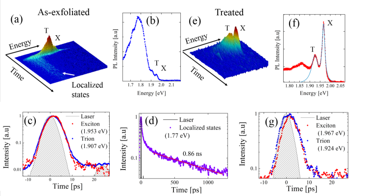
Time-resolved photoluminescence was performed in order to study the dynamics for X and T complexes separately. The time-averaged laser power was kept in the W range in order to avoid sample degradation. Panel (a) of Fig.2 shows a 3D representation of the time resolved emission for an as-exfoliated MoS2 monolayer at K, which presents, in addition to a broad trion peak and a smaller exciton feature, a slowly decaying shoulder at lower energies which corresponds to localized excitons Lagarde et al. (2014). Panel (b) of Fig.2 shows that the time-averaged spectrum is dominated by this localized emission that hinders the identification of trion and exciton peaks, both presenting a decay with a very fast dynamics, as can be inferred from the profiles shown in panel (c) of Fig.2. The localized emission’s temporal evolution, shown in panel (d), has a decay lifetime on the ns scale. When time-resolved measurements are performed on treated MLs, the emission of localized states is highly suppressed, and emission comes mainly from well defined exciton and trion peaks, shown in panels (e) and (f) of Fig.2. Note that in this particular flake, exciton emission is more intense than trion’s, probably caused by an important depletion of the unintentional n-doping. Again, a very short emission time of ps, almost limited by our temporal resolution, is observed for the exciton and trion (panel (g)), just like in as-exfoliated MoS2 samples. This demonstrates that the low temperature exciton dynamics in treated and non-treated MLs is not dominated by non-radiative recombination on the defects which are suppressed by the acid treatment. This exciton dynamics can be interpeted by a fast radiative decay at low temperatures as a result of the strong exciton oscillator strength in TMDC MLs, which is consistent with recent measurements performed on MoSe2 and WSe2 MLsRobert et al. (2016), and theoretical predictions Wang et al. (2016); Palummo et al. (2015).
Perspectives.—
In conclusion, MoS2 monolayers have been treated with TFSI superacid. In addition to the enhancement of the PL intensity by nearly two orders of magnitude at room temperature, it has been shown that there is a significant reduction of localized states emission at low temperatures, allowing to obtain well resolved emission for both exciton and trion complexes. This should open the door for a better understanding of the exciton physics on ML MoS2, an ideal candidate for atomically thin opto-electronic devices.
Acknowledgements.—
We thank ANR MoS2ValleyControl and ERC Grant No. 306719 for financial support. X.M. also acknowledges the Institut Universitaire de France. F.C and P. R thank the grant NEXT
No ANR-10-LABX-0037 in the framework of the « Programme des Investissements d’Avenir”.
References
- Mak et al. (2010) K. F. Mak, C. Lee, J. Hone, J. Shan, and T. F. Heinz, Phys. Rev. Lett. 105, 136805 (2010).
- Splendiani et al. (2010) A. Splendiani, L. Sun, Y. Zhang, T. Li, J. Kim, C.-Y. Chim, G. Galli, and F. Wang, Nano Letters 10, 1271 (2010).
- Ross et al. (2013) J. S. Ross, S. Wu, H. Yu, N. J. Ghimire, A. M. Jones, G. Aivazian, J. Yan, D. G. Mandrus, D. Xiao, W. Yao, et al., Nature communications 4, 1474 (2013).
- Xiao et al. (2012) D. Xiao, G.-B. Liu, W. Feng, X. Xu, and W. Yao, Phys. Rev. Lett. 108, 196802 (2012).
- Tsai et al. (2014) M.-L. Tsai, S.-H. Su, J.-K. Chang, D.-S. Tsai, C.-H. Chen, C.-I. Wu, L.-J. Li, L.-J. Chen, and J.-H. He, ACS Nano 8, 8317 (2014).
- Lopez-Sanchez et al. (2013) O. Lopez-Sanchez, D. Lembke, M. Kayci, A. Radenovic, and A. Kis, Nature Nanotechnology 8, 497–501 (2013).
- Salehzadeh et al. (2015) O. Salehzadeh, D. Mehrdad, N. H. Tran, I. Shih, and Mi, Nano Letters 15, 5302 (2015).
- Chernikov et al. (2014) A. Chernikov, T. C. Berkelbach, H. M. Hill, A. Rigosi, Y. Li, O. B. Aslan, D. R. Reichman, M. S. Hybertsen, and T. F. Heinz, Phys. Rev. Lett. 113, 076802 (2014).
- Hill et al. (2015) H. M. Hill, A. F. Rigosi, C. Roquelet, A. Chernikov, T. C. Berkelbach, D. R. Reichman, M. S. Hybertsen, L. E. Brus, and T. F. Heinz, Nano Letters Article ASAP, null (2015).
- Mak et al. (2013) K. F. Mak, K. He, Changgu, G. H. Lee, J. Hone, T. F. Heinz, and J. Shan, Nature Materials 12, 207 (2013).
- Lagarde et al. (2014) D. Lagarde, L. Bouet, X. Marie, C. R. Zhu, B. L. Liu, T. Amand, P. H. Tan, and B. Urbaszek, Phys. Rev. Lett. 112, 047401 (2014).
- Cao et al. (2012) T. Cao, G. Wang, W. Han, H. Ye, C. Zhu, J. Shi, Q. Niu, P. Tan, E. Wang, B. Liu, et al., Nature Communications 3, 887 (2012).
- Kioseoglou et al. (2012) G. Kioseoglou, A. T. Hanbicki, M. Currie, A. L. Friedman, D. Gunlycke, and B. T. Jonker, Applied Physics Letters 101, 221907 (pages 4) (2012).
- Zeng et al. (2012) H. Zeng, J. Dai, W. Yao, D. Xiao, and X. Cui, Nat. Nanotechnol. 7, 490 (2012).
- Amani et al. (2015) M. Amani, D.-H. Lien, D. Kiriya, J. Xiao, A. Azcatl, J. Noh, S. R. Madhvapathy, R. Addou, S. KC, M. Dubey, et al., Science 350, 1065 (2015), ISSN 0036-8075.
- Jones et al. (2013) A. M. Jones, H. Yu, N. J. Ghimire, S. Wu, G. Aivazian, J. S. Ross, B. Zhao, J. Yan, D. G. Mandrus, D. Xiao, et al., Nat. Nanotechnol. 8, 634 (2013).
- Wang et al. (2015) G. Wang, X. Marie, I. Gerber, T. Amand, D. Lagarde, L. Bouet, M. Vidal, A. Balocchi, and B. Urbaszek, Phys. Rev. Lett. 114, 097403 (2015).
- Castellanos-Gomez et al. (2014) A. Castellanos-Gomez, M. Buscema, R. Molenaar, V. Singh, L. Janssen, H. S. J. van der Zant, and G. A. Steele, 2D Materials 1, 011002 (2014).
- Tongay et al. (2013) S. Tongay, J. Zhou, C. Ataca, J. Liu, J. S. Kang, T. S. Matthews, L. You, J. Li, J. C. Grossman, and J. Wu, Nano Letters 13, 2831 (2013).
- Robert et al. (2016) C. Robert, D. Lagarde, F. Cadiz, G. Wang, B. Lassagne, T. Amand, A. Ballochi, P. Renucci, S. Tongay, B. Urbaszek, et al., ArXiv e-prints 1603.00277 (2016).
- Mak et al. (2012) K. F. Mak, K. He, J. Shan, and T. F. Heinz, Nat. Nanotechnol. 7, 494 (2012).
- Wang et al. (2016) H. Wang, C. Zhang, W. Chan, C. Manolatou, S. Tiwari, and F. Rana, Phys. Rev. B 93 (2016).
- Palummo et al. (2015) M. Palummo, M. Bernardi, and J. C. Grossman, Nano Letters 15 (2015).