Resonant plasmonic terahertz detection in graphene split-gate field-effect transistors with lateral p-n junctions
Abstract
We evaluate the proposed resonant terahertz (THz) detectors on the base of field-effect transistors (FETs) with split gates, electrically induced lateral p-n junctions, uniform graphene layer (GL) or perforated (in the p-n junction depletion region) graphene layer (PGL) channel. The perforated depletion region forms an array of the nanoconstions or nanoribbons creating the barriers for the holes and electrons. The operation of the GL-FET- and PGL-FET detectors is associated with the rectification of the ac current across the lateral p-n junction enhanced by the excitation of bound plasmonic oscillations in in the p- and n-sections of the channel. Using the developed device model, we find the GL-FET and PGL-FET-detectors characteristics. These detectors can exhibit very high voltage responsivity at the THz radiation frequencies close to the frequencies of the plasmonic resonances. These frequencies can be effectively voltage tuned. We show that in PL-FET-detectors the dominant mechanism of the current rectification is due to the tunneling nonlinearity, whereas in PGL-FET-detector the current rectification is primarily associated with the thermionic processes. Due to much lower p-n junction conductance in the PGL-FET-detectors, their resonant response can be substantially more pronounced than in the GL-FET-detectors corresponding to fairly high detector responsivity.
I Introduction
The lateral p-n-junctions in field-effect transistor (FET) structures with a graphene layer (GL) channel and split gates 1 ; 2 ; 3 ; 4 ; 5 ; 6 can be used in new electron and optoelectronic devices. For example, the tunneling electron-transit diodes for generating terahertz radiation (THz) 7 ; 8 , interband THz photodetectors 9 ; 10 ; 11 ; 12 ; 13 ; 14 ; 15 ; 16 ; 17 ; 18 , and injection THz lasers 19 ; 20 ; 21 have been proposed and analyzed. Recently 22 , the THz emission from split-gate GL-FET structures with forward biased p-n- junctions was observed. Similarly, graphene nanoribbon (GNR) and graphene bilayer (GBL) FET structures with p-n junctions can be used in different devices 23 ; 24 ; 25 ; 26 ; 27 ; 28 . The nonlinearity of the current-voltage characteristics of the GL 1 ; 4 ; 26 ; 27 ; 28 ; 29 and GBL p-n-junctions 30 ; 31 ; 32 ; 33 can be used for detecting THz radiation using the effect of the current rectification and for the THz generation using the tunneling negative differential conductivity. Since the gated regions of p- and n-types form the plasmonic cavities 34 , the excitation of the plasmonic oscillations (the oscillations of the electron or hole density and the self-consistent electric field) by incoming THz radiation can substantially affect the detector characteristics due to the plasmonic resonances. An idea to use the plasmonic properties of the electron (or hole) system in the channel of a FET for the resonant THz detection was brought forward a long time ago 34 . The key points of this idea are: (1) the resonant excitation of the plasmonic oscillations and (2) the rectification of the ac current is due to the hydrodynamics nonlinearity of the electron system dynamics in the channel. Later, the concept of FET-based THz detectors was successfully realized and such detectors based on III-V compound materials with the enhanced characteristics were manufactured and used in applications (see, for example, 35 ; 36 ; 37 ; 38 ; 39 ). The concepts of using the combination of plasmonic effects and other types of the current nonlinearity (stronger than the hydrodynamic nonlinearity) were also considered.
Due to unique electron properties of GLs, GNR, and GBLs 40 ; 41 ; 42 ; 43 and a remarkable progress in fabrication of different transistor heterostructures based on GLs, such FETs can be used for THz detectors (and frequency multipliers) with enhanced performance 44 ; 45 ; 46 ; 47 . The advantages of the GL-based heterostructures are associated with the enhanced mobility at room temperature (about 110,000 cm2/V s in the epitaxially grown GLs on SIC substrate 43 ). This leads to a high quality factor of the plasmonic oscillations at room temperature and high frequencies of the plasma modes in relatively long channels due to the elevated plasma-wave velocity 48 . Besides higher room-temperature quality factors compared to those for the FET-detectors based on the standard materials, the symmetry of the hole and electron energy spectra provides an opportunity to realize coherent coupled plasmonic oscillations in the p- and n-sections of the device. The vertical GL-based structures can also be used for the resonant plasmonic THz detection 49 ; 50 . The GNR transistor structures 23 ; 51 can serve the basis for the THz detectors using different operational principles 14 , including the resonant absorption of THz radiation 53 ; 54 leading to the rectification and bolometric effects. High quality factor of the plasmonic oscillations in GL-heterostructures, opens up the prospect of realization of the room-temperature THz detectors exhibiting pronounced resonant behavior due to the plasmonic effects with very high peak responsivity and strong spectral selectivity.
In this paper, we evaluate the proposed resonant THz detector based on lateral split-gate GL-FET and split-gate FET with the GL perforated between the gates (PGL-FET) in which the channel is partitioned into the p- and n-type sections.
The operation of such detectors is enabled by the nonlinearity of the p-n-junction and the excitation of coupled plasmonic oscillations in the gated channel sections. We demonstrate that the responsivity of the GL-FETs under consideration as function of the incoming THz radiation frequency can exhibit the resonant response. However, the height of the spectral dependence responsivity peaks and their sharpness are rather moderate. This is because of relatively high conductance of the p-n junction in the GLs associated with the interband tunneling can be compared with the conductance of the channel. In contrast, in the PGL-FETs the tunneling mechanism can be effectively suppressed by appropriate choice of the energy gap in the perforated portion of the channel (perforated depletion region of the p-n junction). Apart from this, the thermionic conductance of the p-n junction is also limited by the channel nanoconstrictions. As a result, the net conductance of the p-n junction can be much smaller than that of the gated channel sections that is beneficial for the achievement of pronounced spectral selectivity and elevated peak responsivity.
II Device model
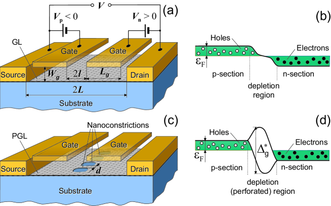
In FETs with undoped GL-channel and with the split gates, the formation of the lateral p-n junction is realized by applying voltages and between the source and the neighboring gate section (source gate section) and between the drain and the drain gate section. Figure 1 shows the GL- and PGL-FETs, which can be used for the THz detection and their band diagrams at properly chosen applied gate voltages.
The main feature of the PGL-FETs is the energy band gap in the depletion region caused by the GL perforation substantially affecting the conductivity, nonlinear, and plasmonic properties of the p-n-junction (as in FETs based on heterostructure made of the standard materials 55 ; 56 ). This region can be considered as an array of the nanoconstrictions or GNRs similar to the GNR channels of FETs 51 and bolometric detectors 52 . The source-drain voltage comprises the dc and ac signal components: is applied between the side contacts, where is the dc bias voltage in the case of photocurrent detection and the dc signal voltage produced by the incoming radiation in the photovoltaic regime, and are the amplitude and frequency of the ac signal received by an antenna.
We assume that the steady-state hole and electron densities in the GL channel, and , are equal to each other: . If, in addition, both the gates have similar length, , and due to the symmetry of the hole and electron energy spectra, the plasmonic properties of the p- and n-channel sections are similar. In this case, the plasmonic oscillations in the p- and n-channel sections can be synchronized.
If the length of the gates and the net length of the channel () are markedly larger than the gate layers thickness , one can apply the gradual channel approximation 57 . Assuming that the two-dimensional hole system (2DHS) in the p-section and two-dimensional electron system (2DES) in the n-section of the GL channel are degenerate, one can write down the following equations for the hole (in the p-section) and electron (in the n-section) density in the undoped channel (at zero Dirac point):
| (1) |
Here we set , is the electron charge, is the dielectric constant of the gate layer material, and is the hole and electron Fermi energy in the pertinent channel sections. The Fermi energy is equal to , where cm/s is the characterisctic velocity of electrons and holes in GLs, and is the Planck constant. The term with in the right-hand side of equation (1) is associated with the effect of the quantum capacitance 58 . The hole and electron systems degeneracy implies that , where is the temperature (in the energy units).
Consequently, the small-signal variations of the hole density and the electron density caused by the ac variations of the electric potential in the channel are given by
III Thermionic and tunneling conductance and parameter of nonlinearity
The ac source-drain current is determined by the admittances of the p- and n- sections of the channel and the p-n-junction. The net ac current density through the p-n-junction (the current per unit length in the direction along the gate edges) at the signal frequency , associated with the ac voltage between the source and drain contacts induced by the incoming radiation, includes the ac interband tunneling and thermionic components and , respectively, and the displacement component :
| (3) |
The latter term in Eq. (3) is given by
| (4) |
where is the geometrical capacitance of the lateral p-n-junction under consideration, being the length of the depletion region (which is comparable with the spacing between the gate edges) in the p-n-junction (see, for example, 61 ), and are the ac electric potentials of the quasi-neutral p- and n-sections at their edges and , respectively, and the axis is directed from source to drain.
The ac current density associated with the tunneling and thermionic processes caused by the ac signal can be presented as
| (5) |
The the variation of the dc current density , , arising from the averaging of the nonlinear components of the ac current density and the ac voltage drop across the p-n-junction over the fast oscillations (the rectified current and voltage components), is given by
| (6) |
In Eqs. (6) and (7),
| (7) |
where is the dc current through the p-n junction at the dc source-drain voltage (bias voltage or radiation induced voltage) . The quantities and are the p-n-junction differential conductance (i.e., the real part of its net conductance ) and the parameter of nonlinearity of the p-n junction current-voltage characteristics (leading to the rectification and frequency doubling effects), respectively. The latter formulas are valid when the space-charged (depletion) region of the p-n junction is sufficiently narrow, so that the characteristic time of electron and hole transit across this region is small in comparison with the inverse signal frequency , In the opposite case, for example, at sufficiently strong the reverse bias, so that can be relatively large, and can be the frequency dependent (i.e., and ) due to the electron and hole transit-time effects 7 ; 8 (see Section VIII). Considering both the interband tunneling and the thermionic contributions, one can obtain
| (8) |
Here the first and the second terms in equation (9) describe the contributions of the tunneling and thermionic processes, respectively. Considering equations (A5), (A6), (A9), and (A10) in the Appendix A, for the GL-FETs and we arrive at
| (9) |
| (10) |
where is the electron and hole temperature in the channel (which we equalize to the lattice temperature) in the energy units, The quantities and describe the relative contributions of the intersection tunneling (see the Appendix A). In the GL-FETs,
| (11) |
| (12) |
where is the effective width of the p-n junction. Deriving equations (11) and (12), we have accounted for that the GL p-n-junction built-in voltage , set for simplicity the built-in electric field in the p-n-junction depletion region equal to with considered as a phenomenological parameter (see the Appendix A) and assumed that the dc voltage is created only by the rectification effect, i.e., it is small (the photo-voltaic detection).
In the PGL-FETs, the densities of the displacement, hole, and electron currents are spatially periodic in the direction along the gate edges. Considering the PGL-FETs with the period of the perforation of the depletion region , we average these current densities, conductances, and the parameter of nonlinearity over short-range periodical spatial variations. Taking this into account, for the PGL-FETs the quantity averaged over the periodic spatial variations is presented as (see the Appendix B)
| (13) |
| (14) |
Here the quantity is the activation energy of the thermionic transitions between the channel sections through the channel nanoconstrictions between the perforations (GNRs), is the energy gap in these nanoconstrictions, is their width, is the number of the nanoconstrictions per unit length, is a numerical factor, which is determined by the shape of the energy barrier in the nanoconstrictions ( and for the sharp trapezoidal and smooth barriers, respectively), and is a small parameter describing the limitation of the current across the p-n-junction due to the nanoconstrictions. If m-1 and , at room temperature one obtains .
Since the incorporation of the nanoconstrictions is aimed to substantially decrease the p-n-junction conductance in comparison with the conductances of the gated sections of the channel, we assume in the following that the length of GNRs and their energy gap are sufficiently large, so that the hole and electron tunneling through them is suppressed. In line with this, for PGL-FETs we set (see the Appendix B).
IV Low-frequency GL-FET and PGL-FET detector responsivity
The current (in A/W units) and voltage (in V/W units) detector responsivities, and , to the incoming signals with the frequency are defined as
| (15) |
Here is the variation of the dc current associated with the current rectified component, is the lateral size of the device in the direction along the gate edges, is the rectified dc voltage between the side contacts induced by the received signals, which is somewhat smaller than the rectified voltage component across the p-n junction , hence, in the photovolataic regime, . The quantities , and are the wavelength of the incident THz radiation and its intensity.the intensity, where is the speed of light in vacuum and is the antenna gain. The quantities and are related to each other as .
The quantities and are proportional to , which, in turn, is determined by the spatial distributions of the ac potentials . The latter is found taking into account that
| (16) |
At relatively low signal frequencies (), the hole and electron densities as well as the electric potential manage to follow the variations of the potential at the contacts. In this case, the ac potentials in the gated channel sections at are linear functions of the coordinate along the channel:
| (17) |
with
| (18) |
Here is the ratio of the p- and n- junction differential conductance and the net dc conductance of the p- and n-sections (, see Fig. 1) with
| (19) |
so that , where is the electron and hole collision frequency in the pertinent section associated with the scattering on impurities and acoustic phonons. A schematic view of the potential distribution at low frequencies is shown (for ) in the inset in Fig. 2.
As a result, the quantities and given by Eq. (6) are equal to
| (20) |
As seen from Eq. (20), it is desirable that the quantity , i.e., the conductance of the gated sections of the channel markedly exceeds the differential conductance of the p-n-junction,
Equations (15) and (20) yield the following formula for the low-frequency current responsivity:
| (21) |
Considering equation (21) and using equations (9), (10), and (12) for and , we find for the low-frequency current responsivity of the GL-FET detectors
| (22) |
The low-frequency current responsivity of the PGL-FET detectors is given by
| (23) |
In equations (21) and (22), and , respectively, with (or ) and . Due to a relatively large value of (because of the contribution of the tunneling in the GL-FETs) and large ratio of the ”thermionic” exponential factors in equations (22) and (23), the current responsivity of the GL-FET detectors substantially exceeds that of the PGL-FET detectors.
In the photo-voltaic regime, the current density is compensated by the dc current caused by the induced dc voltage . Considering this and taking into account that the net channel dc resistance , we obtain
| (24) |
Hence, the dc voltage induced by the THz radiation between the source and drain contact is equal to
| (25) |
Considering this and using equations (20), for the voltage responsivity we obtain following formula valid for the detectors of both types:
| (26) |
Consequently,
| (27) |
with and
| (28) |
with , where .
As follows from equation (27), the enhancement of the tunneling probability (an increase of the quantity in the GL-FETs results in a decrease in the . Thus the tunneling through the p-n junction plays a negative role. This is because the tunneling component of the p-n junction conductance can exceed the thermionic component at small providing relatively low p-n junction resistance. A rise of the tunneling conductivity is accompanied by a relatively slow increase in the tunneling nonlinearity parameter .
At the realistic parameters, , so that . Taking into this condition, for the low-frequency voltage responsivities we obtain
| (29) |
The estimates for the low-frequency responsivities of the GL-FET and PGL-FET detectors at room temperature, meV, , (in the PGL-FETs with sufficiently long nanoconstrictions and properly chosen their the energy gap) yield V/W () and V/W, respectively.
V Plasmonic oscillations in GL- and PGL-FETs
At higher frequencies, the reactive components of the two-dimensional hole system (2DHS) and two-dimensional electron system (2DES) ac conductivity (which correspond to the inertia of the electron and hole motion 61 ) , the p-n-junction conductance, and the gate-channel capacitances become more important because they can subtantially affect the spatio-temporal distributions of the ac potential in the different portions of the channel. In this situation, one needs to determine accounting for these factors. We find the spatial distributions of in the GL plane (along the axis ) and, in particular , , from the linearized kinetic 48 or the hydrodynamic equations for the gated 2DHS and 2DES 62 ; 63 (adopted for the energy spectra of the electrons and holes in GLs) coupled with the Poisson equation in the gradual channel approximation, i.e., equation (2). As a result, we arrive at the following system equations:
| (30) |
Here is the characteristic plasma-wave velocity in the gated GL structures 48 ; 61 . The boundary conditions for Eqs. (29) and (30) are given by Eq. (16) (at the side contacts and the following conditions at :
| (31) |
where is given by equation (3) and the following ones and we . Writing down equation (30), we have disregarded nonlinear terms associated with the nonlinearity of the 2DES and 2DHS dynamics (in particular, the nonlinearity of the hydrodynamic equations for the 2DHS and 2DES - we have used their linearized versions!). This is because, we focus on the GL-FET operation associated with another and stronger nonlinearity (nonlinearity of the p-n-junction current-voltage characteristics).
Equation (30) with the boundary conditions (16) and (31) yield the following formulas for the spatial distributions of ac potentials :
| (32) |
for the range for , and for . Here the wavenumber and the characteristic plasma frequency for the gated 2DES and 2DHS are given by
| (33) |
The parameter , where is the p-n junction recharging time, characterizes the ratio of the channel and p-n junction conductivities. It is given by
| (34) |
At low frequencies, equation (32) reduces to equation (16).
For the GBL-FETs, the quantities and are equal to
| (35) |
| (36) |
The parameter given by in equations (11) varies in a wide rage depending on the effective widths of the depletion region , the Fermi energy , and the temperature . At K, setting nm and meV, we obtain . When , from equation (34) we arrive at . For and , one obtains . As seen in the following, the latter parameter essentially determines the character of the plasmonic effect.
Due to the smallness of , the factor in Eq. (33) can be significant at very high frequencies. Indeed, at nm, nm, nm, , and meV, one obtains s. Hence, even for THz, one obtains .
For PGL-FETs, the quantities and for the parameter given by equation (33) [compare with equations (35) and (36)], are as follows:
| (37) |
| (38) |
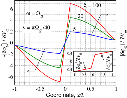
Setting , nm, nm ( meV), m-1, , meV, we obtain and s. Thus, is fairly large. Apart from this, the recharging time, , of the perforated p-n junction in the PGL-FETs is relatively long (in comparison with ) due to a small p-n junction conductance. Figure 2 schematically shows the amplitudes of the ac potential as a function of the coordinate along the channel in the devices under consideration with different values of the parameter ( or ). The radiation frequency is chosen to be equal to with and . This corresponds to the maximum span of the plasmonic oscillations. One can see from Fig. (2) that an increase in results in a substantial increase in the plasmonic oscillations, which, in turn, provides an elevated ac potential drop across the the depletion region. An example of the potential distribution shown in the inset in Fig. 2 and described by equations (16) and (17) corresponds to relatively low frequencies ().
VI Effect of plasmonic oscillations on the GL-FET and PGL-FET detectors responsivity
Equations (31) and (6) yield [compare with equation (20)]
| (39) |
where the factor
| (40) |
describes the effect of plasmonic oscillations. In the range of low frequencies , the plasmonic factor tends to , and the quantities in equation (38) coincide with those given by equation (20). As a result, for the PGL-FET detectors we can use the following formula:
| (41) |
As follows from equations (40) and (41), the plasmonic factors and , as well as the pertinent responsivities and are generally oscillatory functions of . The oscillations of and can be pronounced, i.e., the pertinent maximuma are high and sharp if the quality factor is sufficiently large.
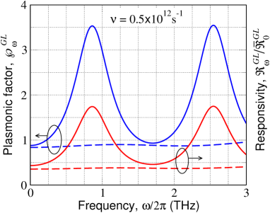
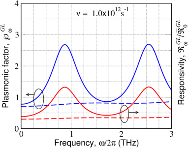
Figures 3 and 4 show the frequency dependences of the plasmonic factor calculated using equations (40) and (41) with equations (33) - (36) for s-1, and s-1. It is assumed that nm, meV, and for solid lines and nm and nm for dashed lines. In particular, if (SiC or MoS2 gate layer) and (Hf02 gate layer), the solid lines with pronounced maxima, correspond to and nm, respectively. The solid lines in figures 2 and 3 can also be attributed to the devices with hBN or SiO2 gate layers of the thickness nm.
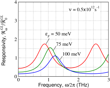
Figure 5 shows the normalized GL-FET detector responsivity as a function of the signal frequency calculated for different Fermi energies of holes and electrons, i.e., their different densities for the same other parameters corresponding to the solid lines in figure 2.
The pronounced resonant peaks in figures 3 - 5 correspond to the frequencies , where is the plasmonic mode index.
Larger values of the quality factor correspond to higher peaks of the plasmonic factor and the GL-FET detector responsivity. In particular, solid lines correspond from (in figure 3) and (in figure 4). However, the comparison of the resonant peaks in figures 3 and 4 shows that an increase in the quality factor (twice) leads only to a modest increase in the peak heights. The point is that the spectral behavior of and is also determined by the parameter characterizing the ratio of the p-n junction and the channel resistances. In particular, the data in Figs. 3 and 4 correspond to fairly moderate values of : for solid lines and for dashed lines. This is the manifestation of the effect of relatively high conductance of the p-n junction in GL-FETs, which drops when decreases. The role of this effect also reveals in the fact that seen in figures 2 - 4.
In the PGL-FETs the parameters and can be very large due to relatively small the p-n junction conductance and negligible contribution of the tunneling mechanism ().
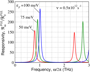
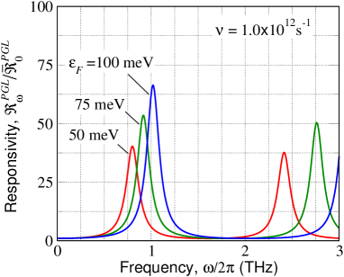
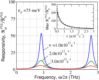
Figures 6 and 7 show the spectral dependences of the normalized responsivity of PGL-FET detectors with different hole and Fermi energy energy the energy gap in the constrictions meV ( nm), and their density m-1 calculated using equations (39) and (40) with equations (36) and (37). It is assumed that s-1 and s-1, nm, , nm, , and (). The lines for meV in figure 5 and in figure 6 correspond to the same parameters of the gated sections in the PGL- and GL-FETs. Comparing figures 6 and 7, one can see that the height of the resonant responsivity peaks markedly drops with increasing hole and electron collision frequency . This is also seen from figure 8, which demonstrates how the spectral dependence of the PGL-FET-detector normalized varies when the changes. As seen, when increases threefold, the height of the first resonant peak () drops nine times. Such a roll-off corresponds to [see the solid and dashed lines in the inset in figure 8].
VII Comparison of GL- and PGL-FET detectors
The variation of in rather wide range meV at fixed does not lead to a marked change in the spectral dependences of .
It is clearly seen that the plasmonic response of the PGL-FETs is much more pronounced than that of the GL-FETs (at similar parameters of the gated channel sections).
Equation (40) for the plasmonic factor at the frequencies when yields
| (42) |
At , one obtains
| (43) |
Hence, for both GL- and PGL-FETs, . Taking into account equation (40), for the responsivity at , one can obtain
| (44) |
for GL-FETs, and
| (45) |
for PGL-FETs.
Using equation (44) and taking into account a long rechrging time in the GL-FETs, for their responsivity in the fange of several THz, we find
| (46) |
Thus, the height of the GL-FET detector responsivity maxima is determined by min. Substituting to equation (46) the data used for the dependences shown in figures 3 and 4, we naturally obtain the same values of the peak height as in these plots.
Since the quantity can be much larger than ,for the low-index resonances equation (45) can be simplified:
| (47) |
The dependence at the realistic parameters is also confirmed by the proximity of the solid and dashed lines in the inset in figure 8.
Comparing equations (46) and (47), one can find that the responsivity peaks of the GL- and PGL-FET detectors (1) exhibit rather different height and sharpness and (2) change variously with increasing .
First, assuming that in reality , disregarding for simplicity the ”recharging” terms in the denominators of equations (44) and (45), taking into account equations(29), we find
Second, decreases with increasing , while increases. Indeed, according to Eq. (45) with Eqs. (11) and (34) at large values of and , one obtains . Such a decreasing dependence on is associated with both a decrease in the tunneling nonlinearity parameter and in an increase in the p-n junction conductance. In contrast, . Different behavior of the resonant peaks clearly seen comparing figures 5 and (6). A sensitivity of the responsivity maxima to the Fermi energy implies an opportunity to optimize the PGL-FET detector characteristics.
The peaks heights can markedly roll-off with increasing resonance index , especially if is not too small. One needs to mention that and the second term in the denominator in equation (45) is approximately proportional to , whereas both these quantities are independent of . At very high Fermi energies, the dependence versus saturates and results in the limit
VIII Comments
In the above calculations we disregarded possible frequency dispersion of the p-n junction conductance, which actually contain the factor , where is the Bessel function and (in the GL-FETs) and (in the PGL-FETs) are the transit times across the depletion region. Such a transit-tme effect might be important at the frequencies commensurable with the inverse hole and electron time when the argument of the Bessel function is about of 2 or more). At THz, nm, and meV, one obtains . Hence, the assumption that Re is independent of the frequency used in our model is valid.
The incident THz radiation heats the 2DHS and 2DES due to the Drude and the interband absorption. The variation of the hole and electron effective temperature can lead to the dc source-drain current if the device is asymmetric. The latter can be achieve by applying of the bias voltage. This effect can be used for the so-called photothermoelectric detection 52 ; 54 . However, in the case of symmetric structure in the absence of the dc bias (considered above), the effective hole and electron temperatures in the pertinent sections of the channel are equal, and, hence, the photothermoelectric effect can be disregarded (in contrast to the voltage-biased p-n junctions 52 ).
Apart from using the engineered band gap (as in the PGL-FETs under consideration), an effective suppression of the interband tunneling in the GL-FET p-n junction can also be achieved by using the saw-shaped gate electrodes instead of conventional bar-like gate electrodes 64 ; 65 ; 66 ; 67 . In such a case, the dramatically reinforced hole and electron backscattering from the barrier in the p-n junction can lead to a substantial drop in the tunneling current and the p-n junction net conductance. The GL-FET detectors with the saw-shaped gate electrodes arebeyond the scope of the present paper, need a separate consideration, and will be considered elsewhere.
IX Conclusions
In summary, we considered the proposed resonant THz detectors using FETs with the split gates, which electrically induce the lateral p-n junction in uniform and perforated GLs, GL-FET and PGL-FET detectors. The gated regions of the GL- and PGL-FETs play the role of plasmonic resonat cavities whereas the p-n junction depletion GL or PGL region enable the nonlinearity of the current-voltage characteristics. We calculated the responsivity the spatial distributions of the ac and rectified components of electric potential thermionic and tunneling currents caused by the incident THz radiation. Relating the rectified voltage component and the intensity of the THz radiation, we obtained formulas for the responsivity of the GL-FETs and PGL-FETs operating as the photovoltaic THz detectors. As shown, the spectral dependences of the responsivity can exhibit sharp resonant maxima associated with the excitation of plasmonic oscillations. The height of the responsivity peaks is determined by the hole and electron collision frequency in the channel section and by the relative conductance of the p-n junction. Due to a suppression of the tunneling current in the PGL-FETs (with the perforated p-n-junction), their resonant response is much more pronounced and the responsivity is substantially higher than that in GL-FETs The PGL-FET detectors operating at room temperature can be of interest for different THz communication systems.
Acknowledgements.
One of the authors (VR) thanks D. Svintsov for useful discussion and N. Ryabova for assistance. The work was supported by the Japan Society for Promotion of Science (Grant GA-SR-A 16H02336) and the Russian Scientific Foundation (Project 14-29-00277). The works at RPI was supported by the US Army Research Laboratory Cooperative Research Agreement.Appendix A. Differential conductance and nonlinearity parameter in GL-FETs
Thermionic (activation) current. Both the thermionic transfer of the carriers and their tunneling between the gate sections enable the nonlinear current voltage characteristics of the p-n junction. Using the Landauer-Buttiker formula 68 for 2D channels with the barrier transparency is given
| (A1) |
where is the unity step function, and considering that the thermionic current is created by both the injected electron and hole components, for the thermionic current density one can obtain
| (A2) |
Here is the signal voltage across the p-n junction, which includes the ac and rectified components, and , respectively, and he saturation current density is given by
| (A3) |
Here is the electron and hole temperature in the channel (in the energy units) and has been taken into account that the built-in voltage .
As a result, at , from Eqs. (A1) and (A2) calculating and t, we arrive at Eqs. (9) and (10).
Tunneling current. Considering that the net electric field in the p-n junction is equal to , where and are the electric fields produced built-in voltage and the signal electric field component, the tunneling current density in the GL-FETs, which is proportional to 1 ; 4 ; 8 , can be presented as
| (A4) |
Here
| (A5) |
If the spacing between the gate edges , the electric potential in the region can be presented as , where . Hence,
| (A6) |
When , neglecting the electron and hole space charges in the region and taking into account the smallness of the screening length nm 21 ; 24 ; 69 , the electric-field spatial distribution in this region is given by 8 ; 59 :
| (A7) |
Therefore , . The electron and hole space charge decrease the electric field in the p-n junction center 8 ; 21 ; 60 , so that one can put , where . Considering this, we find that and are equal to
| (A8) |
| (A9) |
respectively.
From equations (A8) and (A9) for the parameters and defined by equation (8) in the main text, considering equations (9) and (10), we obtain equations (11) and (12).
Appendix B. Differential conductance and nonlinearity parameter in PGL-FETs
Thermionic injection: sharp barrier. If the barrier in the depletion layer associated with the nanoconstrictions is sufficiently sharp, its shape can be approximated by a trapezoid. In this case, equation (A1) should be replaced by
| (B1) |
where , is the density of the nanoconstrictions, and is the energy gap in the nanoconstrictions. Calculating and , from equation (B1) we get equations (13) and (14) which accounts for the 1D transport in the nanoconstrictions and the exponential factor inherent to the activation processes.
Tunneling current: sharp barrier. Assuming that the hole and electron dispersion lows in the constrictions (GNRs) are (where ) and using the Landauer-Buttiker formula 68 for 1D channels with the tunneling transparency of the trapezoid barrier in the PGL-FET perforated region derived in the WKB approximation, we find
| (B2) |
(for ). Consequently,
| (B3) |
Comparing the thermionic and tunneling contributions, one can find that in the case of the trapezoid tunneling barrier (), the former contribution substantially exceed the tunneling contribution (so that and are much smaller than unity) when
| (B4) |
. At room temperature nm. If , the tunneling can be disregarded in the PGL-FETs with nm.
Since and in the PGL-FETs are proportional to the tunneling current, which is weak, we can disregard their contribution to and [see equation (8)], keeping in mind that and are exponentially small.
Thermionic and tunneling currents: parabolic barrier potential model. In the PGL-FET device structure, the shapes of the barriers for holes and electrons can also be approximated by parabolic functions 70 ; 71 , so that in the barrier () one has , where in such a case is the energy gap in the constriction center. Assuming the latter and using the Landauer-Buttiker formula 72 , (adopted for the case of 1D transport in the nanoconstrictions under consideration) in which the barrier transparency is given by the Kemble formula 68
| (B5) |
where
| (B6) |
is the maximum barrier height with respect to the bottom of the conduction band in the n-section. The ”tunneling” temperature is given by
| (B7) |
characterizes the contributions of the transition below the barrier top, where is an effective mass in the barrier. Setting nm, we obtain K. It implies that for room temperature one can assume . Taking the latter into account, for the PGL-FETs with not too wide constrictions (in which ), we again arrive at equations (13) and (14) with . However, if nm, K. In this case, the tunneling processes can be marked. This is in line with the results of the above trapezoidal barrier model.
References
- (1) Cheianov V V and Fal’ko V I 2006 Phys. Rev. B 74 041403(R)
- (2) Ossipov A, Titov M, and Beenakker C W.J 2007 Phys. Rev. B 75 241401‘
- (3) Zhang L M and Fogler M M 2008 Phys. Rev. Lett. 100 116804
- (4) Low T, Hong S, Appenzeller J, Datta S and Lundstrom M S 2009 IEEE Trans. Electron Devices, 56 1292
- (5) Ryzhii M, Ryzhii V, Otsuji T, Mitin V and Shur M S 20110 Phys. Rev. B 82 075419
- (6) Liu L, Safavi-Naeini S and Ban D 2014 Electronics Lett, 50 1724
- (7) Ryzhii V, Ryzhii M, Mitin V and Shur M S 2009 Appl. Phys. Express 2 034503
- (8) Semenenko V L, Leiman V G, Arsenin A V, Mitin V, Ryzhii M, Otsuji T and Ryzhii V 2013 J. Appl. Phys. 113 024503
- (9) Xia F, Mueller T, Lin Y-M, Valdes-Garcia A and Avoris P 2009 Nature Nanotech, 4 839
- (10) Ryzhii V, Ryzhii M, Mitin V and Otsuji T 2010 J. Appl. Phys. 107 054512
- (11) Mueler T, Xia F and Avouris P 2010 Nature Photon. 4 297
- (12) Ryzhii M, Otsuji T, Mitin V and Ryzhii V 2011 Jpn. J. Appl. Phys. 50 070117
- (13) Gabor N M, Song J C W, Ma Q, Nair N L, Taychatanapat T, Watanabe K, Taniguchi T, Levitov L S and Jarillo-Herrero P 2011 Science, 334 648
- (14) Ryzhii V, Ryabova N, Ryzhii M, Baryshnikov N V, Karasik V E, Mitin V. and Otsuji T 2012 Optoelectronics Rev. 20 15.
- (15) Sun D, Aivazian G, Jones A M, Ross J, Yao W, D. Cobden D and Xu X 2012 Nature Nanotechnology 7 114
- (16) Freitag M, Low T and Avouris P 2013 Nano Lett. 13 1644
- (17) Koppens F H L, Mueller T,Avouris Ph,Ferrari A C, Vitiello M S and Polini M 2014 Nature Nanotech. 9 780
- (18) Baugher B W H, Churchill H O H, Yang Y and Jarillo-Herrero P 2014 Nature Nanotech. 9 262
- (19) Ryzhii M and Ryzhii V 2007 Jpn. J. Appl. Phys. 46 L151
- (20) Ryzhii V, Ryzhii M, Mitin and Otsuji T 2011 J. Appl. Phys. 110 094503
- (21) Ryzhii V, Semenikhin I, Ryzhii M, Svintsov D, Vyurkov V, Satou A and Otsuji T 2013 J. Appl. Phys. 113 244505
- (22) Tamamushi G, Watanabe T, Dubinov A A, Wako H, Satou A, Suemitsu T, Ryzhii M, Ryzhii V and Otsuji T 2016 CLEO: Conf.on Lasers and Electro-Optics, SM3L.7, San Jose, CA, USA, 6 June 2016. (to be presented)
- (23) Lu Ye, Goldsmith B, Strachan D R, Lim J, Luo Z and Johnson A T C 2010 Small 6 2748
- (24) H. Mohamadpour H 2012 Physica E 46 270
- (25) Naderi A 2015 drain regions, J. Comput. Electron. 16 1
- (26) Zhang L M and Fogler M M 2008 Phys. Rev. Lett. 100 116804
- (27) Fogler M M, Novikov D S, Glazman L I and Shklovskii B I 2008 Phys. Rev. B 77 075420
- (28) Liu J, Safavi-Naeini S and Ban D 2014
- (29) Zhoua Y et al. 2016 Phys. Lett. A 380, 1049
- (30) Miyazaki H, Lee M V, Li S-L, Uira H, Kanda A and Tsukagoshi K 2012 ”J. Phys. Soc. Jpn. 81 014708
- (31) Aparecido-Ferreira A, Miyazaki H, Li S-L, Komatsu K, Nakaharai S and Tsukagoshi K 2012 Nanoscale, 4 7842
- (32) Nandkishore R and Levitov L 2011 Proc. Nat. Acad. Sci. USA 108 14021
- (33) Hung Nguyen V, Saint-Martin J, Querlioz D, Mazzamuto F, Bournel, Niquet Y-M and Dollfus P 2013 J. Comput. Electron. 12 85
- (34) Dyakonov M I and Shur M S 1996 IEEE Trans. Electron Devices, 43 1640
- (35) Knap W et al. 2009 J. Infrared Millimeter Terahertz Waves, 30 1319
- (36) Nadar S et al. 2010 J. Appl. Phys. 108 054508
- (37) Popov V V, Fateev D V, Otsuji T, Meziani Y M, Coquillat D and Knap W 2011 Appl. Phys. Lett. 99 243504
- (38) Kurita Y et al. 2014 Appl. Phys. Lett. 104 251114
- (39) S.A. Boubanga Tombet S A et al. 2014 Appl. Phys. Lett. 104 262104
- (40) Castro Neto A H, Guinea F, Peres N M R, Novoselov K S and Geim A K 2009 Rev. Mod. Phys. 81 109
- (41) Das Sarma S, Adam S, Hwang E H and Rossi E 2011 Rev. Mod. Phys. 83 407
- (42) Bolotin K I, Sikes K J, Z. Jiang Z, M. Klima M, Fudenberg G, Hone J, Kim P and Stormer H L 2008 Solid State Comm. 146 351
- (43) Tamamushi G, Sugawara K, Binti Hussin M, Suemitsu T, Suto R, Fukidome H, Suemitsu M and Otsuji T 2015 Comp. Semicond. Week 2015, Santa Barbara, CA. USA, June 28-July 2
- (44) Vicarelli L, Vitiello M S, Coquillat D, Lombardo A, Ferrari A C, Knap W, Polini M, Pellegrini V and Tredicucci A 2012 ”Nature Mat. 11 865
- (45) Spirito D et al. 2014 Appl.Phys. Lett. 104 061111
- (46) Wang H, Nezich D, Kong J and Palacios T 2009 IEEE Electron Device Lett. 30 547
- (47) Chen H-Y and Appenzeller J 2012 Nano Lett. 12 2067
- (48) Ryzhii V, Satou A and Otsuji T 2007 J. Appl. Phys. 101 024509
- (49) Ryzhii V, Satou A, Otsuji T, Ryzhii M, Mitin V and Shur M S 2013 J. Phys. D: Appl. Phys. 46 315107.
- (50) Ryzhii V, Otsuji T, Ryzhii M, Mitin V and Shur M S 2015 J. Appl. Phys. 118 204501
- (51) Wang X, Quyang Y, Li X, Wang H, Guo J, and Dai H 2008 Phys. Rev. Lett. 100 206803
- (52) Ryzhii V, Otsuji T, Ryzhii M, Ryabova N, Yurchenko S O, Mitin V and Shur M S 2013 J. Phys. D 46, 065102
- (53) Watanabe T, Fukushima T, Boubanga Tombet S, Satou A, Otsuji T, Chan S, Ryzhii V and Popov V 2011 Ext. Abstr. of Int. TeraNano GDRI Workshop, 28P-04, Osaka, Nov. 24-29
- (54) Cai X, A. Sushkov A B, Jadidi M M, Nyakiti L O, Myers-Ward R L, Gaskill D K, Murphy T E, Fuhrer M S and Drew H D 2015 Nano Lett. 15 4295
- (55) Boubanga-Tombet S, Teppe F, Coquillat D, Nadar S, Dyakonova N, Videlier H and Knap W 2008 Appl. Phys. Lett. 92, 212101
- (56) Simin G S, Islam M, Gaevski M, Gashka R and Shur M S 2014 IEEE Electron Device Lett. 35 449
- (57) Shur M S 1990 Physics of Semiconductor Devices(Englewood Cliffs, NJ: Prentice Hall, Mew Jersey)
- (58) S. Luryi S 1988 Appl. Phys. Lett. 52 501
- (59) Fang T, Konar A, Xing H L and Jena D 2007 Appl. Phys. Lett. 91 092109
- (60) Chklovskii D B, Shklovskii B I and Glazman L I 1992 Phys. Rev. B 464026
- (61) Frensley W R 1980 IEEE Electron Device Lett. 1 137
- (62) Svintsov D, Vyurkov V, Yurchenko S, Otsuji T and Ryzhii V 2013 J. Appl. Phys. 111 083715
- (63) Narozhny B N, Gornyi I V, Titov M, Schutt M and Mirlin A D 2015 Phys. Rev. B 91 035414
- (64) Jang M S, Kim H, Son Y-W, Atwater H A and Goddard III W A 2013 Proc. Nat. Acad. Sci USA 110 8786.
- (65) Sajjad R N, Sutar S, LeeJ U and Ghosh A W 2012 Phys. Rev. B 86 155412
- (66) Sutar S, Comfort E S, Liu J, Taniguchi T, Watanabe K and Lee J U 2012 Nano Lett. 12 4460
- (67) Wilmart Q, Berrada S, Torrin D, Hung Nguyen V, Fève G, Berroir J-M, Dollfus P and Plaçais B 2014 2D Materials 1 01106
- (68) Buttiker M, Imry Y, Landauer R and Pinhas S 1985 Phys. Rev. B 31 6207
- (69) Das Sarma S and Hwang W H 2007 Phys. Rev. B 75 205418
- (70) Matveev K A and Glazman L I 1996 Phys. Rev. B 54 10339
- (71) Hansen K and Brandbyge M 2004 J. Appl. Phys. 95 3582
- (72) Kemble E C 1935 Phys. Rev. 48 549