Quantum effects in the thermoelectric power factor of low-dimensional semiconductors
Abstract
We theoretically investigate the interplay between the confinement length and the thermal de Broglie wavelength to optimize the thermoelectric power factor of semiconducting materials. An analytical formula for the power factor is derived based on the one-band model assuming nondegenerate semiconductors to describe quantum effects on the power factor of the low dimensional semiconductors. The power factor is enhanced for one- and two-dimensional semiconductors when is smaller than of the semiconductors. In this case, the low-dimensional semiconductors having smaller than their will give a better thermoelectric performance compared to their bulk counterpart. On the other hand, when is larger than , bulk semiconductors may give a higher power factor compared to the lower dimensional ones.
pacs:
72.20.Pa,72.10.-d,73.50.LwThermoelectricity is a promising technology to improve the renewable energy performance through conversion of waste heat into electric energy Heremans et al. (2013); Vining (2009). The efficiency of a solid-state thermoelectric power generator is usually evaluated by the dimensionless figure of merit, , where is the Seebeck coefficient, is the electrical conductivity, is the thermal conductivity, and is the absolute temperature. A fundamental aspect in the research of thermoelectricity is the demand to maximize the value by having large , high , and low . However, since , and are generally interdependent, it has always been challenging for researchers to find materials with at room temperature Majumdar (2004). Huge efforts have been dedicated to reduce using semiconducting materials with low-dimensional structures, in which is dominated by phonon heat transport. For example, recent experiments using Si nanowires have observed that can be reduced below the theoretical limit of bulk Si ( W/mK) because the phonon mean free path is limited by boundary scattering in nanostructures Boukai et al. (2008); Hochbaum et al. (2008). In these experiments, the reduction of the semiconducting nanowire diameter is likely to achieve a large enhancement in thermoelectric efficiency with at room temperature Boukai et al. (2008); Hochbaum et al. (2008). The success in reducing thus leads to the next challenge in increasing the thermoelectric power factor .
The importance of maximizing the can be recognized from the fact that when the heat source is unlimited, the value is no longer the only one parameter to evaluate the thermoelectric efficiency. In this case, the output power density is also important to be evaluated Liu et al. (2015, 2016). The term appears in the definition of , particularly for its maximum value, , where , , and are the hot side temperature, cold side temperature, and the length between the hot and the cold sides (called the leg length), respectively. Since the term is given by the boundary condition, is mostly affected by . Here we mention the definition of because some materials show high but low thermoelectric performance due to their small . For example, Liu et al. has compared two materials: PbSe (with maximum values of , µW/cmK2) and Hf0.25Zr0.75NiSn (, µW/cmK2) at °C and °C with a leg length mm Liu et al. (2016). Their calculation showed that PbSe (Hf0.25Zr0.75NiSn) has thermoelectric efficiency of about (), while its output is about (). From this information, we can see that although PbSe has a larger , its output power is smaller than Hf0.25Zr0.75NiSn. Therefore, increasing the value is important to enhance not only but also for power generation applications. We thus would like to consider the issue of maximizing as the main topic of the present work.
Of several methods to increase the value, the reduction of the confinement length , which is defined by the effective size of the electron wave functions in the non-principal direction for low-dimensional materials, such as the thickness in thin films and the diameter in nanowires, might be the most straightforward technique, since it was proven to substantially increase Hicks et al. (1996); Hochbaum et al. (2008); Poudel et al. (2008); Kim et al. (2015). A groundbreaking theoretical study by Hicks and Dresselhaus in 1993 predicted that a decrease in can increase and of low-dimensional structures Hicks and Dresselhaus (1993a, b). However, if we look at some previous works more carefully regarding the subject of the effect of confinement on the , there were some experiments which showed that the of one-dimensional (1D) Si nanowires is still similar to that of the 3D bulk system Boukai et al. (2008); Hochbaum et al. (2008), while other experiments on Bi nanowires show an enhanced value compared to its bulk state Kim et al. (2015). These situations indicate that there is another parameter that should be compared with . We will show in this Letter that the thermal de Broglie wavelength is a key parameter that defines quantum effects in thermoelectricity. In order to show these effects, we investigate the quantum confinement effects on the for typical low-dimensional semiconductors. By comparing with , we discuss the quantum effects and the classical limit on the , from which we can obtain an appropriate condition to maximize the .
In this Letter, we give an analytical formula for the optimum value which can show the interplay between the quantum confinement length and the thermal de Broglie wavelength of semiconductors with different dimensionalities. We apply the one-band model with the relaxation time approximation (RTA) to derive the analytical formula for the of nondegenerate semiconductors. The justification for the one-band model with the RTA was already given in some earlier studies, which concluded that the model was accurate enough to predict the thermoelectric properties of low dimensional semiconductors, such as semiconducting carbon nanotubes (s-SWNTs) Hung et al. (2015), Bi2Te3 thin films Hicks and Dresselhaus (1993a), and Bi nanowires Hicks and Dresselhaus (1993b); Sun et al. (1999a). To obtain the formula in this work, we use similar analytical expressions for the Seebeck coefficient and the electrical conductivity which were derived in our previous paper Hung et al. (2015). However, compared with Ref. Hung et al., 2015, there is a modification to the definition of the relaxation time that we adopt in the present work, i.e., , where is the relaxation time coefficient, is the carrier energy, is the Boltzmann constant, is the average absolute temperature, and is a characteristic exponent determining the scattering mechanism. In Ref. Hung et al., 2015, was defined by Lundstrom (2000); Zhou et al. (2011), where we considered only the case of or constant relaxation time approximation (CRTA) for discussing the Seebeck coefficients of s-SWNTs. Redefinition of is, however, suitable for purposes of this work.
The Seebeck coefficient and the electrical conductivity are given, respectively, by Hung et al. (2015); ngu
| (1) |
and
| (2) |
where denotes the dimension of the material (1D, 2D, or 3D systems), is the unit carrier charge, is the effective mass of electrons or holes, is the confinement length for a particular material dimension, is the Gamma function, is the reduced chemical potential (while is defined as the chemical potential measured from the top of the valence energy band in a p-type semiconductor), is the Boltzmann constant, and is Planck’s constant. Note that for an n-type semiconductor, we can redefine or to be measured from the bottom of the conduction band, while the formulas for and remain the same. From Eqs. (1) and (2), the thermoelectric power factor can be written as
| (3) |
where (in units of ) and (dimensionless) are given by
| (4) |
and , respectively. In Eq. (4), the thermal de Broglie wavelength is defined by
| (5) |
which is a measure of the thermodynamic uncertainty for the localization of a particle of mass with the average thermal momentum Silvera (1997).
For a given , the carrier mobility is defined by
| (6) |
where
| (7) |
and in Eq. (7) is a canonical average of . From Eqs. (4), (6) and (7), the term of the power factor can be rewritten as
| (8) |
where is the Beta function. We can now determine the optimum power factor as a function of from Eq. (3) by solving . The optimum power factor, , is found to be
| (9) |
whereas the corresponding value for the reduced (dimensionless) chemical potential is .
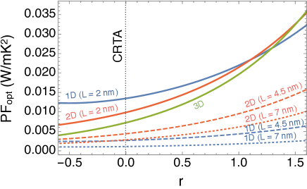
Next, we discuss some cases where may be enhanced significantly. Figure 1 shows as a function of the characteristic exponent for the 1D, 2D, and 3D systems, in which the values of range from to for various scattering processes Lundstrom (2000); Zhou et al. (2011). In these examples, we consider a typical semiconductor, n-type Si, at room temperature and high-doping concentrations on the order of cm-3. The thermal de Broglie wavelength and the carrier mobility are set to be and , respectively. We note that the scattering time assumed under the CRTA corresponds to , and thus Stradling and Wood (1970). As shown in Fig. 1, increases with increasing for all the 1D, 2D, and 3D systems. The effect of the characteristic exponent on the 3D system is stronger than that of the 1D and 2D systems. Based on Eq. (9) and Fig. 1, increases with decreasing corresponding to the confinement effect for the 1D and 2D systems. It is noted in Fig. 1 that in the 3D system does not depend on as shown in Eq. (9) with . However, the qualitative behaviour between and is not much affected by changing since and are independent of each other in Eq. (9).
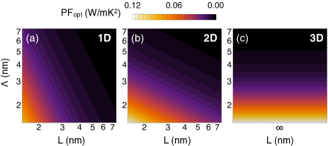
Figure 2 shows as a function of confinement length and thermal de Broglie wavelength for the 1D, 2D, and 3D systems. The mobility is set to be cm2/Vs for each system and the scattering rate may be proportional to the density of final states (DOS). By assuming proportionality of the scattering rate with respect to the DOS, we obtain , and for 1D, 2D, and 3D systems, respectively Zhou et al. (2011). Hereafter, we consider such different values for the different dimensions. The curves in Figs. 2(a) and (b) in particular show a and dependence of for 1D and 2D systems, respectively [cf. Eq. (9)]. These results are consistent with the Hicks-Dresselhaus model Hicks and Dresselhaus (1993a, b). In addition, in this Letter, we point out that it is important to consider the dependence of on . For an ideal electron gas under a trapping potential, the thermodynamic uncertainty principle may roughly be expressed as , where and are the pressure and volume of the system, respectively Farag Ali and Moussa (2014). The uncertainty principle ensures that when the confinement length is comparable with the thermal de Broglie wavelength, i.e., , the and cannot be treated as commuting observables. In this case, quantum effects play an important role in increasing for nanostructures. For a 1D system [Fig. 2(a)] starts to increase significantly when is much smaller than , while for the 2D system [Fig. 2(b)] starts to increase significantly when is comparable to . As for the 3D system [Fig. 2(c)], increases with decreasing for any values. Therefore, a nanostructure having both small and (while is also much smaller than its ) will be the most optimized structure to enhance .
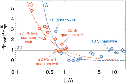
Now we can compare our model with various experimental data. In Fig. 3, we show as a function of for different dimensions (1D, 2D, and 3D systems) following Eq. (9). The values are scaled by the optimum power factor of a 3D system, . From Eq. (9), we see that the ratio merely depends on and . Hence, from various materials can be compared directly with the theoretical curves shown in Fig. 3. The experimental data in Fig. 3 are obtained from the values of 1D Bi nanowires Kim et al. (2015), 1D Si nanowires Hochbaum et al. (2008), 2D Si quantum wells Sun et al. (1999b), and two different experiments on 2D PbTe quantum wells labeled by PbTe–1 and PbTe–2 Harman et al. (1996); Hicks (1996). Here we use fixed parameters for the thermal de Broglie wavelength of each material: , , and . We also set some values for bulk systems: Kim et al. (2015), Weber and Gmelin (1991), Harman et al. (1996), and Hicks (1996), which are necessary to put all the experimental results into Fig. 3.
We find that the curves in Fig. 3 demonstrate a strong enhancement of in 1D and 2D systems when the ratio is smaller than one (). In contrast, if is larger than , the bulk 3D semiconductors may give a larger value than the lower dimensional semiconductors, as shown in Fig. 3 up to a limit of . We argue that such a condition is the main reason why an enhanced is not always observed in some materials although experimentalists have reduced the material dimensionality. For example, in the case of 1D Si nanowires, where we have , we can see that the experimental values in Fig. 3 are almost the same as the . The reason is that the diameters (supposed to represent ) of the 1D Si nanowires, which were about – in the previous experiments Boukai et al. (2008); Hochbaum et al. (2008), are still too large compared with . It might be difficult for experimentalists to obtain a condition of for the 1D Si nanowires. In the case of materials having larger , e.g., Bi with , the values of the 1D Bi nanowires can be enhanced at , which is already possible to achieve experimentally Kim et al. (2015). Furthermore, when , it is natural to expect that of 1D and 2D semiconductors resemble as shown by some experimental data in Fig. 3. It should be noted that, within the one-band model, we do not obtain a smooth transition of in Fig. 3 from the lower dimensional to the 3D characteristics for large because we neglect contributions coming from many other subbands responsible for the appearance of the 3D density of states Cornett and Rabin (2011).
So far, we have used the confinement length as an independent parameter in Eq. (9). It is actually possible to engineer the confinement length in the same material. For extremely thin films or nanowires, is expressed by two components as , where is the thickness of the material and is the size of the evanescent electron wavefunction beyond the surface boundary. Within the box of the electron wavefunction is delocalized, approximated by the linear combination of plane waves, while within the electron wavefunction is approximated by evanescent waves. For a single-layered material, e.g., a hexagonal boron nitride (h-BN) sheet, so that nm Lee et al. (2010). As for ultra-thick 1D nanowires or 2D thin films, we have , and thus the confinement length is mostly determined by the size of the material such as . Creating a 1D channel from a 2D material by applying negative gate voltages on two sides of the 2D material can be an example to engineer the confinement length Hirayama et al. (1989).
We already see that the thermal de Broglie wavelength depends on the temperature and the effective mass for the material. As given in Eq. (5), decreases ( or ) with increasing temperature or with increasing effective mass , which indicates that the [ in Eq. (9)] of nondegenerate semiconductors would be enhanced at higher or at larger (smaller ). This result is consistent with the experimental observations for the values of Si and PbTe, which are monotonically increasing as a function of temperature Hochbaum et al. (2008); Weber and Gmelin (1991); Sootsman et al. (2008). It should be noted that is not necessarily independent of and because the term may be altered by varying or by changing . For example, based on the fitting in Ref. Sajjad et al., 2009, the effective masses of 1D Si nanowires for within the interval of – nm could change from to , where is the free electron mass. Meanwhile, Ref. Green, 1990 reported that bulk 3D Si has an effective mass of about at room temperature. As a result, we estimate that the change of is roughly about – in this case. This fact might contribute to the small discrepancy between the values from our theory and those from experiments since we set as a fixed quantity upon variation of in 1D and 2D systems (see Fig. 3). For the 3D system, the theoretical values ( and ) are in good agreement with the experimental data ( Kim et al. (2015) and Weber and Gmelin (1991)).
In conclusion, we have shown that the largest power factor values might be obtained for low-dimensional systems by decreasing both the confinement length and the thermal de Broglie wavelength while keeping . Depending on the materials dimension, there is a different interplay between and to enhance the power factor. A simple analytical formula [Eq. (9)] based on the one-band model has been derived to describe the quantum effects on the in 1D, 2D, and 3D systems. We would suggest to experimentalists to be careful to check the trade-off between and in order to enhance for different dimensions of their semiconductors.
N.T.H. and A.R.T.N acknowledge the Interdepartmental Doctoral Degree Program for Multidimensional Materials Science Leaders in Tohoku University. R.S. acknowledges MEXT (Japan) Grants No. 25107005 and No. 25286005. M.S.D acknowledges support from NSF (USA) Grant No. DMR-1507806.
References
- Heremans et al. (2013) J. P. Heremans, M. S. Dresselhaus, L. E. Bell, and D. T. Morelli, Nat. Nanotechnol. 8, 471 (2013).
- Vining (2009) C. B. Vining, Nat. Mater. 8, 83 (2009).
- Majumdar (2004) A. Majumdar, Science 303, 777 (2004).
- Boukai et al. (2008) A. I. Boukai, Y. Bunimovich, J. Tahir-Kheli, J. Yu, W. A. Goddard III, and J. R. Heath, Nature 451, 168 (2008).
- Hochbaum et al. (2008) A. I. Hochbaum, R. Chen, R. D. Delgado, W. Liang, E. C. Garnett, M. Najarian, A. Majumdar, and P. Yang, Nature 451, 163 (2008).
- Liu et al. (2015) W. Liu, H. S. Kim, S. Chen, Q. Jie, B. Lv, M. Yao, Z. Ren, C. P. Opeil, S. Wilson, C. W. Chu, and Z. Ren, Proc. Natl. Acad. Sci. U.S.A. 112, 3269 (2015).
- Liu et al. (2016) W. Liu, H. S. Kim, Q. Jie, and Z. Ren, Scripta Mater. 111, 3 (2016).
- Hicks et al. (1996) L. D. Hicks, T. C. Harman, X. Sun, and M. S. Dresselhaus, Phys. Rev. B 53, R10493 (1996).
- Poudel et al. (2008) B. Poudel, Q. Hao, Y. Ma, Y. Lan, A. Minnich, B. Yu, X. Yan, D. Wang, A. Muto, D. Vashaee, X. Chen, J. Liu, M. S. Dresselhaus, G. Chen, and Z. Ren, Science 320, 634 (2008).
- Kim et al. (2015) J. Kim, S. Lee, Y. M. Brovman, P. Kim, and W. Lee, Nanoscale 7, 5053 (2015).
- Hicks and Dresselhaus (1993a) L. D. Hicks and M. S. Dresselhaus, Phys. Rev. B 47, 12727 (1993a).
- Hicks and Dresselhaus (1993b) L. D. Hicks and M. S. Dresselhaus, Phys. Rev. B 47, 16631 (1993b).
- Hung et al. (2015) N. T. Hung, A. R. T. Nugraha, E. H. Hasdeo, M. S. Dresselhaus, and R. Saito, Phys. Rev. B 92, 165426 (2015).
- Sun et al. (1999a) X. Sun, Z. Zhang, and M. S. Dresselhaus, App. Phys. Lett. 74, 4005 (1999a).
- Lundstrom (2000) M. Lundstrom, Fundamentals of Carrier Transport (Cambridge University Press, New York, 2000).
- Zhou et al. (2011) J. Zhou, R. Yang, G. Chen, and M. S. Dresselhaus, Phys. Rev. Lett. 107, 226601 (2011).
- (17) There is a difference in the exponent of the terms in Eq. (2) of this work and Eq. (B3) in Ref. 13, i.e., for this work and for Ref. 13. This is a consequence of the definition of adopted in this work and in Ref. 13.
- Silvera (1997) I. F. Silvera, Am. J. Phys. 65, 570 (1997).
- Stradling and Wood (1970) R. A. Stradling and R. A. Wood, J. Phys. C: Solid State Phys. 3, L94 (1970).
- Farag Ali and Moussa (2014) A. Farag Ali and M. Moussa, Adv. High Energy Phys. 2014, 629148 (2014).
- Sun et al. (1999b) X. Sun, S. B. Cronin, J. Liu, K. L. Wang, T. Koga, M. S. Dresselhaus, and G. Chen, in Proc. Int. Conf. Thermoelectrics (IEEE, 1999) pp. 652–655.
- Harman et al. (1996) T. C. Harman, D. L. Spears, and M. J. Manfra, J. Electron. Mater. 25, 1121 (1996).
- Hicks (1996) L. D. Hicks, Ph.D. thesis, MIT (1996).
- Weber and Gmelin (1991) L. Weber and E. Gmelin, Appl. Phys. A 53, 136 (1991).
- Cornett and Rabin (2011) J. E. Cornett and O. Rabin, Phys. Rev. B 84, 205410 (2011).
- Lee et al. (2010) C. Lee, Q. Li, W. Kalb, X. Z. Liu, H. Berger, R. W. Carpick, and J. Hone, Science 328, 76 (2010).
- Hirayama et al. (1989) Y. Hirayama, T. Saku, and Y. Horikoshi, Phys. Rev. B 39, 5535 (1989).
- Sootsman et al. (2008) J. R. Sootsman, H. Kong, C. Uher, J. J. D’Angelo, C.-I. Wu, T. P. Hogan, T. Caillat, and M. G. Kanatzidis, Angew. Chem. 120, 8746 (2008).
- Sajjad et al. (2009) R. N. Sajjad, K. Alam, and Q. D. M. Khosru, Semicond. Sci. Technol. 24, 045023 (2009).
- Green (1990) M. A. Green, J. Appl. Phys. 67, 2944 (1990).