Suspended graphene variable capacitor
The tuning of electrical circuit resonance with a variable capacitor, or varactor, finds wide application with the most important being wireless telecommunication. We demonstrate an electromechanical graphene varactor, a variable capacitor wherein the capacitance is tuned by voltage controlled deflection of a dense array of suspended graphene membranes. The low flexural rigidity of graphene monolayers is exploited to achieve low actuation voltage in an ultra-thin structure. Large arrays comprising thousands of suspensions were fabricated to give a tunable capacitance of over 10 pF/mm2, higher than that achieved by traditional micro-electromechanical system (MEMS) technologies. A capacitance tuning of 55% was achieved with a 10 V actuating voltage, exceeding that of conventional MEMS parallel plate capacitors. Capacitor behavior was investigated experimentally, and described by a simple theoretical model. Mechanical properties of the graphene membranes were measured independently using Atomic Force Microscopy (AFM). Increased graphene conductivity will enable the application of the compact graphene varactor to radio frequency systems.
Mechanically tuned variable capacitance has been an effective means to tune resonant circuits since the advent of radio Korda_patent . More compact varactors have since been developed in the form of an electrically tuned semiconductor junction capacitance Barnes_patent . Micro-electromechanical system (MEMS) implementations of varactors Larson_1999 combine the advantages of mechanical and semiconductor varactors in a single device architecture, including high electrical quality factor, high linearity, and the capacity for monolithic integration with silicon electronics Rebeiz_book . The canonical MEMS varactor is the parallel plate structure consisting of a conducting membrane suspended over a fixed plate, actuated by electrostatic attraction under an applied bias potential. While simple in structure, typical parallel plate varactors suffer high operating voltageYoung_1997 ; modeling_2009 and a limited capacitive tuning range. These limitations are typically overcome by complex mechanisms Baek_2015 , which increase both the size and actuation voltage.
Fundamentally, increasing the flexibility of a suspended element by reducing it’s thickness will reduce the actuation voltage of a parallel plate varator abdelghany_2012 . Monolayer graphene membranes achieve the ultimate limit with an inferred elastic stiffness of 390 N/m Bunch_2008 . In comparison a 15 nm thick Si3N4 membrane has an elastic stiffness of 6.3 kN/m. In addition to lower actuation voltage, graphene nano-electromecanical systems (NEMS) occupy less area than traditional MEMS counterpartschen_2013 , and can be easily integrated with integrated silicon electronics using standard transfer techniques Chen_2009 ; Huang_2015 . In the last decade, graphene NEMS have been widely investigated, including suspended graphene resonatorsBunch_2007 ; song_2012 ; weber_2014 , switchesmilaniana_2009 ; li_2012 ; li_2015 , and sensorsBunch_2008 . While the theoretical limits of suspended graphene varactors has been investigated abdelghany_2012 , large arrays of low spring constant suspensions has been plagued by low fabrication yield vanderZande_2010 . In this letter we report the fabrication and characterization of suspended graphene varactors. Each fabricated device is an array of over 1000 suspensions. The total tuneable capacitance of each varactor is .
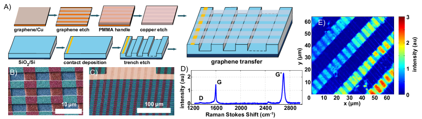
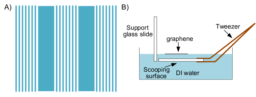
The varactors were fabricated by the process illustrated in Figure 1 A), consisting of three stages. The first stage is substrate preparation. Low resistivity Si wafers with 300 nm of thermal SiO2 were metallized and trenches were etched. The second stage is graphene growth and pre-patterning. Growth on Cu foils was performed by chemical vapor deposition, followed by photolithography and dry etching of graphene strips, and lastly a polymethylmethacrylate (PMMA) handle was used during a sacrificial Cu etch. In the final stage, graphene strips were transferred atop the trenches in a wet process with the suspensions released by critical point drying. Further processing details are provided in the supplementary information. A schematic of the fabricated device is illustrated in Figure 1A). Trenches of depth depth and length were fabricated, in arrays of at least 20 by 50 suspensions with an areal density of capacitance of . The active area of graphene suspensions constitutes of the total device area.
Figures 1B) and 1C) are false colour scanning electron micrographs of two different devices. Importantly, a layer of SiO2 at the bottom of the trench ensures that a single suspension collapse does not result in a short circuit. A critical parameter determining device yield is the aspect ratio of the trench length to the trench depth . Previously reported yields of suspended graphene arrays were for suspended strips over trenches with aspect ratios vanderZande_2010 , and for circular resonators over holes with aspect ratios less than 6.7barton_2011 . We have achieved a yield of for devices with aspect ratio .
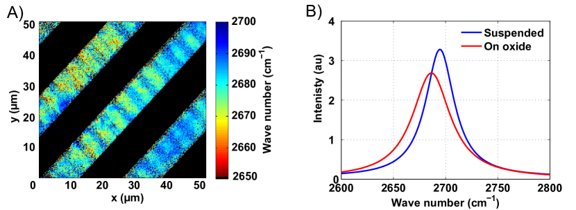
Raman spectroscopy was used to confirm the quality of the suspended graphene. Figure 2D) shows a representative Raman spectrum with a high intensity G’ peak () and a sharp G peak () indicative of predominantly monolayer graphene raman_book . The peak intensity ratio of the defect related D band ()) to the G peak is is 0.077, indicative of a low defect density raman_book . Furthermore, hyperspectral Raman imaging was used to independently confirm the continuity of graphene. Figure 1E) shows a spatial Raman map of the G’ peak intensity over a area. The peak intensity of supported graphene is greater than suspended graphene as the oxide thickness is optimal for Fabry-Pérot enhancement of optical intensity.
The varactor capacitance was measured in a vacuum probe station, as schematically shown in Figure 2A), including both the fixed parasitic capacitance and tuneable capacitance . A semiconductor parameter analyzer was used to measure the capacitance with an ac excitation of at a frequency while a dc bias voltage was swept to tune capacitance by electrostatic actuation of the suspended graphene membranes.
Figure 2B) shows the typical behavior of tuned capacitance versus bias for a typical graphene varactor among the five devices tested. At a bias voltage , the capacitance change is , exceeding the pull-in limit of a Hookean parallel plate varactor modeling_2009 . The measurement results agree well with a virtual displacement model imposing a balance of stretching, pre-tension and electrostatic forces on a graphene membrane,
| (1) |
where the membrane shape is approximated with a half-cosine, is the graphene Young modulus, is the pre-tension, is the graphene thickness, is the graphene Poisson raio, is a constant dependent on membrane aspect ratio vlassak_1992 , is the electrical length between Si substrate and graphene membrane, and is the graphene membrane deflection induced by applied bias . The capacitance is simply expressed in terms of the deflection abdelghany_2012 ,
| (2) |
Fitting the experimentally measured capacitance versus bias voltage, we extract a Young’s modulus and a pretension . Both and are lower than that reported in experiments with individual exfoliated graphene membranes Bunch_2007 .
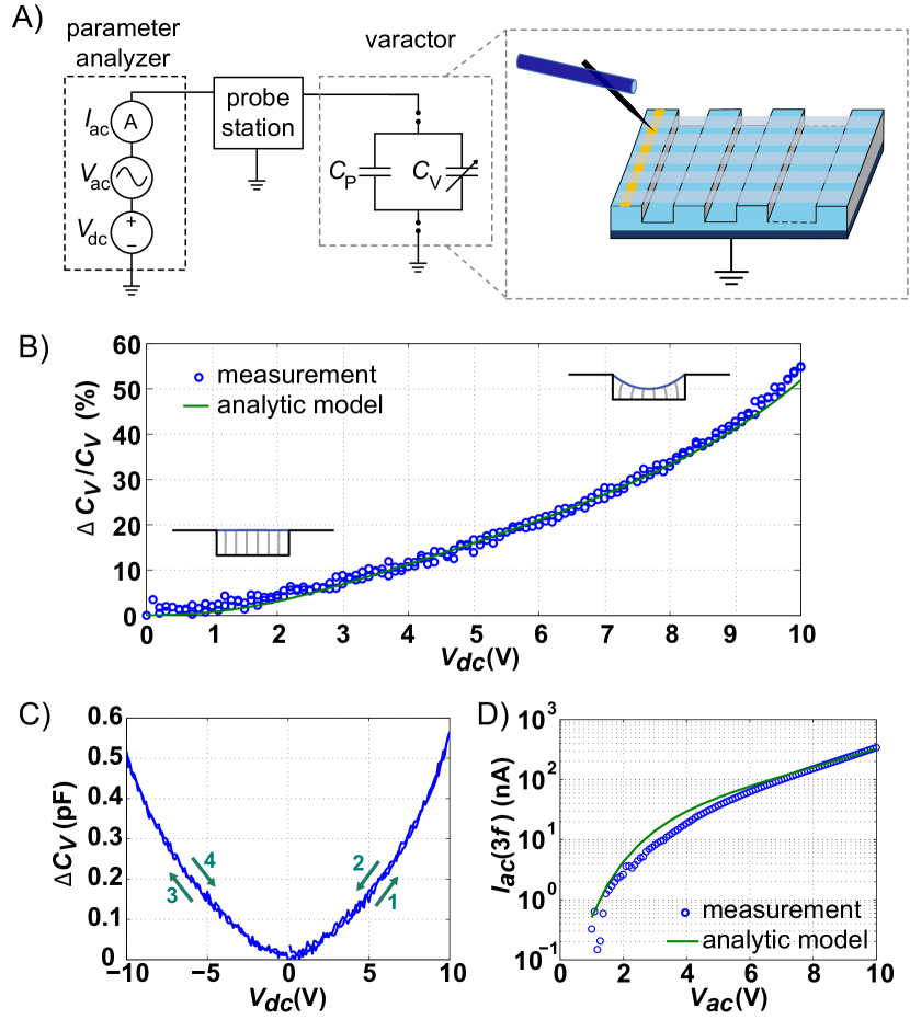
The ambivalent response of the varactor to the applied bias was measured, as shown in Figure 2C). Low hysteresis was observed for a 10 V swing of of either polarity. The non-linearity of the ambivalent response leads to odd harmonic generation in the resulting current spectrum, since the total ac current , where . We measured the third harmonic current with a lock-in amplifier tuned for ac excitation to at a frequency of . The measured versus is plotted in Figure 2D). A simple model for employing a quasi-static approximation for ignoring inertial effects leads to excellent agreement with measured results without any free fitting parameters. Notably, at the ratio , corresponding to less than third harmonic distortion in the varactor response.
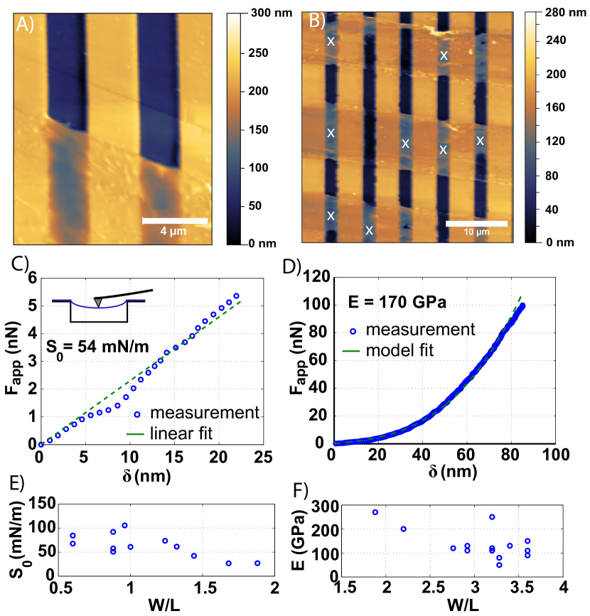
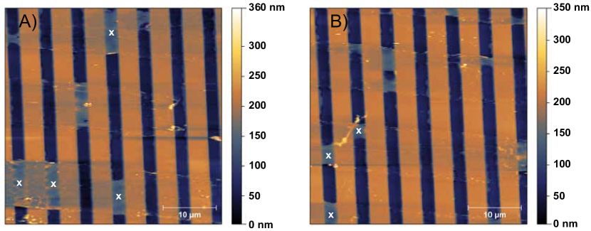
Atomic force microscopy (AFM) was used to independently verify the mechanical properties of individual suspended graphene membranes. Contact mode AFM images were first taken of the varactor, as shown in Figure 3A) and B). Force-deflection measurementsfrank_2007 were then conducted on 33 individual membranes, several of which are indicated in Figure 3B). A variety of membranes were selected, including several that underwent partial collapse following high voltage testing of varactor response. The deflection of a silicon cantilever with a calibrated spring constant () was measured as a function of the piezoelectric driven extension of the AFM, from which the force-displacement curve was inferred. Figure 3C) depicts a typical measurement of applied force versus graphene membrane displacement . For deflections , a linear fit determines the effective spring constant per Hooke’s law. Pre-tension dominates in the linear regime, and was estimated according to the beam approximation under a point load, . The pre-tension of 12 membranes are illustrated in Figure 3E) versus . Non-linearity in applied force versus deflection was observed at larger deflections due to graphene stretching, with an example illustrated in Figure 3D). The force versus deflection relation can be modelled for different geometries with a virtual displacement method (details provided in supplementary information), allowing a numerical fit to measurements and extraction of the Young’s modulus . The Young’s modulus of 14 membranes are illustrated in Figure 3F) versus , yielding a mean in good agreement with the value determined from capacitance measurements of the same varactor.
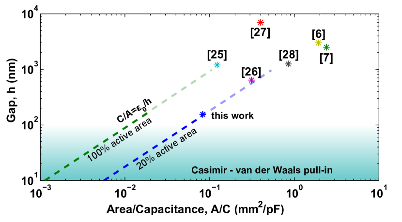
We finally consider a comparison of varactor height and area required to achieve , including the suspended graphene varactor and various state of the art MEMS varactors. The suspended graphene varactor offers the highest capacitance density in the smallest vertical space. Improving the active area occupation of total device area beyond will further increase the capacitance density of the graphene varactor. At active area occupation, the areal capacitance density reaches the limit imposed by the permittivity of free space, . The ultimate limit to the achievable areal capacitance density of suspended graphene will be determined by the minimum trench depth that can be sustained without spontaneous pull-in by Casimir-van der Waals forces. The criterion for spontaneous pull-in by Casimir-van der Waals forcesserry_1998 in the ideal conductor limit is with . For a trench aspect ratio , a minimum trench height of and maximum capacitance density of can be theoretically achieved.
In conclusion, we have demonstrated large area suspended graphene varactors, reaching a tuning range with a 10 V actuation voltage, a high device yield and an areal capacitance density of . Further reduction in pull-in voltage may be achieved by increasing the trench aspect ratio , but avoiding spontaneous pull-in by Casmir-van der Waal forces will require increased height , and thus reduced areal capacitance. The application of graphene varactors to radio frequency circuits requires the challenge of monolithic integration to be addressed through more advanced fabrication processes.
References
- (1) Korda, D. Elektrischer kondensator mit durch lagenänderung der platten veränderlicher capacität, Kaiserliches Patentamt 72447 filed 8 June 1892, and issued 13 December 1893.
- (2) Barnes, S. H., Oaks, J. E. & Mann, J. E. Voltage sensitive semiconductor capacitor, US Patent 2,989,671 filed 23 May 1958, and issued 20 June 1961.
- (3) Larson, L. E. Microwave mems technology for next-generation wireless communications. In Microwave Symposium Digest, 1999 IEEE MTT-S International, vol. 3, 1073–1076 (1999).
- (4) Rebeiz, G. M. RF MEMS: Theory, Design, and Technology (John Wiley & Sons, 2004).
- (5) Young, D. J. & Boser, B. E. A micromachine-based rf low-noise voltage-controlled oscillator. In Custom Integrated Circuits Conference, 1997., Proceedings of the IEEE 1997, 431–434 (1997).
- (6) Zhang, B. & Fang, D. Mech Mach Theory 44, 647–655 (2009).
- (7) Baek, D.-H. et al. Widely tunable variable capacitor with switching and latching mechanisms. Electron Device Letters, IEEE 36, 186–188 (2015).
- (8) AbdelGhany, M., Ledwosinska, E. & Szkopek, T. Theory of the suspended graphene varactor. Applied Physics Letters 101, – (2012).
- (9) Bunch, J. S. et al. Impermeable atomic membranes from graphene sheets. Nano Letters 8, 2458–2462 (2008).
- (10) Chen, C. et al. Graphene mechanical oscillators with tunable frequency. Nature Nanotechnology 8, 923–927 (2013).
- (11) Chen, X. et al. High-speed graphene interconnects monolithically integrated with cmos ring oscillators operating at 1.3ghz. In Electron Devices Meeting (IEDM), 2009 IEEE International, 1–4 (2009).
- (12) Huang, L. et al. Graphene/si cmos hybrid hall integrated circuits. Scientific Reports 4, 5548 (2014).
- (13) Bunch, J. S. et al. Electromechanical resonators from graphene sheets. Science 315, 490–493 (2007).
- (14) Song, X. et al. Stamp transferred suspended graphene mechanical resonators for radio frequency electrical readout. Nano Letters 12, 198–202 (2012).
- (15) Weber, P., Guttinger, J., Tsioutsios, I., Chang, D. E. & Bachtold, A. Coupling graphene mechanical resonators to superconducting microwave cavities. Nano Letters 14, 2854–2860 (2014).
- (16) Milaninia, K. M., Baldo, M. A., Reina, A. & Kong, J. All graphene electromechanical switch fabricated by chemical vapor deposition. Applied Physics Letters 95 (2009).
- (17) Li, P., You, Z. & Cui, T. Graphene cantilever beams for nano switches. Applied Physics Letters 101, 093111 –093111–5 (2012).
- (18) Li, P. & Cui, T. Rf nano switch based on single crystalline graphene. In Solid-State Sensors, Actuators and Microsystems (TRANSDUCERS), 2015 Transducers - 2015 18th International Conference on, 307–310 (2015).
- (19) van der Zande, A. M. et al. Large-scale arrays of single-layer graphene resonators. Nano Letters 10, 4869–4873 (2010).
- (20) Barton, R. A. et al. High, size-dependent quality factor in an array of graphene mechanical resonators. Nano Letters 11, 1232–1236 (2011).
- (21) Jorio, A., Saito, R., Dresselhaus, M. S. & Dresselhaus, G. Raman Spectroscopy in Graphene Related Systems (WILEY-VCH, 2011).
- (22) Vlassak, J. & Nix, W. A new bulge test technique for the determination of young’s modulus and poisson’s ratio of thin films. Journal of Materials Research 7, 3242–3249 (1992).
- (23) Frank, I. W., Tanenbaum, D. M., van der Zande, A. M. & McEuen, P. L. Mechanical properties of suspended graphene sheets. Journal of Vacuum Science & Technology B 25, 2558–2561 (2007).
- (24) Serry, F. M., Walliser, D. & Maclay, G. J. The role of the casimir effect in the static deflection and stiction of membrane strips in microelectromechanical systems (mems). Journal of Applied Physics 84, 2501–2506 (1998).
- (25) Elshurafa, A., Salama, K. & Ho, P. Modeling and fabrication of an rf mems variable capacitor with a fractal geometry. In Circuits and Systems (ISCAS), 2013 IEEE International Symposium on, 2711–2714 (2013).
- (26) Bakri-Kassem, M., Fouladi, S. & Mansour, R. Novel high-q mems curled-plate variable capacitors fabricated in 0.35-um cmos technology. Microwave Theory and Techniques, IEEE Transactions on 56, 530–541 (2008).
- (27) Achenbach, S., Haluzan, D., Klymyshyn, D., Börner, M. & Mohr, J. Large tuning ratio high aspect ratio variable capacitors using leveraged bending. Microsystem Technologies 20, 1807–1813 (2014).
- (28) Han, C.-H., Choi, D.-H. & Yoon, J.-B. Parallel-plate mems variable capacitor with superior linearity and large tuning ratio using a levering structure. Microelectromechanical Systems, Journal of 20, 1345–1354 (2011).
Appendix A Supplementary information for Suspended graphene variable capacitor
M. AbdelGhany∗, F. Mahvash, M. Mukhopadhyay, A. Favron, R. Martel, M. Siaj, and T. Szkopek†
A.1 Fabrication Process
A.1.1 Substrate preparation
The devices were fabricated on a low resistivity silicon wafer with nm of thermal oxide on both sides. The oxide was completely removed from one side to allow access to the silicon. It was removed by wet itching in a 10:1 diluted hydrofluoric acid for 20 minutes, while covering the other side of the wafer with photo-resist and protective tape to preserve the oxide on this side. Afterwards metal contacts were deposited on the front side using lift-off process. Photolithography was used for lift-off, we spun 700 nm of LOR 5B lift-off resist under 1.4 of S1813 positive resist to create an undercut for lift-off. The metal was deposited using electron beam evaporation. Metal contacts consisted of 100 nm gold over 10 nm titanium, the titanium improved the adhesion of the contacts. The lift-off was done by putting the wafer in Remover 1165 at with sonication for 20 minutes. Afterwards the wafer was transferred to a fresh beaker of Remover 1165 and left for another 10 minutes at , then the wafer was rinsed in Isopropyl alcohol (IPA) and deionized (DI) water for five minutes each. Oxygen plasma was used to get rid of all resist residue.
The trenches were etched using photolithography and reactive ion etching (RIE). The etch rate was calibrated for narrow trenches as it decreases with trench width. Atomic force microscopy (AFM) was used to accurately measure the trench depth and calibrate the etch rate. After the desirable depth was achieved, the resist was removed using the same method described above.
A.1.2 Graphene growth and pre-patterning
We used large area graphene grown by chemical vapor deposition (CVD). We grew single layer graphene on both sides of a 25 sheet of copper foil. Before transfer the graphene on the desired side was pre-patterned using photolithography and RIE to create graphene strips to facilitate suspension as well as alignment marks to help transfer the graphene strips orthogonal to the trenches. Figure S1A) shows the graphene pattern used. The continuous pieces acted as alignment marks, as there is a clear difference in transparency between them and the regions with narrow strips.
The graphene was etched using oxygen plasma RIE with 100 W RF power, 200 mT pressure, and a gas flow of 40 scc. After the patterning, the copper pieces were left in acetone for five minutes to remove the photoresist, then rinsed in IPA and DI water for five minutes each.
A.1.3 Graphene transfer
To prepare for transfer, The patterned graphene was covered with 300 nm of PMMA 950 A4 polymer handle for mechanical support. The polymer was then baked at for three minutes. The copper was etched in a 0.1 molar solution of ammonium per-sulphate , after minutes of etching the samples were removed and the back side of the copper foil was sprayed with DI water to remove the graphene on that side. After the copper etching was done (in hours) the graphene with the polymer handle was left floating over the . It was then scooped from the etchant and transferred to a beaker of DI water and left for five minutes. After that the graphene was transferred to a fresh beaker of DI water to get rid of all residue. Finally the graphene is scooped on the prepared substrate and left to dry for hours. Figure S1B) shows how the graphene was scooped out of liquids.
After the sample dried, the PMMA was removed by putting the sample in acetone for four hours, then transferring it to a fresh beaker of acetone for 30 minutes. The sample was then transferred to a beaker of IPA and left for five minutes. It was transferred to a fresh beaker of IPA two or three more times to get rid of all acetone residue. While transferring the graphene the sample had to be kept horizontal so that it would be covered in liquid at all time, this was crucial to prevent the collapse of suspended strips. The sample was then transferred in the same manner to the chamber of an ’Automegasamdri®-915B, Series B’ critical point dryer. For our samples, only one fourth of the chamber was use. It was filled with enough IPA to cover the sample. The purge time was adjusted to 20 minutes. After drying, the graphene strips were cut around each individual device to separate the devices from each other. A profilometer stylus was used for cutting the graphene.
A.2 Raman verification
A Raman image was taken for the graphene varactor to verify the continuity of the graphene over the whole device. The image was taken using hyper spectral imaging system (Photon Etc.) with pump wavelength of 532 nm. A map of the wavenumber shift of the G’ peak at each spatial point is shown in figure S2 A). The map illustrates that graphene strips are continuous over the trenches, with a different wavenumber shift of the G’ peak between the suspended graphene and that supported on oxide. There is a blue shift in the suspended graphene. This shift was verified using spot Raman measurements, figure S2 B) depicts the Lorentzian fit of G’ peaks of two spots on the same strip, one suspended and the other supported. The spot measurement shows a shift of 8 between the peaks which agrees with the hyperspectral map.
A.3 Calibration of test equipment
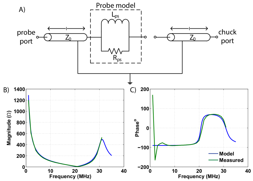
The electrical measurements were done in a Janis Research ST-500 probe station. The graphene was contacted by landing a probe on the metal pad, while the bulk of the silicon was fixed to the probe station chuck and acted as the other electrode. To obtain accurate results the probe station frequency response was extracted. A network analyser was used to find the S-parameters of the probe station in open-circuit and short circuit. A circuit model was extracted from these measurements. Figure S3 A) depicts the extracted circuit model, while figure S3 parts B) and C) compare the input impedance of the extracted model to that measured using the network analyser in the short-circuit case.
The non-linear current response of the varactor was measured using Zurich Instruments HF2 lock-in amplifier with the HF2TA current amplifier. To account for the current amplifier effects, its frequency response was measured using a known load.
A.4 Theoretical calculation of varactor non-linearity
Due to the complexity of the system no closed form relation could be reached for the non-linear components of the current, however numerical solutions were obtained. To facilitate the construction of a numerical model predicting the non-linearity of the varactor, it was assumed that the deflection of the suspended membranes it comprises is adiabatically invariant therefore the system is at equilibrium at all points in time and effects of damping can be ignored. This way the system was solved at each time point independently. This assumption is valid for frequencies much lower than the membrane resonant frequency, thus we limited the non-linearity study to frequencies below 1 MHz while the expected resonant frequency of the membrane is 73 MHz. Figure S4A) shows the deflection at the centre of the suspended graphene membrane and the resulting current versus time due to applied AC voltage.
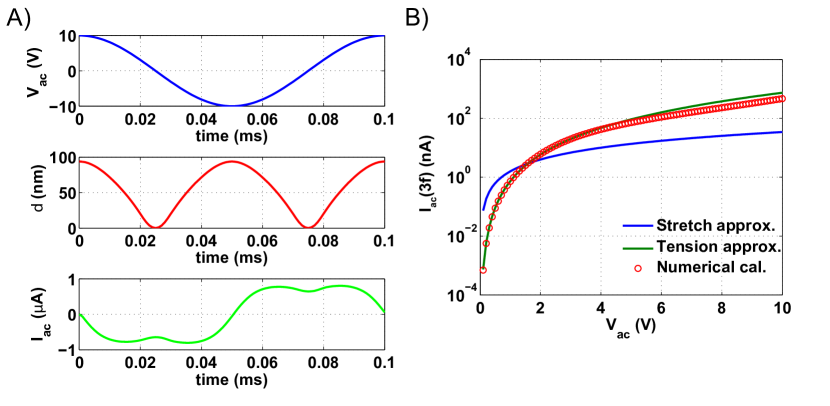
For deflections much smaller than the trench depth , a closed form relation can reached. At these deflections the membrane behavior is dominated by either the stretching restoring mechanism or the residual tension restoring mechanism. In the first case the additional current due to membrane deflection is given by equation S1, while in the case of pretension dominated behavior, the additional current is given by equation S2. Figure S4B) shows how the two cases compares with our numerical calculations. The pretension approximation agrees with the numerical calculations for low voltage as our devices behavior is dominated by pretension at small deflection values.
| (S1) |
| (S2) |
where is the initial capacitance, is a constant depending on material properties (Young’s modulus and Poisson’s ratio), is a constant depending on the membrane shape and residual tension, and and are the capacitor length and height respectively.
A.5 Force displacement measurement
The methods used in this experiment are similar to those used in references frank_2007 ; Lee_2008 ; Whittaker_2006 . The force displacement data was acquired using an Asylum MFP3D AFM. Bruker MLCT-F tips were used for the measurements, the cantilevers carrying the tips had spring constants between 0.9 N/m and 0.95 N/m. The average width of the suspended strips was 9 with 90% of the strips between 8 and 9.5 . Thirty three suspension with widths between 1.5 and 9 were probed. The device was imaged before starting the experiment to accurately choose the indentation position. The geometric centre of each suspension was chosen for probing as indicated by the white marks in figure S5. Suspensions with no defects were chosen.
The microscope was kept scanning for 20 minutes before the indentation to minimize the x-y drift. Each suspension was then tested with maximum force of 10 nN. The test was repeated twice to account for slippage and breakage of the membrane. Figure S6A) shows the raw data from a suspension where the first indentation did not cause damage thus the two sets of data agree, while figure S6B) shows the data from a suspension where the first indentation caused some damage therefore the second set of data is different. Suspensions that showed signs of damage were excluded from the experiment. Half of the suspensions were then tested with maximum force of 150 nN to probe the non-linear membrane (stretching) behavior, from which Young’s modulus can be extracted. The experiment recorded the piezo displacement , the tip deflection , and the applied force . The graphene deflection was extracted by subtracting the tip deflection from the piezo displacementfrank_2007 ; Lee_2008 . It was necessary to determine the point at which tip deflection is zero to obtain accurate results.
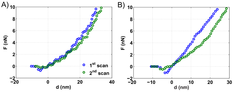
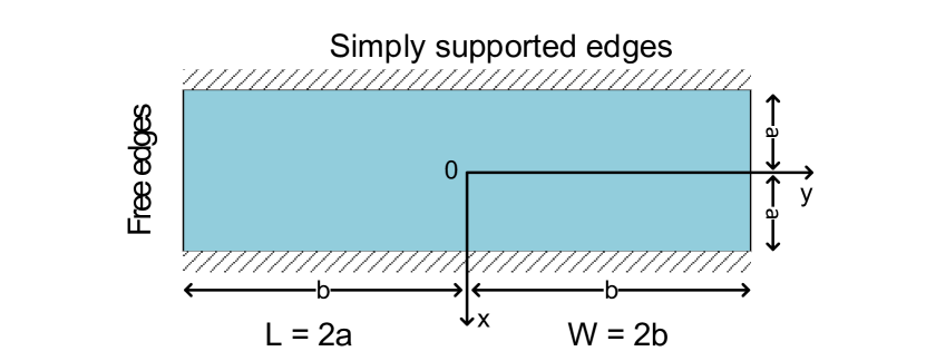
The measured force deflection relation was linear up to , which suggested the membranes were dominated by pretension. For deflections higher than 10 nm, the relation was non-linear as the membranes transitioned to the stretching behavior regime. There is no exact closed form model describing the non-linear (stretching) suspended rectangular membranes loaded at the centre due to the complexity of the geometry and the load, exact solutions can be only found for circular membranes under certain condition due to the axisymmetry of their geometryKomaragiri_2005 ; Zhang_2014 . Therefore to fit the acquired data an approximate model was developed. The model was developed for rectangles with width larger than twice their length. This geometry is the most representative of our suspended strips, also the width of the rectangles allows us to neglect the deflection of the free edges. Thus all edges were assumed to be simply supported and immovable. A half cosine deflection profile was assumed. Figure S7 illustrates the geometry of the membranes under consideration.
The virtual displacement method described in reference Timoshenko was used to find an approximate force deflection relation in the non-linear membrane domain (large deflection). After each derivation step the result was compared to the values found in the reference for the square limit. The approximate expressions for the displacements are:
where , , are the displacements in , , and directions respectively. is the deflection at the centre of membrane, and and are the maximum displacements in and directions respectively . The final force deflection relation is given by:
| (S3) |
where F is the applied force, E is Young’s modulus, and t is the thickness of the membrane. This relation was calculated for a Poisson’s ratio of 0.141. For a square, the force deflection relation is:
| (S4) |
when this relation is adjusted for a uniform load and a Poisson’s ratio of 0.25 the relation becomes , which agrees with reference Timoshenko .
References
- (1) Whittaker, J. D., Minot, E. D., Tanenbaum, D. M., McEuen, P. L. & Davis, R. C. Measurement of the adhesion force between carbon nanotubes and a silicon dioxide substrate. Nano Letters 6, 953–957 (2006).
- (2) Lee, C., Wei, X., Kysar, J. W. & Hone, J. Measurement of the elastic properties and intrinsic strength of monolayer graphene. Science 321, 385–388 (2008).
- (3) Frank, I. W., Tanenbaum, D. M., van der Zande, A. M. & McEuen, P. L. Mechanical properties of suspended graphene sheets. Journal of Vacuum Science & Technology B 25, 2558–2561 (2007).
- (4) Zhang, L., Wang, J. & Zhou, Y.-H. Wavelet solution for large deflection bending problems of thin rectangular plates. Archive of Applied Mechanics 85, 355–365 (2014).
- (5) U. Komaragiri, M. R. B. & Simmonds, J. G. The mechanical response of freestanding circular elastic films under point and pressure loads. Journal of Applied Mechanics 72(2), 203–212 (2005).
- (6) Timoshenko, S. & Woinowsky-Krieger, S. Theory of plates and shells (McGraw-Hill Book Company, 1959).