A multiplexer for the ac/dc characterization of TES based bolometers and microcalorimeters.
Abstract
At SRON we are developing the Frequency Domain Multiplexing (FDM) for the read-out of the TES-based detector array for the future infrared and X-ray space mission. We describe the performances of a multiplexer designed to increase the experimental throughput in the characterisation of ultra-low noise equivalent power (NEP) TES bolometers and high energy resolving power X-ray microcalorimeters arrays under ac and dc bias. We discuss the results obtained using the TiAu TES bolometers array fabricated at SRON with measured dark NEP below and saturation power of several fW.
keywords:
FDM. cryogenic detector,TES, infrared bolometers, SQUID, x-ray microcalorimeter1 INTRODUCTION
We developed a Frequency Domain Multiplexer (FDM) in order to increase the experimental throughput in the characterisation of TES-based X-ray microcalorimeters and bolometer array under ac bias at frequency higher than 1 MHz. To simultaneously measure a large number of pixels a baseband feedback scheme [1] is required. However, to perform a single pixel characterisation, each ac channel can be read-out sequentially in time. In this way the SQUID amplifier dynamic range is less critical and the read-out of a single low-G bolometers, generally operating at TES rms current values lower than , can be done in open loop. The X-ray TES microcalorimeters operate at larger current then the bolometers. It that case baseband feedback will be used.
Another reason to develop a new FDM set-up was to understand the energy resolution degradation observed with X-ray microcalorimeters under AC bias [2] So far the ac bias experiments where carried on at frequencies below 700kHz, using sub-optimal circuit elements such as high-inductance SQUID amplifiers with strong coupling between feedback and input coil, low-Q discrete LC resonators and large stray inductance and resistance connections. It has been shown that operating the TES under ac bias at too low a frequency can lead to a degradation of the energy resolution [3]. Only recently high-Q lithographic, superconducting LC filters[4], tuned to frequencies between 2 to 5MHz, and high dynamic range, low input inductance SQUID became available for the FDM read-out at MHz. This novel technology has been implemented in the FDM set-up.
Moreover, the experiments set-up used so far suffered from a poor magnetic shielding. We greatly improve the magnetic field shielding of our single pixel test bed. The optimal shielding design and the accurate selection of non-magnetic components guarantees an uniform and low (Tesla) magnetic field environment at the detector stage.
2 EXPERIMENTAL SET-UP
The multiplexers described below was developed to be used both with ultra-low noise equivalent power (NEP) TES bolometers and with high energy resolving power x-ray microcalorimeters. The former requires very low parasitic power loading (), which is achieved by means of light blocking filters in the signal loom feedthrought and a light-tight assembly. The x-ray microcalorimeters are very sensitive to magnetic fields and their performance is optimal at static field lower than ). Special care has been taken to design the magnetic shielding and to improve the uniformity of the applied magnetic field across the array. The FDM multiplexer consists of a low magnetic impurity copper bracket mounting on top the SQUID array, the LC filters and the TES array chips and a printed circuit board for the electrical connection. One thermometer and one heater are glued at the bottom of the copper plate for the read-out and stabilisation of the temperature.
The TES arrays chip fits into a superconducting Helmholtz coil fixed at one end of the bracket. The coil is used to generate an uniform perpendicular magnetic field over the whole pixels array. A schematic drawing and a picture of the set up is shown in Fig. 1.
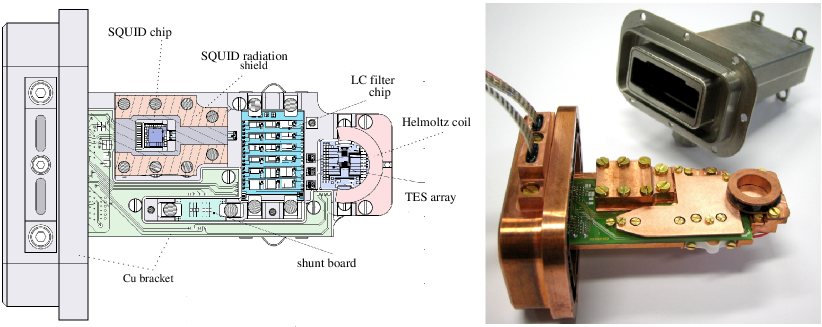
The shielding of the external magnetic field was achieved by fitting the bracket into a Nb can wrapped by few layers of metallic glass tape. The matching of the Nb can with the bracket lid was designed such that it forms a labyrinth, filled with carbon loaded epoxy on the copper lid side. In this configuration the Nb can provides both the required magnetic and stray light shielding.
The electrical connections from the cold stage of the cooler to the SQUID array and TES bias circuit elements are achieved by means of two superconducting looms fed through a narrow 10 mm long channel filled with carbon loaded epoxy. The circuitry PC-board currently allows to read-out 18 pixels under ac bias in a FDM configuration and 2 pixels under dc or ac bias with the SQUID amplifier located outside the Nb can.
For the FDM read-out we use a low noise two-stage PTB SQUID array current sensor with on chip linearization [7], low input inductance () and low power dissipation () [8]. The SQUID amplifier chip is placed in a radiation shielding cavity whose inner side is coated with a 2 mm thick radiation absorber made from carbon loaded epoxy with mixed SiC grains with size ranging from to 1 mm [9, 10]. This precaution was taken to minimise possible loading of the bolometers due to Josephson radiation, typically in the range of 4-8 GHz, emitted by the SQUID junctions. The SQUID chip is thermally coupled to the bracket by means of several Au bonding. The electrical connection from the SQUID chip to the LC filters is done by means of Nb strip lines on a 20 mm long interconnection chip. These lines act as a low-pass filter with a calculated roll-off around 500 MHz. We operate the SQUID in open loop. The output signal is amplified by a 20 MHz bandwidth, low input voltage noise, commercial electronics (Magnicon GmbH).
The TES array chip is connected via a superconducting interconnection chip to the lithografic high-Q LC resonators arrays developed at SRON [4]. The nominal inductance of the coil used in each filter is , while the capacitances C are designed such that the frequencies are spread at a constant interval of about 200kHz in the range from 2 to 5 MHz. The LC filter chip used had 18 filters of which 14 were properly functioning.
3 FDM READ-OUT CHARACTERISATION
We evaluated the performance of the FDM read-out by measuring the SQUID input current noise and dynamic range, the quality factor of the LC filters and the uniformity and goodness of the magnetic shielding.
3.1 SQUID amplifier and LC filters test
In Fig. 2 we show the SQUID input current spectral density during nominal operation of the multiplexer.
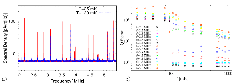
For the measurements described here we connected 8 low-G bolometers, with a normal resistance and , to 8 LC filters with resonance frequencies of 2.2, 2.4, 2.6, 2.8, 3.4, 3.6, 4.2 and 4.6 MHz respectively. The other filters were superconducting shorted using Al bonding. At temperature we measured a SQUID input current noise of (with ) over the whole interesting frequency range from 2 to 5 MHz, as expected for this particular SQUID chip. All the resonators had a Q factor larger than at . The SQUID operates in a linear regime for peak-peak input currents lower than corresponding to a dynamic range of .
3.2 Magnetic shielding
In order to test the quality of the magnetic shielding we measured the current response of several TES pixels, distributed over a surface of in diameter, as a function of the magnetic field applied perpendicularly to the TES. The results are shown in Fig. 3. For each measured pixel the response is symmetric around the applied magnetic field . This value is an estimation of the residual magnetic field perpendicular to the TES.
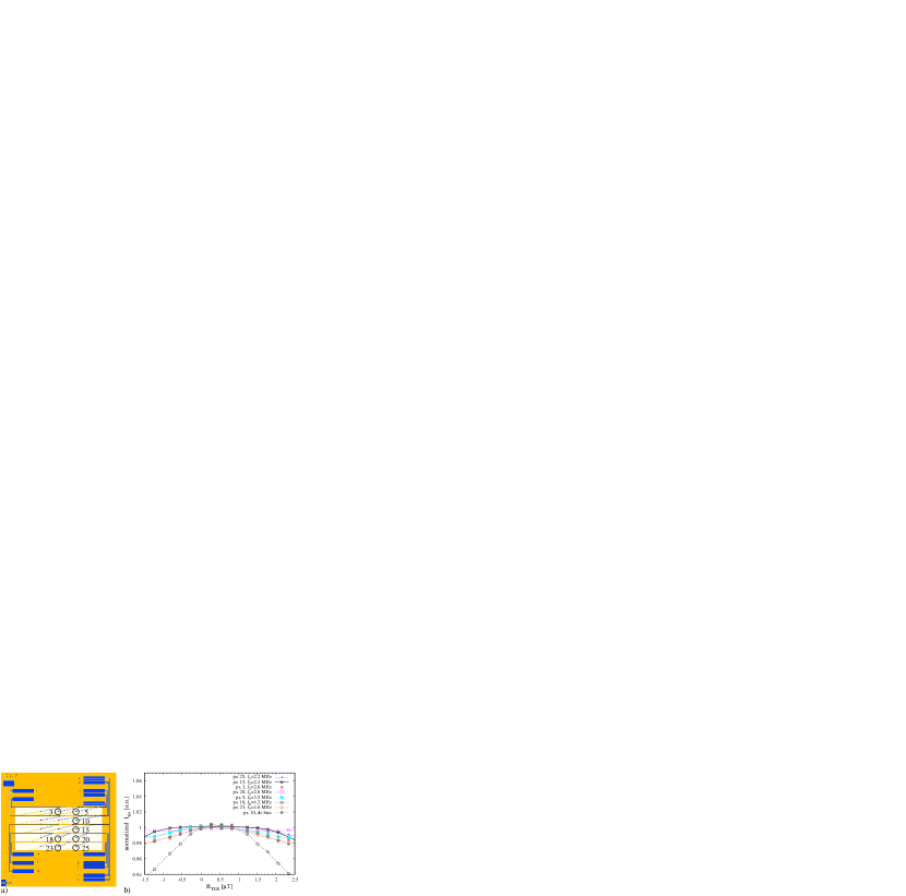
From the graphs we estimate that the B-field shielding and the B-field bias is uniform within , In more than 6 cryogenic runs the measured residual magnetic field has always been better than .
4 SINGEL PIXEL CHARACTERIZATION WITH THE FDM SET-UP
In the following session we present the results of a single pixel characterisation using the readout channel at 2.4MHz.
The device under test is a low-G bolometer based on a Ti/Au (16/60 nm) bilayer, deposited on thick suspended SiN membrane. The TES area is . It has a critical temperature of , a normal state resistance of , a measured pW/K and a calculated NEP of . An 8 nm thick Ta absorber with an area of is deposited close to the TES. The absorber and the TES are sitting on a SiN island. Fig. 4 shows a picture of the device.
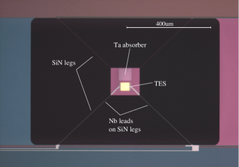 |
There are 4 SiN cross-shaped supporting legs that are wide and long. The electrical contact to the bolometer is realized by 90 nm thick Nb wiring on the top of SiN legs. The sensor was previously characterised under dc bias in the set-up described in [5, 6] and showed a power plateau of and a dark NEP of at 30 mK. The pixel is fabricated on a test chip with 4 other pixels.
4.1 Current-voltage and power-voltage characteristics
In Fig. 5 we show the TES current-to-voltage and power-to-voltage characteristics measured both under ac and dc bias at a bath temperature of T=30 mK and at zero perpendicular magnetic field.
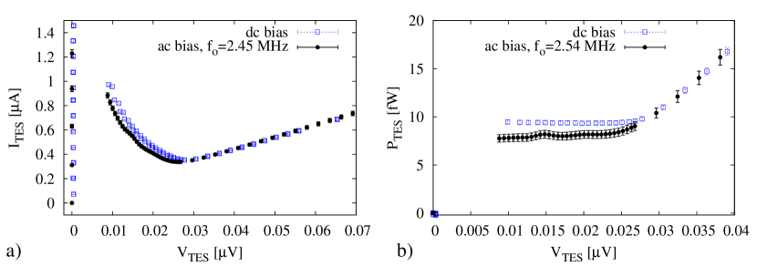
Under ac bias the saturation power is , which is about 2 fW lower than the power observed in the dc bias measurement set-up.
The SQUID amplifier mounted inside the light-tight box in the FDM set-up is a possible source of power loading. The power dissipated in the SQUID at its optimal working point is about 15 nW. In order to quantify the amount of power leaking from the SQUID to the bolometer array we measured the power-voltage characteristic of another pixel in the array using an auxiliary ac read-out system. In this case the TES signal is measured by a SQUID array hosted in a module mounted externally to the light-tight box. When switching the FDM SQUID array on and off we observed a difference of about 0.5 fW in the pixel saturation power, which is not sufficient to fully explain the parasitic loading at 30mK.
At bath temperatures the saturation power measured under ac and dc bias was the same within the measurement uncertainties. The latter observation excludes the presence of an electrical loading since the read-out conditions are identical at all bath temperatures. A possible explanation for the lower power plateaux measured at in the FDM set-up could be a bad thermalization of its circuit components. A difference of about 15 mK between the measured temperature of the copper bracket and the real temperature of the bolometer array Si chip is sufficient to explain the discrepancies observed.
We believe that this issue can be solved with minor improvement of the experimental setup and does not put any fundamental constrain in the performance of a low-G bolometer under ac bias.
4.2 Noise measurements
Fig. 6 shows the dark NEP spectra at several bias points in the transition for a bath temperature of 30 mK.
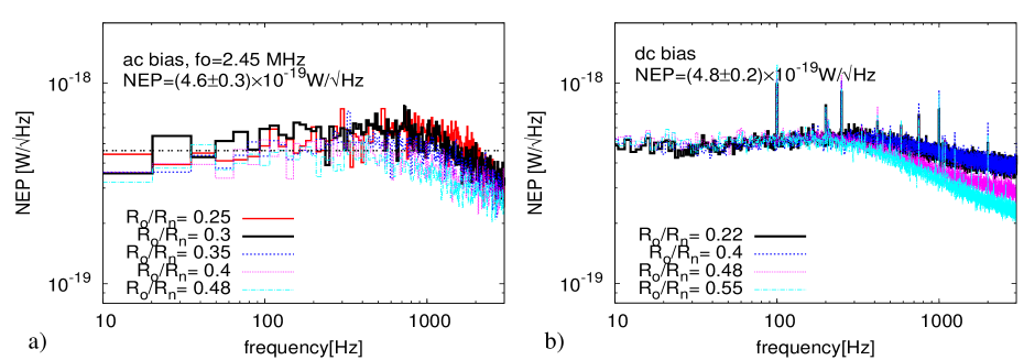 |
Both the results obtained under ac and dc bias are shown. The dark NEP was calculated by dividing the current noise by the responsivity at low frequency. which can be approximated by , where is the effective bias current, is the TES resistance and is the Thevenin impedance in the bias circuit as derived from the calibration of the I-V curves. The measured dark NEP at low frequency at all working points in the transition was about and respectively for the ac and dc bias case.
5 CONCLUSION
We fabricated and tested an FDM set-up for the single pixel characterisation of TES based bolometer and microcalorimeters under ac bias in the MHz frequency range. The set-up is designed to read out 18 pixels under ac bias and 2 pixels under ac or dc bias.
We validate the performance of the ac bias read-out by characterising the SQUID amplifier, the lithographic high-Q LC filters and the magnetic shielding at . The SQUID amplifier has an input current noise of and a dynamic range of over the whole interesting frequency range from 2 to 5 MHz. All the measured superconducting LC resonators has a Q-factor larger than at . We measured a static magnetic field of the order of inside the Nb shield at the array location and perpendicular to the pixels. The residual field is uniform within over an area of and found to be reproducible in more than six cryogenic runs.
We fully characterised a low-G device at an ac bias frequency of 2.5 MHz. The TES pixel was previously measured under dc bias in a different cryogenic set-up. The pixel showed comparable noise feature when operating under ac and dc bias. A dark NEP of was observed at 30 mK with the ac bias readout. The detected saturation power was under ac bias, which was about 2 fW lower than the power observed in the dc bias measurement set-up. We believe this was due to a bad thermalization of the LC filter and bolometer array chips and that this issue can be solved with minor improvement of the experimental setup. From the measurements reported here we therefore conclude that the behaviour of the low-G bolometers operating under dc bias and ac bias at a frequency of 2.4MHz is equal.
A similar FDM set-up is currently being assembled to perform single pixel characterisation of TES-based X-ray microcalorimeter array.
Acknowledgements.
We thank Marcel van Litsenburg, Lou Verhagen and Robert Huiting for their precious technical help.References
- [1] R. den Hartog, M. Audley, J. Beyer, D. Boersma, M. Bruijn, L. Gottardi, H. Hoevers, R. Hou, G. Keizer, P. Khosropanah, M. Kiviranta, P. de Korte, J. van der Kuur, B.-J. van Leeuwen, A. Nieuwenhuizen, and P. van Winden, “Low-noise readout of TES detectors with baseband feedback frequency domain multiplexing,” Journal of Low Temperature Physics 167, pp. 652–657, 2012.
- [2] L. Gottardi, J. Adams, C. Bailey, S. Bandler, M. Bruijn, J. Chervenak, M. Eckart, F. Finkbeiner, R. den Hartog, H. Hoevers, R. Kelley, C. Kilbourne, P. de Korte, J. van der Kuur, M. Lindeman, F. Porter, J. Sadlier, and S. Smith, “Study of the dependency on magnetic field and bias voltage of an ac-biased TES microcalorimeter,” Journal of Low Temperature Physics 167, pp. 214–219, 2012.
- [3] J. van der Kuur, P. de Korte, H. Hoevers, M. Kiviranta, and H. Seppä, “Performance of an X-ray microcalorimeter under AC biasing,” Appl. Phys. Lett. 81(23), pp. 4467–4469, 2002.
- [4] M. Bruijn, L. Gottardi, R. den Hartog, H. Hoevers, M. Kiviranta, P. de Korte, and J. van der Kuur, “High-Q LC filters for FDM read out of cryogenic sensor arrays,” Journal of Low Temperature Physics 167, pp. 695–700, 2012.
- [5] P. Khosropanah, R. Hijmering, M. Ridder, M. Lindeman, L. Gottardi, M. Bruijn, J. van der Kuur, P. de Korte, J. Gao, and H. Hoevers, “Distributed TES model for designing low noise bolometers approaching SAFARI instrument requirements,” Journal of Low Temperature Physics 167, pp. 188–194, 2012.
- [6] R. Hijmering, P. Khosropanah, M. Ridder, M. Lindeman, L. Gottardi, M. Bruijn, J. van der Kuur, P. de Korte, J.-R. Gao, H. Hoevers, and B. Jackson, “Effect of magnetic fields on TiAu TES bolometers for the SAFARI instrument on the SPICA FIR telescope,” Journal of Low Temperature Physics 167, pp. 242–247, 2012.
- [7] M. Kiviranta, “SQUID linearization by current-sampling feedback,” Superconductor Science and Technology 21(4), p. 045009, 2008.
- [8] D. Drung, J. Beyer, M. Peters, J.-H. Storm, and T. Schurig, “Novel SQUID current sensors with high linearity at high frequencies,” Applied Superconductivity, IEEE Transactions on 19(3), pp. 772 –777, 2009.
- [9] M. Diez, T. Klaassen, and et al. UV, Opt. and IR Space Telescopes and Instr 4013, pp. 129–139, 2000.
- [10] P. Hargrave Nuclear Instruments and Methods In Physics Research Section A 444, pp. 427–431, 2000.