Conductance measurement of spin-orbit coupling in the two-dimensional electron systems with in-plane magnetic field
Abstract
We consider determination of spin-orbit (SO) coupling constants for the two-dimensional electron gas from measurements of electric properties in rotated in-plane magnetic field. Due to the SO coupling the electron backscattering is accompanied by spin precession and spin mixing of the incident and reflected electron waves. The competition of the external and SO-related magnetic fields produces a characteristic conductance dependence on the in-plane magnetic field value and orientation which, in turn, allows for determination of the absolute value of the effective spin-orbit coupling constant as well as the ratio of the Rashba and Dresselhaus SO contributions.
Introduction. Charge carriers in semiconductor devices are subject to spin-orbit (SO) interactions Manchon2015 stemming from the anisotropy of the crystal lattice and/or the device structure. The SO interactions translate the carrier motion into an effective magnetic field leading to carrier spin relaxation and dephasing Ohno1999 ; Dyakonov1971 ; Kainz2004 , spin Hall effects Hirsch1999 ; Sinova2004 ; Kato2004 , formation of topological insulators Koenig2007 , persistent spin helix states Bernevig2006 ; Koralek2009 ; Walser2012 , Majorana fermions Mourik2012 . Moreover, the SO coupling paves the way to spin-active devices, including spin-filters based on quantum point contacts (QPCs) Debray2009 or spin transistors Datta1990 ; Schliemann2003 ; Zutic2004 ; Chuang2015 ; Bednarek2008 , which exploit the precession of the electron spin in the effective magnetic field Meier . The most popular playground for studies of spin effects and construction of spin-active devices is the two-dimensional electron gas (2DEG) confined at an interface of an asymmetrically doped III-V heterostructure, with a strong built-in electric fields in the confinement layer giving rise to the Rashba SO coupling Bychkov1984 and with the Dresselhaus coupling due to the anisotropy of the lattice which is enhanced by a strong localization of the electron gas in the growth direction Winkler .
The SO interaction is sample-dependent and its characterization is of a basic importance for description of spin-related phenomena and devices. The SO coupling constant are derived from the Shubnikov-de Haas Nitta1997 ; Engels1997 ; Lo2002 ; Kwon2007 ; Grundler2000 ; Kim2010 ; Das1989 ; Park2013 oscillations, antilocalization in the magnetotransport Koga2002 , photocurrents Ganichev2004 , or precession of optically polarized electron spins as a function of their drift momentum Meier2007 . Usually both the Rashba and Dresselhaus interactions contribute to the overall SO coupling. Separation of contributions of both types of SO coupling is challenging and requires procedures based on optical polarization of the electron spins Ganichev2004 ; Meier2007 ; Wang13 . In this Letter we investigate the possibility for extraction of the Rashba and Dresselhaus constants from a purely electric measurement of the two-terminal conductance. The proposed method does not involve application of optical excitation Ganichev2004 ; Meier2007 or a particularly complex gating Meier2007 . The procedure given below requires rotation of the sample in an external in-plane magnetic field Meckler09 , which is straightforward as compared to application of the rotated electric field to 2DEG Meier2007 . Also, the present approach is suitable for high mobility samples and goes without analysis of the localization effects in the magnetotransport Koga2002 .
The procedure which is proposed below bases on an idea that the effects of the SO coupling related to the wave vector component in the direction of the current flow can be excluded by a properly oriented external in-plane magnetic field. The procedure exploits spin effects of backscattering – due to intentionally introduced potentials – or simply to intrinsic imperfections within the sample. In particular we show that the linear conductance of a disordered sample reveals an oscillatory behavior as a function of the magnetic field direction and amplitude. The dependence allows one to determine the strength of the SO interaction as compared to the spin Zeeman effect as well as the relative strength of both Rashba and Dresselhaus contributions.
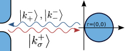
Spin-dependent scattering model. Let us start from a simple model of electron scattering (see Fig. 1). The electron is injected to the system from e.g. a QPC and comes to the potential defect from the left. The defect is taken as an infinite potential step, so that the scattering probability is 1. The incident and backscattered waves are denoted by where stands for the absolute value of the wave vector for the spin state and the superscript sign indicates the electron incoming from the left () or backscattered (). Only the backscattering which returns the carriers to the QPC can alter the conductance, so we consider the scattering wave function along the line between the QPC and the defect
| (1) |
where stand for the scattering amplitudes.
Scattering at other angles does not decrease the conductance and is neglected for a moment. Within the 2DEG, outside the scattering center and the QPC channel the 2D electron Hamiltonian for in-plane field reads
| (2) |
where , , is the electron effective mass, and are the Rashba and Dresselhaus constants. The spin Zeeman effect is introduced via Pauli matrices and the Zeeman energy will be denoted below by .
Note, that we use the symmetric gauge then by choosing the plane of the 2DEG confinement to be located at , we get , and the magnetic field enters the Hamiltonian only via the spin Zeeman term i.e. the orbital effects do not affect the electron transport.
Let us first neglect the Dresselhaus coupling (). Plane wave solution for the eigenvalues of the Schrödinger equation gives
| (3) |
with denoting projections of the spin on the direction of polarization , and eigenvectors
| (4) |
for the incident () and backscattered () directions of the electron motion with . Due to the assumed infinite scattering potential, the wave function in Eq. (1) has to vanish at (see Fig. 1), hence
| (5) |
In the following we use In0.5Ga0.5As material parameters with , Landé factor , and the Fermi energy meV. For the bulk Rashba silva constant Å2, the 2D value is , where is the electric field in the growth-direction. The Rashba constant can be controlled by the external voltages Nitta1997 and for In0.5Ga0.5As SO coupling constants of the order of 5 to 10 meV nm Nitta1997 were recorded.
In Fig. 2(a) we present the scattering amplitudes obtained from Eq. (5) as a function of the direction of the magnetic field , with T for scattering along the direction, . Note that for the magnetic field oriented in the direction , i.e. for the diagonal elements of the scattering amplitudes are zero. This is a special case for which the spinor in Eq. (4) can be written in form where . For a weak magnetic field , we get , and the orthogonality relation , gives zero for the backscattering to states with the same spin projection on the polarization vector (), [see Fig. 2(a)]. On the other hand for high magnetic field , we get , and the spin projection on the polarization vector is conserved .

In Fig. 2(b) we show the evolution of the scattering amplitudes for the orientation of magnetic field fixed at , as a function of the Rashba constant . Then, in Eq. (2) and . The scattering amplitudes cross near meVnm [Fig. 2(b)]. In this point the Zeeman energy is equal to the SO coupling energy . For the off-diagonal terms are: , for which the scattering amplitudes (5) for eigenvectors (4) simplify to for any and for any in-plane orientation of B vector. The case is presented in Fig. 2(a) where the black dashed lines show the scattering amplitudes for T, which shows that almost complete spin mixing is present for any angle.
Let us now include the Dresselhaus SO coupling. The 2D Dresselhaus constant is given by , where is the bulk constant and is the width of the 2DEG confinement in the growth direction. We consider values from 0 to Bernevig2006 ; Koralek2009 . The cubic Dresselhaus interaction is neglected as a small effect Koralek2009 . In the absence of the field, for the electron incident along the direction i.e. , the polarization direction is with the energy eigenvalues . As a result the Dresselhaus interaction sets the direction of the electron spin polarization to and increases the effective SO coupling constant to
The above conclusions can also be reached by a direct inspection of the off-diagonal part of Hamiltonian (2) for the electron transport along the direction (, ). The effective magnetic field in Eq. (2) is . Both components of the effective magnetic field vanish for
| (6) |
and
| (7) |
For illustration we calculated the electron density at the source position – including the incident and backscattered waves using Eqs. (1,5) as . The backscattering probability is roughly proportional to the electron density at the QPC Kolasinski2014Slit . The electron density – is depicted in Fig. 3(b-d) for meVnm, ; and Fig. 3(c-d) meVnm, meVnm. These values produce the same effective coupling constant meVnm.

The results of Fig. 3(b-d) contain a distinct circular pattern in the plane. The position of the center is given by Eqs. (6,7). The angular coordinate of the center allows one to determine the ratio of the Rashba and Dresselhaus constants and the SO coupling constant can be read-out from the position of the center of the pattern on the scale, provided that the Fermi wave vector is known. In presence of SO coupling and / or the Zeeman effect is spin dependent Winkler . However, for the the off-diagonal terms of the Hamiltonian (2) vanish and the Fermi wavevector is directly related to the Fermi energy , which for the adopted parameters gives /nm. For meV nm one obtains meV, which coincides with for T (see Fig. 3(b-d)).
In Fig. 3(c) one notices a reduction of the period with respect to 3(b) with the source-impurity distance increased to 2000 nm from 1500 nm. The period of the oscillations is T in (c), and T in (b). The ratio , is exactly an inverse of the source-impurity distance ratio.
Coherent quantum transport calculations. With the intuitions gained by the simple analytical model we can pass to the calculations of the coherent transport using a standard numerical method Kolasinski2016Lande , based on the quantum transmitting boundary solution of the quantum scattering equation at the Fermi level implemented in the finite difference approach, which produces the electron transfer probability used in the Landauer formula for conductance summed over the subbands of the channels far from the scattering area. Zero temperature is assumed. For the numerical calculations we consider a channel extended along the direction, hence in Eq. (2) remains a quantum number characterizing the asymptotic states of the channel. Within the computational box the wave vector is replaced by an operator .
We consider a QPC/defect system of Fig. 1. The results presented in Fig. 3(a) indicate a reduction of the conductance below the maximal value for subbands passing across the QPC. The central position of the pattern nearly coincides with the one of Fig. 3(c). The local extremum of conductance in the center of the pattern indicates the value and orientation of the external magnetic field which lifts the SO interaction effects. The angular position of Fig. 3(c) is exactly reproduced, and the amplitude of the field is T instead of T. The deviation in the location of the central point in the axis in Fig. 3(a) results from the confinement in the QPC channel which is not included in our free particle model (see below).
The effects described so far dealt with interference of the electron waves between the source (QPC) and the defect. In fact, the role of the source can be played by any scattering center, and the extraction of the SO coupling constant requires a presence of two or more scatterers to allow for formation of standing waves described in the previous section. For the rest of the paper we consider a channel of homogenous width , which carries transport modes at the Fermi level. In Fig. 4(d) we presented the conductance results for a clean channel of width nm and the computational box of length m. A smooth potential barrier is introduced across the channel with height 10 meV and width 200nm. Depending on the orientation of the magnetic field the number of transport modes varies between and . The simulation was performed for meVnm and meVnm as in Fig. 3(b,c). The conductance plot possesses an extremum precisely at the angle of . The magnetic field of the extremum is slightly shifted to lower values than 7.2 T – which is a result of the reduction of within the potential barrier. The lack of conductance oscillations that were observed above in Fig. 3 results from a small barrier length (=200nm).
The oscillations reappear when one replaces the barrier by a random disorder due to the random nonmagnetic and spin-diagonal potential fluctuations. The fluctuations simulate inhomogeneity of the doping of the potential barrier which provides the charge to the 2DEG. In 2DEG in III-V’s due to the spatial separation of the impurities of the 2DEG, the defects do not introduce any significant contribution to the spin-orbit interaction (see Ref. Sellier and the Supplement Supplement ). Figure 4(c) displays the conductance for the channel of the same width and length. The potential – displayed in Fig. 4(a) is locally varied within the range of (-,). The perturbation induces a multitude of scattering evens – the local density of states at the Fermi level for is displayed in Fig. 4(b). In spite of the complexity of the density of states the angular shift is still . The shift of the extremum along the scale with respect to T is detectable – but small and of an opposite sign than in Fig. 4(d). This shift is related to the fact that for a finite width channel is an operator that mixes the subbands. The wave vector is a well-defined quantum number for electrons moving in an unconfined space. The small – but detectable – effects of a finite disappear completely for a wider channel – which is illustrated in Fig. 4(e) for m. Here, the number of conducting bands varies between 80 and 81. The local extremum of conductance appears exactly at the positions indicated in the previous section. Note, that although the number of subbands change by 1 in Fig. 4(c,e), the variation of conductance is as large as in Fig. 4(c) and in Fig. 4(e). The conductance variation in Fig. 3(a) was very small – since the defect was far away from the QPC, for the disordered channel it is no longer the case. For completeness in Fig. 4(f) we presented calculations for a twice smaller SO coupling constants meVnm, meVnm, and meVnm. The position of the maximal along the scale is consistently reduced from 7.2 T to 3.6 T, and the orientation of the magnetic field vector corresponding to the extremum is unchanged.

Summary. We have shown that the in-plane magnetic field can lift the off-diagonal terms of the transport Hamiltonian for the two-dimensional electron gas that result from the Zeeman effect and the SO interaction. The effect appears only for a value and orientation of the external magnetic field which excludes the spin mixing effects that accompany the backscattering in presence of the SO coupling. In consequence the conductance maps for a system containing two or more scatterers – intentionally introduced – or inherently present in a disordered sample exhibit a pronounced extremum as a function of the magnetic field modulus and orientation . An experimental value of – for which the Zeeman energy is equal to the SO coupling energy – should allow one to extract the effective SO coupling constant including both the Rashba and Dresselhaus terms, and the orientation field indicates the relative contributions of both. The results indicate the ratio of the Dresselhaus and Rashba constants is exactly resolved by the procedure, and the amplitude of the magnetic field – hence the effective SO constant varies only within a 10% from the exact value depending on the channel width and disorder profile.
Acknowledgments This work was supported by National Science Centre (NCN) grant DEC-2015/17/N/ST3/02266, and by PL-Grid Infrastructure. The first author is supported by the Smoluchowski scholarship from the KNOW funding and by the NCN Etiuda stipend DEC-2015/16/T/ST3/00310.
References
- (1) A. Manchon, H. C. Koo, J. Nitta, S. M. Frolov, and D. R. A., Nat. Mater. 14, 871 (2015)
- (2) Y. Ohno, R. Terauchi, T. Adachi, F. Matsukura, and H. Ohno, Phys. Rev. Lett. 83, 4196 (1999)
- (3) M. I. D’yakonov and V. I. Perel, JETP Lett. 13, 467 (1971)
- (4) J. Kainz, U. Rössler, and R. Winkler, Phys. Rev. B 70, 195322 (2004)
- (5) J. E. Hirsch, Phys. Rev. Lett. 83, 1834 (1999)
- (6) J. Sinova, D. Culcer, Q. Niu, N. A. Sinitsyn, T. Jungwirth, and A. H. MacDonald, Phys. Rev. Lett. 92, 126603 (2004)
- (7) Y. K. Kato, R. C. Myers, A. C. Gossard, and D. Awschalom, Science 1910, 306 (2004)
- (8) M. Koenig, S. Wiedmann, C. Bruene, A. Roth, H. Buhmann, L. W. Molenkamp, X.-L. Qi, and Z. S.-C., Science 318, 766 (2007)
- (9) B. A. Bernevig, J. Orenstein, and S.-C. Zhang, Phys. Rev. Lett. 97, 236601 (2006)
- (10) J. D. Koralek, C. P. Weber, J. Orenstein, B. A. Bernevig, S.-C. Zhang, S. Mack, and D. D. Awschalom, Nature 458, 610 (2009)
- (11) M. P. Walser, C. Reichl, W. Wegscheider, and G. Salis, Nature Phys. 8, 757 (2012)
- (12) V. Mourik, K. Zuo, S. M. Frolov, S. R. Plissard, E. P. A. M. Bakkers, and L. P. Kouwenhoven, Science 336, 1003 (2012)
- (13) P. Debray, S. M. S. Rahman, J. Wan, R. S. Newrock, M. Cahay, A. T. Ngo, S. E. Ulloa, S. T. Herbert, M. Muhammad, and J. M., Nature Nanotech. 4, 759 (2009)
- (14) S. Datta and B. Das, Appl. Phys. Lett. 56, 665 (1990)
- (15) J. Schliemann, J. C. Egues, and D. Loss, Phys. Rev. Lett. 90, 146801 (2003)
- (16) I. Žutić, J. Fabian, and S. Das Sarma, Rev. Mod. Phys. 76, 323 (2004)
- (17) P. Chuang, S.-C. Ho, L. W. Smith, F. Sfigakis, M. Pepper, C.-H. Chen, J.-C. Fan, J. P. Griffiths, I. Farrer, H. E. Beere, G. A. C. Jones, D. A. Ritchie, and T.-M. Chen, Nat Nano 10, 35 (2015)
- (18) S. Bednarek and B. Szafran, Phys. Rev. Lett. 101, 216805 (2008)
- (19) L. Meier, G. Salis, I. Shorubalko, E. Gini, S. Schoen, and K. Ensslin, Nature Phys. 3 (2007)
- (20) Y. Bychkov and E. Rashba, J. Phys. C 17, 6039 (1984)
- (21) R. Winkler, Spin-orbit Coupling Effects in Two-Dimensional Electron and Hole Systems (Springer-Verlag Berlin Heidelberg, 2003)
- (22) J. Nitta, T. Akazaki, H. Takayanagi, and T. Enoki, Phys. Rev. Lett. 78, 1335 (1997)
- (23) G. Engels, J. Lange, T. Schäpers, and H. Lüth, Phys. Rev. B 55, R1958 (1997)
- (24) I. Lo, J. K. Tsai, W. J. Yao, P. C. Ho, L. W. Tu, T. C. Chang, S. Elhamri, W. C. Mitchel, K. Y. Hsieh, J. H. Huang, H. L. Huang, , and W.-C. Tsai, Phys. Rev. B 65, R161306 (2002)
- (25) J. H. Kwon, H. C. Koo, J. Chang, S.-H. Han, and J. Eom, Appl. Phys. Lett. 90, 112505 (2007)
- (26) D. Grundler, Phys. Rev. Lett. 84, 6074 (2000)
- (27) K.-H. Kim, H.-j. Kim, H. C. Koo, J. Chang, and S.-H. Han, Appl. Phys. Lett. 97, 012504 (2010)
- (28) B. Das, D. C. Miller, S. Datta, R. Reifenberger, W. P. Hong, P. K. Bhattacharya, J. Singh, and M. Jaffe, Phys. Rev. B 39, 1411 (1989)
- (29) Y. Ho Park, H.-j. Kim, J. Chang, S. Hee Han, J. Eom, H.-J. Choi, and H. Cheol Koo, Appl. Phys. Lett. 103, 252407 (2013)
- (30) T. Koga, J. Nitta, T. Akazaki, and H. Takayanagi, Phys. Rev. Lett. 89, 046801 (2002)
- (31) S. D. Ganichev, V. V. Bel’kov, L. E. Golub, E. L. Ivchenko, P. Schneider, S. Giglberger, J. Eroms, J. De Boeck, G. Borghs, W. Wegscheider, D. Weiss, and W. Prettl, Phys. Rev. Lett. 92, 256601 (2004)
- (32) L. Meier, G. Salis, I. Shorubalko, E. Gini, S. Schon, and K. Ensslin, Nature Phys. 3, 650 (2007)
- (33) G. Wang, B. Liu, A. Balocchi, P. Renucci, C. Zhu, T. Amand, C. Fontaine, and X. Marie, Nat. Comm. 4, 2372 (2013)
- (34) S. Meckler, M. Gyamfi, O. Pietzsch, and R. Wiesendanger, Rev. Sci. Instrum. 80, 023708 (2009)
- (35) E. A. de Andrada e Silva, G. La Rocca, and F. Bassani, Phys. Rev. B 55, 16293 (1997)
- (36) K. Kolasiński, B. Szafran, and M. P. Nowak, Phys. Rev. B 90, 165303 (2014)
- (37) J. H. Davies, I. A. Larkin, and E. V. Sukhorukov, J. Appl. Phys 77, 4504 (1995), we apply the formula for the finite rectangle gates, given by equation , where , with meV, nm, nm, (and nm for bottom gate) and (and nm for top gate) and nm. Width of the opening of the QPC is 125nm.
- (38) K. Kolasiński, A. Mreńca-Kolasińska, and B. Szafran, Phys. Rev. B 93, 035304 (2016)
- (39) P. Liu, F. Martins, B. Hackens, L. Desplanque, W. X, M. G. Pala, S. Huant, V. Bayot, and H. Sellier, Phys. Rev. B 91, 075313 (2015)
- (40) K. Kolasiński, H. Sellier, and B. Szafran, Supplemental material