Thermoelectric generation based on spin Seebeck effects
Abstract
The spin Seebeck effect (SSE) refers to the generation of a spin current as a result of a temperature gradient in magnetic materials including insulators. The SSE is applicable to thermoelectric generation because the thermally generated spin current can be converted into a charge current via spin-orbit interaction in conductive materials adjacent to the magnets. The insulator-based SSE device exhibits unconventional characteristics potentially useful for thermoelectric applications, such as simple structure, device-design flexibility, and convenient scaling capability. In this article, we review recent studies on the SSE from the viewpoint of thermoelectric applications. Firstly, we introduce the thermoelectric generation process and measurement configuration of the SSE, followed by showing fundamental characteristics of the SSE device. Secondly, a theory of the thermoelectric conversion efficiency of the SSE device is presented, which clarifies the difference between the SSE and conventional thermoelectric effects and the efficiency limit of the SSE device. Finally, we show preliminary demonstrations of the SSE in various device structures for future thermoelectric applications and discuss prospects of the SSE-based thermoelectric technologies.
KEYWORDS — spintronics; spin current; spin Seebeck effect; inverse spin Hall effect; anomalous Nernst effect; thermoelectric generation; magnetic material; thin film
I INTRODUCTION
Heat is an omnipresent and abundant source of energy, and thus the efficient utilization of thermal energy, such as waste heat recovery and solar heat power generation, is indispensable for the realization of future sustainable society. Thermoelectric generation is one of the promising technologies for making effective use of heat since it enables direct conversion from thermal energy to electrical power DiSalvo1999Science ; Bell2008Science ; Sundarraj2014RSCAdv . As thermoelectric devices consist of solid-state materials and have no moving parts, they are silent, reliable, and scalable. Most of the prevalent thermoelectric generation technologies are based on the Seebeck effect, discovered by T. J. Seebeck in 1821 Rowe ; Goldsmid . Although a variety of thermoelectric effects were found to appear in electric conductors subjected to temperature gradients after the discovery of the Seebeck effect spincaloritronics-Heremans , the earliest thermoelectric phenomenon is still the key player in the thermoelectric technology because of its relatively-high output power and versatility.
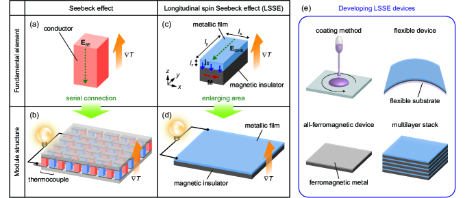
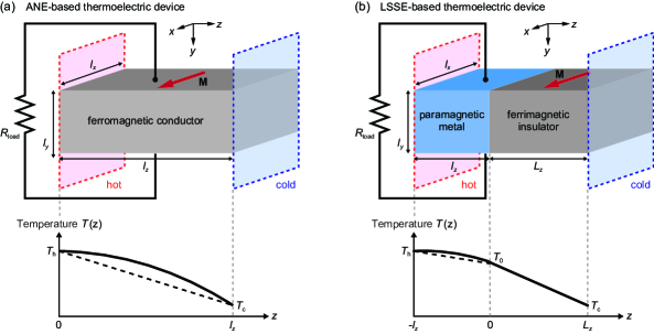
The Seebeck effect refers to the generation of an electric field as a result of a temperature gradient in a conductor, where the direction of is parallel to that of [Fig. 1(a)]. The thermopower induced by the Seebeck effect is represented by the Seebeck coefficient: , which is equal to the ratio of the generated electric voltage to the applied temperature difference owing to the collinear orientation of and . A thermoelectric module based on the Seebeck effect usually consists of a number of -structured thermocouples, i.e., junctions of two materials with different Seebeck coefficients; the thermocouples are serially connected to enhance the thermoelectric output [Fig. 1(b)]. The output voltage of the thermoelectric module can be enhanced in proportion to the number of the thermocouple elements, although such cascaded structure requires costly fabrication processes.
The efficiency of the thermoelectric generation based on the Seebeck effect is characterized by the dimensionless figure of merit , defined as
| (1) |
where , , and are the thermal conductivity, electrical resistivity, and absolute temperature of thermoelectric materials DiSalvo1999Science . The factor is known as a thermoelectric power factor. The efficiency of the Seebeck device for electricity generation is defined as (energy provided to a load)/(heat energy absorbed at the hot end of the device), which is a function of internal and load resistances. The optimized efficiency of the Seebeck device is then given as a function of the figure of merit as follows:
| (2) |
where is the temperature difference between the hot and cold ends of the device, is the temperature at the hot (cold) end, and is the average temperature between the hot and cold ends Rowe ; Goldsmid . Importantly, monotonically increases with increasing ; goes to the Carnot efficiency in the limit of . Therefore, many efforts in thermoelectric research are dedicated to improve the figure of merit of thermoelectric materials.
Equations (1) and (2) mean that materials having a large Seebeck coefficient, low thermal conductivity, and low electrical resistivity are necessary for improving the thermoelectric conversion efficiency. Importantly, low and values make it possible to suppress the energy loss due to heat conduction and Joule dissipation, respectively. However, in isotropic metals, the Wiedemann-Franz law ( with the electronic Lorenz number ) limits this improvement when is dominated by the electronic thermal conductivity . A conventional way to overcome this limitation is to use thermoelectric semiconductors, where the thermal conductance is usually dominated by phonons while the electrical conductance is determined by charge carriers, and thus and are separated according to the kind of the carriers DiSalvo1999Science . Recently, to improve the figure of merit of thermoelectric materials by reducing phonon thermal conductivity without affecting electrical conductivity, not only exploration of new materials SnSe1 ; SnSe2 but also nanotechnology-based phonon engineering TE-nano1 ; TE-nano2 ; TE-nano3 ; TE-nano4 ; TE-nano5 ; TE-nano6 ; TE-nano7 ; TE-nano8 ; TE-nano9 have been conducted. Furthermore, research on the thermoelectric properties of anisotropic materials has attracted increasing attention recently SnSe1 ; SnSe2 ; Morelli_diacetylene ; Balandin_graphene ; Cohn2012PRL ; Butler_2D-review ; Fei_phosphorene ; since the Wiedemann-Franz law is violated in anisotropic materials, they are also useful for optimizing heat and charge conductions separately.
Nearly 200 years after the discovery of the Seebeck effect, a novel thermoelectric generation principle was discovered in the field of spintronics spintronics1 ; spintronics2 ; spincaloritronics-Bauer . This novel principle can be said as a spin counterpart of the Seebeck effect: “spin Seebeck effect” (SSE) SSE_Uchida2008Nature . The SSE refers to the generation of a spin current, a flow of spin angular momentum spincurrent1 ; spincurrent2 , as a result of a temperature gradient in a magnetic material. The SSE is applicable to the construction of thermoelectric generators because the spin current generated by the SSE can be converted into a charge current via the spin-orbit interaction, or the inverse spin Hall effect (ISHE) ISHE_Azevedo ; ISHE_Saitoh ; ISHE_Valenzuela ; ISHE_Costache ; ISHE_Kimura ; ISHE_Sinova , in a conductive thin film (mostly, a paramagnetic metal film) adjacent to the magnetic material (see Sec. II for details). Here, the direction of the electric field induced by the ISHE in the conductive film is perpendicular to that of in the magnetic material [Fig. 1(c)], a configuration different from the conventional Seebeck effect. Since the SSE appears not only in ferromagnetic metals SSE_Uchida2008Nature ; SSE_Uchida2010JAP ; SSE_Bosu2011PRB ; SSE_Uchida2011NatMat ; TSSE_Wang2013PRB and semiconductors SSE_Jaworski2010NatMat ; SSE_Jaworski2011PRL but also in magnetic (mostly, ferrimagnetic) insulators SSE_Uchida2010NatMat ; SSE_Uchida2010APL_1 , it enables the conversion of heat energy in insulators into electrical energy in adjacent conductors SSE_Kirihara2012NatMat ; SSE-Uchida2014JPCM , which was impossible if only conventional thermoelectric technologies were used. The thermoelectric technology based on the SSE is still in an early phase of its development, and the efficiency is very small at the present stage. However, as reviewed in this article, the SSE exhibits various unconventional features suitable for thermoelectric applications.
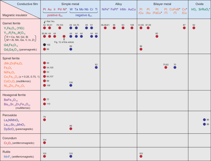
In this review, we focus on the so-called longitudinal SSE (LSSE) SSE_Uchida2010APL_1 ; SSE-Uchida2014JPCM in metallic film/magnetic insulator junction systems, depicted in Fig. 1(c). After the first report on the SSE SSE_Uchida2008Nature , this phenomenon has been measured mainly in two different device structures, i.e., the longitudinal and transverse configurations SSE_Uchida2012JAP , where spin currents parallel and perpendicular to are measured, respectively. The longitudinal configuration has been used in most of the recent SSE studies because the insulator-based LSSE systems are useful for the exclusive detection of spin-current-induced signals and suitable for thermoelectric applications owing to its simple and versatile structure. The first observation of the LSSE was reported in 2010 by using a junction system comprising a paramagnetic metal Pt and a ferrimagnetic insulator Y3Fe5O12 (YIG) SSE_Uchida2010APL_1 . The Pt/YIG junction system is now recognized as a model system for studying SSE physics, since Pt and YIG enable efficient spin-charge conversion and pure detection of spin-current effects, respectively. Since this demonstration, the LSSE has been observed in various combinations of magnetic insulators and conductive films SSE_Uchida2010APL_1 ; SSE_Kirihara2012NatMat ; SSE-Uchida2014JPCM ; SSE_Uchida2012JAP ; SSE_MnZnFO ; SSE-Uchida2011JJAP ; SSE_Weiler2012PRL ; SSE_Uchida2012APEX ; SSE_Qu2013PRL ; SSE_Kikkawa2013PRL ; SSE_Jungfleisch2013APL ; SSE_Meier2013PRB_NFO ; SSE_Ramos2013APL_Fe3O4 ; SSE_Uchida2013PRB ; SSE_Miao2013PRL_PyYIG ; SSE_Schreier2013PRB ; SSE_Kikkawa2013PRB ; SSE_Schreier2013APL ; SSE_Rezende2014PRB ; SSE_Azevedo2014APL_PyYIG ; SSE_BiYIG_Siegel ; SSE_Mendes2014PRB_IrMn ; SSE_Qu2014PRB ; SSE Kehlberger2014JAP ; SSE_time_resolved1 ; SSE_time_resolved2 ; SSE_time_resolved3 ; SSE_Saiga2014APEX ; SSE_Wu2014APL_Fe3O4 ; SSE_Lustikova2014JAP ; SSE_Aqeel2014JAP ; SSE_Wang2014APL ; SSE_Uchida2014PRX ; SSE_Vlietstra2014PRB ; SSE_Xu2014APL ; SSE_BaFe12O19 ; SSE_La2NiMnO6 ; SSE_sign ; SSE_BiYIG_Kikuchi ; SSE_Qiu2015JPD ; SSE_Wu2015JAP_Fe3O4 ; SSE_Sola2015JAP ; SSE_Nd-YIG ; SSE_Niizeki2015AIPAdv_CFO ; SSE_Wu2015PRL ; SSE_Tian2015APL ; SSE_ML_Lee ; SSE_LSMO_La2NiMnO6 ; SSE_Uchida2015PRB_PMA ; SSE_Qu2015PRB_Cr ; SSE_Qiu2015APEX ; SSE_Kikkawa2015PRB ; SSE_Jin2015PRB ; SSE_Kehlberger2015PRL ; SSE_TSeki2015APL ; SSE_Wang2015Nanoscale ; SSE_Kirihara2015IEEE ; SSE_GdIG2016NatCommun ; SSE_ML_Ramos ; SSE_Ritzmann2015 ; SSE_Guo2015 ; SSE_CCO ; SSE_Cr2O3 ; SSE_MnF2 ; SSE_Kirihara2015 ; SSE_Guo2016CFO ; SSE_Zou2016PRB ; SSE_Miao2016AIPAdv ; SSE_Takagi2016BSZFO , as shown in Fig. 2. In contrast, in the transverse configuration, the SSE measurements may be disturbed by thermal conductivity mismatch Huang2011PRL ; Bosu2012JAP between a film and a substrate that induces parasitic LSSE Meier2015NatCommun or anomalous Nernst effect (ANE) spincaloritronics-Heremans ; ANE_Lee2004PRL ; ANE_Miyasato2007PRL ; ANE_Pu2008PRL ; ANE_Mizuguchi2012APEX ; ANE_Sakuraba2013APEX ; ANE_Ramos2014PRB ; ANE_Sakuraba2016 ; ANE_Uchida2015 , requiring careful thermal design of the sample and measurement systems. In the transverse SSE measurements using conductive ferromagnets, a planar Nernst effect (PNE) spincaloritronics-Heremans ; Avery2012PRL ; Schmid2013PRL ; Meier2013PRB ; Soldatov2014PRB may also arise. In the past several years, various thermoelectric measurements have been performed in the transverse configuration Huang2011PRL ; Bosu2012JAP ; Meier2015NatCommun ; Avery2012PRL ; Schmid2013PRL ; Meier2013PRB ; Soldatov2014PRB , and the quantitative separation of the transverse SSE from the parasitic ANE and PNE has been reported in a ferromagnetic metal TSSE_Wang2013PRB . In addition to the longitudinal and transverse configurations, a non-local geometry has also been used recently to investigate the length scale of the SSE Cornelissen2015NatPhys ; Goennenwein2015APL ; Giles2015PRB ; Cornelissen2016PRB .
The LSSE in insulators allows a new approach to improve the thermoelectric figure of merit. In the insulator-based LSSE device, the heat and charge currents flow in different parts of the device: is the thermal conductivity of the magnetic insulator and is the electrical resistivity of the adjacent metal, such that and in the LSSE device are segregated according to the part of the device elements SSE-Uchida2014JPCM . Therefore, the denominator of the figure of merit, , of the LSSE device is free from the Wiedemann-Franz law, and allowed to be optimized if one selects the combination of a magnetic insulator with low thermal conductivity and a metallic film with low electrical resistivity. This is one of the unique characteristics of the LSSE device, although, in addition to the factor, the LSSE thermopower itself must be improved. Importantly, in fact, the relation between the figure of merit and the thermoelectric conversion efficiency of the LSSE device should be different from that of the conventional Seebeck device due to the different device configurations and driving principles SSE_Cahaya2014APL ; SSE_Liao2015Nanoscale ; SSE_Cahaya2015IEEE . One of the purposes of this review article is to formulate the thermoelectric figure of merit and conversion efficiency of the LSSE device, and to clarify the upper limit of the efficiency.
The advantages of the LSSE device include not only the device-design flexibility, discussed above, but also the following characteristics. The LSSE device has convenient scaling capability, where the thermoelectric output increases simply by extending the device area because the total amount of the thermally generated spin currents increases as the device becomes larger SSE_Kirihara2012NatMat . Here, the electric field induced by the ISHE at each point of the LSSE device is integrated into the output LSSE voltage: , where is the magnitude of and is the length of the metallic layer along the direction [Fig. 1(c)]. Since the internal resistance of the metallic layer of the LSSE device is with and respectively being the length along the direction and thickness of the metallic film, the maximum extractable electrical power is proportional to the area of the LSSE device: [see Sec. III.3]. Such a straightforward scaling law makes it possible to enhance the thermoelectric output simply by enlarging the device area [Fig. 1(d)]. To exploit the above characteristics of the LSSE device, versatile and low-cost fabrication methods have been developed, such as coating SSE_Kirihara2012NatMat and plating SSE_Kirihara2015 technologies [Fig. 1(e)]. These methods enable the implementation of simple-structure, large-area, and even flexible LSSE devices onto various heat sources, as shown in Secs. V.1 and V.2.
The thermoelectric generation based on the LSSE involves the following three factors:
-
(1)
heat-current/spin-current conversion efficiency in magnetic materials,
-
(2)
spin-angular-momentum transfer efficiency across metal/insulator interfaces, characterized by the spin mixing conductance spin-mixing ; Jia_spin-mixing_2011EPL ; spin mixing concept ; spin-mixing_Ohnuma ,
-
(3)
spin-current/charge-current conversion efficiency in metallic films, characterized by the spin Hall angle ISHE_Sinova ; Jiao2013PRL .
A direct approach to enhance the performance of the spin-current-driven thermoelectric generation is to improve the LSSE itself [the factor (1)], which realizes efficient thermal spin-current generation [see Sec. V.4]. In addition to this approach, the improvement of the spin mixing conductance [the factor (2)] and the spin Hall angle [the factor (3)] are also essential. For example, to realize the efficient spin-angular-momentum transfer across the metal/insulator interface, the improvement of crystal quality and interface condition of the LSSE device by annealing has been conducted SSE_Saiga2014APEX ; Benjamin_spin-pump_2013APL ; Qiu_spin-pump_2013APL . The spin mixing conductance can also be enhanced by inserting an ultra-thin ferromagnetic interlayer between a paramagnetic metal and a ferrimagnetic insulator owing to the increase of magnetic moment density at the interface SSE_BiYIG_Kikuchi ; Jia_spin-mixing_2011EPL . To realize the efficient spin-charge conversion, the ISHE has been measured in various metals SSE-Uchida2014JPCM ; Morota_2011PRB ; Wang2014PRL ; Singh2015APL , alloys SSE_Miao2013PRL_PyYIG ; SSE_Kikkawa2013PRB ; SSE_Azevedo2014APL_PyYIG ; SSE_Mendes2014PRB_IrMn ; SSE_Wu2014APL_Fe3O4 ; SSE_TSeki2015APL ; SSE_Zou2016PRB ; Niimi2011PRL ; Niimi2012PRL ; Laczkowski2014APL , semiconductors Ando2011NatMat ; Chen2013NatCommun ; Sanchez2013PRB ; Lee2014APL , oxides SSE_LSMO_La2NiMnO6 ; SSE_Qiu2015APEX ; Qiu2012APL ; Fujiwara2013NatCommun , and organic materials Ando2013NatMat ; Qiu2015AIPAdv . The spin mixing conductance and spin Hall angle can be estimated by means of various techniques, such as micro-wave-induced spin pumping ISHE_Azevedo ; ISHE_Saitoh ; Wang2014PRL ; Singh2015APL ; SSE_Azevedo2014APL_PyYIG ; SSE_Mendes2014PRB_IrMn ; Laczkowski2014APL ; Ando2011NatMat ; Chen2013NatCommun ; Sanchez2013PRB ; Lee2014APL ; Qiu2012APL ; Ando2013NatMat ; Qiu2015AIPAdv ; Silsbee1979PRB ; Tserkovnyak2002PRL ; Mizukami2002PRB ; Kajiwara2010Nature , spin Hall magnetoresistance Chen2013PRB ; Nakayama2013PRL ; Hahn2013PRB ; Vliestra2013PRB ; Althammer2013PRB , and non-local methods ISHE_Valenzuela ; ISHE_Kimura ; Morota_2011PRB ; Niimi2011PRL ; Niimi2012PRL ; Laczkowski2014APL ; Fujiwara2013NatCommun ; Jedema2001Nature ; Jedema2002Nature ; Niimi2015RepProgPhys , where these phenomena can be measured by applying microwaves or charge currents to similar paramagnet/ferromagnet junction systems instead of temperature gradients. Therefore, not only the LSSE experiments but also these techniques are necessary for optimizing the LSSE devices. Although the conventional LSSE experiments have mainly been performed using paramagnetic metal/ferrimagnetic insulator junction systems, all-ferromagnetic devices SSE_Miao2013PRL_PyYIG ; SSE_Kikkawa2013PRB ; SSE_Azevedo2014APL_PyYIG ; SSE_TSeki2015APL , i.e., ferromagnetic metal/ferrimagnetic (or ferromagnetic) insulator junction systems, and alternately-stacked metal/insulator multilayer films SSE_ML_Ramos have recently been recognized as useful tools for improving the thermoelectric performance of the LSSE devices, as shown in Secs. V.3 and V.4.
In this article, we review recent studies on the LSSE from the viewpoint of thermoelectric applications. This article is organized as follows. We start with an explanation of the thermoelectric generation process and measurement configuration of the LSSE in Sec. II, followed by experimental demonstrations of the basic characteristics of the LSSE devices in Sec. III. In Sec. IV, we formulate the thermoelectric figure of merit and conversion efficiency of the LSSE devices and compare the results with those for conventional thermoelectric devices. In Sec. V, we show preliminary demonstrations for future thermoelectric applications of the LSSE devices, where we focus on the device structures depicted in Fig. 1(e). The last Sec. VI is devoted to the conclusions and prospects.
II Thermoelectric generation process and measurement configuration
Figure 3(a) shows a schematic illustration of the standard configuration used for the LSSE measurements. The basic structure of the LSSE device consists of a metallic film formed on a magnetic insulator. Here, the magnetic insulator is a slab without a substrate or a film formed on a substrate, while the metallic layer must be a thin film as explained later. In the metal/insulator junction in the longitudinal configuration, the temperature gradient, , is applied perpendicular to the metal/insulator interface (along the direction) and the spatial direction of the spin current induced by the LSSE is parallel to the direction SSE_Uchida2010APL_1 . The LSSE is usually measured with applying an external magnetic field to align the magnetization of the magnetic insulator along the direction [Fig. 3(a)]. However, the external magnetic field is not indispensable for the LSSE-based thermoelectric generation if the device comprises a hard-magnetic material SSE_BaFe12O19 ; SSE_Niizeki2015AIPAdv_CFO . Under this condition, a DC electric voltage difference between the ends of the metallic film of the LSSE device is measured.
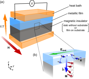
To apply the temperature gradient in the direction perpendicular to the metal/insulator interface, the LSSE device is usually sandwiched between two heat baths which are stabilized at different temperatures [Fig. 3(a)] SSE_Uchida2010APL_1 ; SSE-Uchida2014JPCM . By heating or cooling the heat baths, one can apply a reversible temperature gradient to the LSSE device since its top and bottom surfaces are directly connected to the heat bath SSE_Uchida2012JAP . Owing to this high temperature controllability, the setup depicted in Fig. 3(a) is mostly used in the LSSE measurements; all the experiments shown in this article were performed in this setup. In contrast, the temperature gradient can be applied to the LSSE device also by using Joule heating in an on-chip heater SSE_Wu2014APL_Fe3O4 ; SSE_Vlietstra2014PRB ; SSE_Xu2014APL ; SSE_Wu2015JAP_Fe3O4 , laser heating SSE-Uchida2011JJAP ; SSE_Weiler2012PRL ; SSE_Schreier2013PRB ; SSE_time_resolved1 ; SSE_time_resolved2 , and microwave heating SSE_Jungfleisch2013APL ; SSE_time_resolved3 . Although these methods enable the measurements of the LSSE without using the specialized temperature-gradient generators, it is difficult to determine the temperature distributions; the methods are sometimes combined with numerical simulations SSE_Wu2015JAP_Fe3O4 ; SSE_Weiler2012PRL ; SSE_Schreier2013PRB ; SSE_time_resolved2 ; SSE_time_resolved3 .
The thermoelectric generation mechanism of the LSSE device is summarized as follows. The driving force of the LSSE is nonequilibrium dynamics of magnons, collective excitations of localized magnetic moments, in the magnetic insulator driven by the temperature gradient SSE_Xiao2010PRB ; SSE_Adachi2010APL ; SSE_Adachi2011PRB ; SSE_Ohe2011PRB ; SSE_Bender2012PRL ; SSE_Ohnuma2013PRB ; SSE_Adachi2013review ; SSE_Hoffman2013PRB ; SSE_Chotorlishvili2013PRB ; SSE_Ren2013PRB ; SSE_Bender2015PRB ; SSE_Lyapilin2015PRB ; SSE_Etesami2015APL ; SSE_Brataas2015PRB ; SSE_Chotorlishvili2015JMMM ; SSE_Rezende2016PRB ; SSE_Xiao2015 , since the LSSE appears even when a conduction electrons’ contribution is completely frozen out. This nonequilibrium magnon dynamics in the magnetic insulator can interact with conduction-electron spins in the attached metal and transfer the spin angular momentum across at the metal/insulator interface via the interface s-d exchange interaction, which is described in terms of the spin mixing conductance spin-mixing ; Jia_spin-mixing_2011EPL ; spin mixing concept ; spin-mixing_Ohnuma . This spin-angular-momentum transfer induces a conduction-electron spin current in the metallic film. This spin current is converted into the electric field, , by the aforementioned ISHE in the metallic layer if the spin-orbit interaction of the metal is strong [Fig. 3(b)]. When the magnetization of the magnetic insulator is aligned along the direction, is generated in the metallic film along the direction according to the relation spincurrent1
| (3) |
where , , and are the spin Hall angle, unit vector along the electron-spin polarization () in the metallic layer, and spatial direction of the spin current (with the magnitude of spin current density ) induced by the LSSE, respectively. Thus, the thermoelectric voltage can be generated by the combination of the LSSE and ISHE and observed by measuring the voltage between the ends of the metallic layer, where the sign of is determined by that of (Fig. 2) SSE-Uchida2014JPCM . This thermoelectric generation mechanism works below the Curie temperature of the magnetic insulator SSE_Uchida2014PRX . Here, to detect the LSSE voltage, the thickness of the metallic layer has to be comparable to its spin diffusion length ISHE_Sinova ; Jiao2013PRL , typically a few to several hundreds of nanometers, since the spin current injected into the metallic layer and the resultant exist only in the vicinity of the metal/insulator interface due to the spin relaxation. We also note that, when a highly resistive insulator is used, the contribution from thermoelectric phenomena in itinerant magnets, such as the conventional Seebeck and Nernst effects, is eliminated in the LSSE device SSE_Uchida2010APL_1 ; SSE_Kikkawa2013PRB .
III Basic characteristics of spin Seebeck devices
In this section, by using the Pt/YIG model systems, we demonstrate the basic characteristics of the LSSE devices, such as the dependence of the thermoelectric voltage on the temperature, temperature gradient and its direction, magnetic field and its direction, and device geometry.
III.1 Fundamental experiments
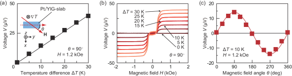
Here, we show the fundamental properties of the LSSE SSE-Uchida2014JPCM ; SSE_Kikkawa2013PRL ; SSE_Kikkawa2013PRB . The Pt/YIG junction system used here consists of a single-crystalline YIG slab and a Pt film sputtered on the well-polished surface of the YIG. The lengths of the Pt film (YIG slab) along the , , and directions are (), (), and (), respectively. To generate along the direction, the temperatures of the heat baths attached to the top and bottom of the Pt/YIG-slab sample were stabilized to and , respectively. The external magnetic field (with the magnitude ) was applied to the Pt/YIG-slab sample in the - plane at an angle to the direction [see the inset to Fig. 4(a)].
Figure 4(a) shows between the ends of the Pt film in the Pt/YIG-slab sample as a function of at . When was applied along the direction (), the magnitude of was found to be proportional to . As shown in Fig. 4(b), the sign of for finite values of is reversed in response to the sign reversal of , indicating that the signal in the Pt film is affected by the magnetization direction of the YIG slab (note that the magnetization of the YIG slab is aligned along the direction when ). To confirm the origin of this signal, we also measured the dependence of in the same Pt/YIG-slab sample at and [Fig. 4(c)]. The signal was observed to vary with in a sinusoidal pattern and vanish when and , a situation consistent with the symmetry of the ISHE induced by the LSSE described in Eq. (3).
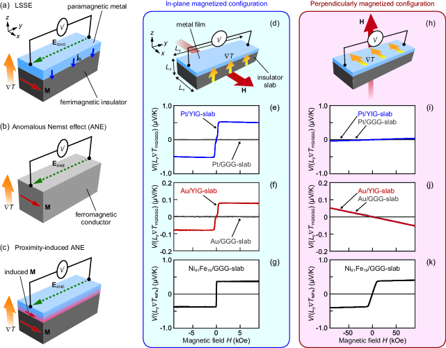
The above experiments indicate that the observed thermoelectric voltage is attributed to the LSSE. However, to exclusively establish the LSSE, the contribution of the LSSE has to be separated from that of the ANE spincaloritronics-Heremans . Since Pt is a paramagnetic metal and YIG is a very good insulator, the ANE does not exist in the Pt/YIG system in the ordinary sense. In this system, however, weak ferromagnetism may be induced in the Pt layer in the vicinity of the Pt/YIG interface due to a static magnetic proximity effect Huang2012PRL ; Geprags_2012APL_XMCD ; Chien_2013PRL_XMCD ; Geprags_2013arXiv_XMCD ; Sun2013PRL ; Miao2014PRL ; proximity-ANE_Guo ; Haertinger2015PRB because Pt is near the Stoner ferromagnetic instability DoS ; Ibach . In fact, when the thickness of Pt is very thin (), weak ferromagnetic signals were observed by means of X-ray magnetic circular dichroism Geprags_2012APL_XMCD ; Chien_2013PRL_XMCD ; Geprags_2013arXiv_XMCD . If the proximity-induced ferromagnetism induces the ANE in the Pt layer, the ISHE voltage induced by the LSSE in the Pt/YIG system may be contaminated by the proximity-induced ANE in the Pt layer. This possibility was pointed out by Huang et al. in 2012 on the basis of magnetoresistance and Hall measurements Huang2012PRL , although the anisotropic magnetoresistance in Pt/YIG systems was subsequently shown to be attributed to the spin Hall magnetoresistance Chen2013PRB ; Nakayama2013PRL ; Hahn2013PRB ; Vliestra2013PRB ; Althammer2013PRB . Here, the electric field induced by the ANE is generated according to the relation SSE-Uchida2014JPCM
| (4) |
where is the anomalous Nernst coefficient. This configuration is similar to that of the LSSE since is generated along the direction when and [compare Figs. 5(a)-5(c)]. After the problem presentation by Huang et al., the pure detection of the LSSE was realized by using Au/YIG systems SSE_Qu2013PRL ; SSE_Kikkawa2013PRL , where Au is free from the magnetic proximity effect because its electronic structure is far from the Stoner instability DoS . To investigate the magnetic proximity effect in Pt/YIG systems, microwave spectroscopy measurements were also carried out Sun2013PRL ; Haertinger2015PRB . Guo et al. theoretically investigated the proximity-induced ANE in Pt and Pd within Berry-phase formalism based on relativistic band-structure calculations proximity-ANE_Guo .
The clear separation of the LSSE from the proximity-induced ANE was reported in SSE_Kikkawa2013PRL ; SSE_Kikkawa2013PRB by comparing transverse thermoelectric voltage in the Pt/YIG system in in-plane magnetized (IM) and perpendicularly magnetized (PM) configurations. In the IM (PM) configuration, is applied parallel (perpendicular) to the Pt/YIG interface and is applied perpendicular (parallel) to the interface, as shown in Fig. 5(d) [5(h)]. The IM configuration is the same as the LSSE setup (Fig. 3), where both the LSSE and ANE can appear if they exist. In the PM configuration, the ANE signal can appear since the temperature gradient, magnetization, and inter-electrode direction are at right angles to one another [Eq. (4)], while the LSSE voltage should disappear due to the symmetry of the ISHE [Eq. (3)], where in the PM configuration. Therefore, the quantitative comparison of the voltage between these configurations enables the estimation of the ANE contamination in the Pt/YIG system.
Figures 5(e) and 5(i) show the dependence of the voltage normalized by the device length along the direction and the temperature gradient in the YIG slab, , in the Pt/YIG-slab sample in the IM and PM configurations, respectively SSE-Uchida2014JPCM ; SSE_Kikkawa2013PRB . The magnitude of in the IM configuration was found to be much greater than that in the PM configuration. Here, the magnitude of the normal Nernst voltage, which is the -linear component of , in the Pt/YIG-slab sample in the PM configuration is comparable to that in the Pt/paramagnetic Gd3Ga5O12 (GGG)-slab sample and in a Pt plate without a substrate SSE_Kikkawa2013PRB , confirming that the in-plane temperature gradient is generated in the Pt/YIG-slab sample in the PM configuration (note that the Pt/GGG-slab sample exhibits only a normal Nernst effect and no LSSE voltage except at very low temperatures SSE_Wu2015JAP_Fe3O4 ). The voltage behavior in the Pt/YIG-slab sample is completely different from that in a ferromagnetic Ni81Fe19 film on a GGG substrate, where only the ANE and small normal Nernst effect appear; in the Ni81Fe19 film, the isotropic ANE voltage was observed in both the IM and PM configurations, when the voltage is normalized by the temperature gradient in the Ni81Fe19 film [Figs. 5(g) and 5(k)] SSE-Uchida2014JPCM ; SSE_Kikkawa2013PRB . The above results clearly show that the transverse thermoelectric voltage in the Pt/YIG system is dominated by the ISHE voltage induced by the LSSE and that the proximity-ANE contamination is negligibly small. In SSE_Kikkawa2013PRB , the contribution of the proximity-induced ANE voltage in the Pt/YIG system was estimated to be less than 0.1 % of the LSSE voltage. As shown in Figs. 5(f) and 5(j), similar results were obtained in Au/YIG systems.
The experimental results shown in Fig. 5 clearly demonstrate that the thermoelectric voltage in the Pt/YIG system is due entirely to the ISHE induced by the LSSE. Although the separation of the LSSE from the ANE is very important from the viewpoint of fundamental physics, even the proximity-induced ANE should be utilized effectively from the viewpoint of thermoelectric applications because the thermoelectric output of the LSSE device might be enhanced by the superposition of the proximity-induced ANE voltage. Recently, to validate the availability of the proximity-induced ANE, we investigated the ANE in alternately-stacked Pt/Fe multilayer films, which were designed to enhance the proximity-induced ANE intentionally; the proximity-ANE contribution in the Pt/Fe multilayer films is expected to be up to two orders of magnitude greater than that in the conventional Pt/YIG system ANE_Uchida2015 . However, even in these multilayer systems, no clear evidence for the existence of the proximity-induced ANE was observed. Therefore, the potential of the magnetic proximity effect as a thermoelectric generation mechanism is still unknown. In contrast, the standard ANE in ferromagnetic materials has already been investigated as a novel thermoelectric conversion technology ANE_Sakuraba2013APEX ; ANE_Sakuraba2016 . Especially, we focus on ferromagnetic metals as conductive layer materials of the LSSE device since they enable the hybrid thermoelectric generation by the LSSE and ANE SSE-Uchida2014JPCM and replacement of noble metals, such as Pt and Au, in the LSSE device, as discussed in Sec. V.3.
III.2 High magnetic field dependence
Recently, several research groups reported the investigation of the high-magnetic-field response of the LSSE in Pt/YIG systems with different YIG thicknesses at various temperatures SSE_Kikkawa2015PRB ; SSE_Jin2015PRB ; SSE_Ritzmann2015 ; SSE_Guo2015 . These studies provide a significant guideline for optimizing the thickness of the magnetic insulator layer of the LSSE device since the high-magnetic-field dependence of the LSSE was found to be associated with the characteristic lengths of the LSSE. In this subsection, with showing our experimental results for the Pt/YIG systems SSE_Kikkawa2015PRB , we review the behavior of the LSSE in a high magnetic field range and its interpretation.
The observation of the SSE in insulators revealed that the magnon excitation plays a key role in this phenomenon. After the pioneering theoretical work by Xiao et al. SSE_Xiao2010PRB , the SSE is mainly described in terms of the effective magnon temperature in a ferrimagnetic insulator and effective electron temperature in an attached paramagnetic metal; when the effective magnon-electron temperature difference is induced by an external temperature gradient, a spin current is generated across the ferrimagnet/paramagnet interface due to the thermal spin pumping. Subsequently, Adachi et al. developed linear-response theories of the magnon- and phonon-mediated SSEs SSE_Adachi2010APL ; SSE_Adachi2011PRB ; SSE_Adachi2013review . Hoffman et al. formulated a Landau-Lifshitz-Gilbert theory of the SSE to investigate the thickness dependence and length scale of the SSE SSE_Hoffman2013PRB . In 2014, Rezende et al. discussed the SSE in terms of a bulk magnon spin current created by a temperature gradient in a ferrimagnetic insulator SSE_Rezende2014PRB . Furthermore, various theoretical models of the magnon-driven SSE were also developed SSE_Ohe2011PRB ; SSE_Bender2012PRL ; SSE_Ohnuma2013PRB ; SSE_Chotorlishvili2013PRB ; SSE_Ren2013PRB ; SSE_Bender2015PRB ; SSE_Lyapilin2015PRB ; SSE_Etesami2015APL ; SSE_Brataas2015PRB ; SSE_Chotorlishvili2015JMMM ; SSE_Rezende2016PRB ; SSE_Xiao2015 . However, microscopic understanding of the relation between the magnon excitation and thermally generated spin current is yet to be fully established, and more detailed studies are necessary. Since the magnon excitation is modulated by a magnetic field due to the Zeeman gap , the ISHE voltage induced by the SSE can also be affected by the magnetic field. Therefore, systematic measurements of the magnetic-field-induced response of the SSE become powerful tools for unraveling the thermo-spin conversion mechanism based on the magnon excitation.
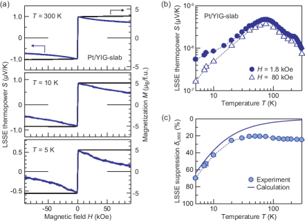
In Fig. 6(a), we show the transverse thermopower in the Pt/YIG-slab sample as a function of for several values of the temperature , measured when was swept between . The clear LSSE voltage was observed in the Pt/YIG-slab sample at all the temperatures and its magnitude at each temperature gradually decreases with increasing after taking the maximum value, while the magnitude of is almost constant after the saturation. This suppression of the LSSE voltage becomes apparent by applying high magnetic fields, while it is very small in the conventional LSSE measurements in a low field range. The suppression of the LSSE voltage was shown to be irrelevant to the normal Nernst effect in the Pt film SSE_Kikkawa2015PRB .
The magnetic-field-induced suppression of the LSSE voltage in the Pt/YIG-slab sample increases with decreasing the temperature. Figure 6(c) shows the dependence of the suppression of the LSSE thermopower in the same Pt/YIG-slab sample, where is defined as with and respectively being the values at the maximum point and at [the dependence of at the positive values is shown in Fig. 6(b)]. The field-induced suppression in the Pt/YIG-slab sample was observed to be almost constant above 30 K and strongly enhanced below 30 K; the value in the Pt/YIG-slab sample reaches 70 % at . The field-induced suppression of the LSSE for cannot be explained by the conventional SSE models, while that for seemingly agrees with numerical calculations based on the thermal spin pumping mechanism [Fig. 6(c)] (see SSE_Kikkawa2015PRB for details). The inconsistency between the observed suppression of the LSSE voltage and the conventional formulation at relatively-high temperatures is attributed to the fact that the small Zeeman energy is defeated by thermal fluctuations when in the conventional models, where , , and are the -factor, Bohr magneton, and Boltzmann constant, respectively (note that the magnon gap energy at corresponds to ); to affect the magnon excitation by magnetic fields, the magnon energy has to be comparable to or less than the Zeeman energy. In contrast, the observed large suppression of the LSSE voltage in the Pt/YIG-slab sample indicates that the magnon excitation relevant to the LSSE is affected by magnetic fields even at around room temperature. This result suggests that low-frequency magnons of which the energy is comparable to the Zeeman energy provide a dominant contribution to the LSSE; the thermo-spin conversion efficiency of the LSSE has magnon-frequency dependence, which is not included in the conventional SSE theories. In SSE_Kikkawa2015PRB and SSE_Rezende2016JMMM , the origin of this spectral non-uniform thermo-spin conversion is discussed in terms of the frequency dependence of a magnon thermalization (energy relaxation) length and a magnon diffusion length, respectively. It is notable that lower frequency magnons exhibit the longer characteristic lengths in general SSE_Xiao2010PRB ; SSE_Rezende2016JMMM ; Sanders-Walton ; SSE_Zhang-Zhang_2012PRL ; SSE_Zhang-Zhang_2012PRB ; Agrawal2013PRL ; Ruckriegel2014PRB ; YIG_kappa_Boona-Heremans ; Cornelissen2015NatPhys ; Goennenwein2015APL ; Giles2015PRB ; Cornelissen2016PRB .
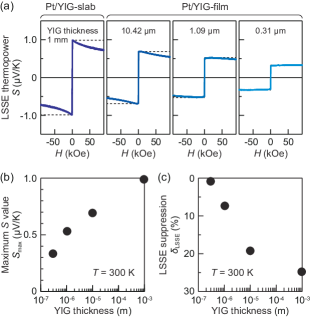
The above results and discussions indicate that, to maximize the thermoelectric output of the LSSE device, the thickness of the magnetic insulator has to be greater than the characteristic lengths of low-frequency magnons providing a strong contribution to the LSSE, since the contribution from the long-range magnons can be limited by boundary conditions in thin magnetic insulators SSE_Kikkawa2015PRB . In fact, several research groups demonstrated that, by using the Pt/YIG-slab and Pt/YIG-film systems, the magnitude of the LSSE thermopower monotonically decreases with decreasing the thickness of YIG [our experimental results are shown in Figs. 7(a) and 7(b)] SSE_Kikkawa2015PRB ; SSE_Kehlberger2015PRL ; SSE_Guo2015 . Significantly, the suppression of the LSSE by high magnetic fields, , also monotonically decreases with decreasing the YIG thickness [Figs. 7(a) and 7(c)]. This behavior indicates that the contribution of low-frequency magnons, which govern the LSSE suppression in the Pt/YIG-slab sample, fades away in the Pt/YIG-film samples when the YIG thickness is less than their characteristic lengths and that only remaining contribution from high-frequency magnons, which have energy much greater than the Zeeman energy and provide a weak contribution to the LSSE, appears in the thin YIG-film samples. As reviewed in this subsection, the measurements of the high-magnetic-field response of the LSSE are useful for characterizing the properties of the LSSE devices associated with magnon excitation.
III.3 Current-voltage-power characteristics and scaling law
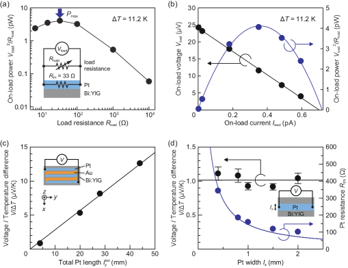
Now we demonstrate the current-voltage-power characteristics of the LSSE device by using a Pt/BiY2Fe5O12 (Bi:YIG) bilayer film SSE-Uchida2014JPCM . To determine the characteristics, we attached a load resistance to the Pt layer and measured the voltage across the load resistance to estimate the output power with changing the value, while most of the LSSE experiments have been performed under the open-circuit condition. In Fig. 8(a), we show generated from the Pt/Bi:YIG-film sample at as a function of . We found that the maximum output power can be extracted when is equal to the internal resistance of the Pt layer: . This behavior is also confirmed by the linear current-voltage relation and parabolic current-power relation for the Pt/Bi:YIG-film sample in Fig. 8(b). The current-voltage-power characteristics and optimizing condition for the load resistance for the LSSE devices are the same as those for any linear generators, such as batteries and conventional thermoelectric modules.
Next, we experimentally verify the scaling law of the LSSE device: the output power is proportional to the device area, introduced in Sec. I. To do this, we investigated the dependence of the LSSE voltage on the size, i.e., length and width, of the metallic layer of the LSSE device as follows SSE_Kirihara2015IEEE .
For measuring the metallic-layer-length dependence of the LSSE, we used the structure called “spin Hall thermopile” SSE_Uchida2012APEX . The spin Hall thermopile consists of an alternating array of two different metallic wires with different spin Hall angles, connected in series in a zigzag configuration. The sample used here is the spin Hall thermopile comprising 10-nm-thick Pt wires and 30-nm-thick Au wires formed on a Bi:YIG film [see the inset to Fig. 8(c)]. In this sample, the LSSE voltage in each wire is integrated into the total voltage between the ends of the Pt-Au thermopile and the total voltage predominantly comes from the Pt wires, because the spin Hall angle and resistivity of Pt are greater than those of Au and the thickness of the Pt wires is less than that of the Au wires (note that the magnitude of the LSSE voltage increases with decreasing the thickness of the metallic layer except for ultrathin regions SSE_Kikkawa2013PRB ; SSE_Qu2014PRB ; SSE_Saiga2014APEX ). Figure 8(c) shows the dependence of the LSSE voltage per unit temperature difference, , on the total length of the Pt wires in the Pt-Au thermopile, where is changed by changing the number of the Pt-Au pairs. As expected above, the magnitude of increases in proportion to .
In addition to the Pt-length dependence, we also investigated the Pt-width dependence. We fabricated Pt films with different widths on fixed-size Bi:YIG films, where the length and thickness of the Pt films are fixed [see the inset to Fig. 8(d)]. In Fig. 8(d), and the Pt-film resistance are plotted as a function of the Pt width . We found that the magnitude of is almost independent of , while is inversely proportional to .
The obtained scaling results, i.e., and , clearly indicate that a larger film area leads to larger thermoelectric output power that can be extracted to an external load. Here, we would like to emphasize again that the scaling law of the LSSE devices is quite different from that of conventional thermoelectric devices based on the Seebeck effect, where the thermoelectric output scales with the number of thermocouples connected in series (see Sec. I and Fig. 1).
IV Theory of efficiency of spin Seebeck thermoelectric devices
In this section, we present a theory of the efficiency of thermoelectric devices based on the LSSE. First, we give a brief review of the efficiency of thermoelectric generators based on the ANE. This is because the ANE has a similarity to the LSSE in that the induced electric field is orthogonal to the applied temperature gradient, and a thermoelectric device possessing this characteristic is called a transverse device Goldsmid . Next, based on the discussion of the ANE generators, we formulate the efficiency of the LSSE devices.
IV.1 Review of efficiency of thermoelectric generators based on anomalous Nernst effects
As pointed out above, it is quite instructive to review the efficiency calculation of the ANE device Harman62 ; Harman62-2 ; Harman63 . We begin with the following transport equations Landau-Elec :
| (5) | |||||
| (6) |
where , , and are an applied electric field, charge current density (with the magnitude ), and heat current density, respectively. is the Peltier coefficient. The (anomalous) Hall coefficient is disregarded as it is irrelevant to the present discussion, and the Leduc-Righi coefficient thermal-Hall1 ; thermal-Hall2 is assumed to be negligibly small. Here we note that the following discussion is applicable not only to the ANE devices but also to normal Nernst devices spincaloritronics-Heremans if the spontaneous magnetization is replaced with an external magnetic field, while this article focuses on the comparison between the LSSE and ANE devices because of their similar characteristics. It should also be added that the thermoelectric conversion efficiency of normal Nernst generators, or Ettingshausen coolers, in semimetals can be much greater than that of the ANE and LSSE devices, although an external magnetic field must be applied Yim72 .
We first calculate the amount of heat evolved per unit time and volumes, which governs the temperature profile of the system in the steady state. This quantity is given by Landau-Elec , where is the energy current density with being the electrochemical potential. Using Eqs. (5) and (6), we obtain
| (7) | |||||
where the first and second terms on the right hand side represent the Joule heating and thermal conduction. The third term, which comes from the temperature dependence of the Seebeck coefficient via the relation , is the Thompson effect and will be neglected hereafter to simplify the argument. Besides, since the last term can be interpreted as a change in the Thompson effect due to the presence of magnetization Landau-Elec , this term is also discarded. Therefore, by considering the conservation law of energy flux, i.e., , we obtain the following equation:
| (8) |
which determines the temperature distribution in thermoelectric devices, known as Domenicali’s equation Domenicali54 .
Let us focus on the ANE device shown in Fig. 9(a). Here, a temperature gradient () is applied along the axis, and an external magnetic field is applied along the axis to align the magnetization, . Under the isothermal condition () as well as the open circuit condition (), the ANE induces an electric field along the axis, and a charge current density is driven in the direction, i.e., . Since the electromotive force is given by
| (9) |
and the total resistance in the circuit is given by with and respectively being the internal and load resistances, the resultant charge current is calculated to be
| (10) |
where we have introduced a dimensionless variable .
Now we discuss the efficiency of the ANE device. The efficiency is defined by
| (11) |
where is the electrical power output and is the thermal power input from the hot reservoir. The latter quantity is calculated as follows Heikes61 ; Mahan98 . First, we assume a uniform charge current distribution along the direction, i.e., . Then, from Domenicali’s equation [Eq. (8)] under the condition and , the temperature distribution is calculated to be
| (12) |
where the distribution of is schematically shown in Fig. 9(a). Next, we evaluate the magnitude of the heat current at the hot reservoir, i.e., , using Eq. (6). Then, the rate of heat removal from the hot reservoir, defined by , is calculated to be
| (13) |
where is the thermal conductance in the direction and is the electrical resistance in the direction.
From Eqs. (11)-(13), the efficiency is expressed as a function of :
| (14) |
where is the Carnot efficiency. Here, the characteristic function,
| (15) |
is defined by the isothermal figure of merit
| (16) |
where is the thermal conductivity at zero electric field. Note the minus sign in the first term of the denominator in Eq. (15), which is peculiar to transverse devices Harman62 . By maximizing with respect to , the optimized efficiency in the limit of is calculated to be
| (17) | |||||
| (18) |
where the functional form is quite different from the conventional Seebeck device because of the fact that the ANE device has a symmetry of transverse devices. Note that, by contrast, the maximum power output is given by the impedance matching condition as is well known Heikes61 .
Two comments are in order. First, according to the argument of Horst63 and Delves64 , the isothermal figure of merit in Eq. (15) is related to the adiabatic figure of merit as
| (19) |
such that , where is the thermal conductivity at zero charge current. Therefore, the maximum allowed efficiency is obtained for (i.e., ), achieving the Carnot efficiency: . Second, the figure of merit in Eq. (16) is determined by the thermal conductivity and the electrical resistivity that are defined in the same material.
IV.2 Efficiency of thermoelectric generators based on spin Seebeck effects
In this subsection, based on the discussion in the previous subsection, we discuss the efficiency of the LSSE device. We consider a device shown in Fig. 9(b), where a bilayer of a paramagnetic metal P and a ferrimagnetic insulator F is sandwiched between hot and cold reservoirs. We assume that the thermal conductivity of P is much greater than that of F , such that the temperature gradient develops inside F and thus the temperature gradient inside P is negligibly small in comparison to F. Looking at Table I given in SPE_Flipse2014PRL , this assumption seems moderately reasonable. Note that we made this assumption in order to keep the mathematical manipulations manageable and to extract a simple analytical expression; otherwise such a simple result would never be obtained and a more involved numerical approach would be required, which is beyond our scope. Also, we assume that there is no discontinuous jump in the temperature distribution at the P/F interface. In this sense, the present approach is complementary to the calculation in SSE_Cahaya2014APL , where only the temperature difference at the P/F interface was considered as a driving force. Instead, we assume that the temperature is a smooth function across the P/F interface, and the temperature at the interface is determined by the heat current conservation. Here, the relationship between the present continuous temperature model and a three temperature model used in SSE_Schreier2013PRB ; SSE_Cahaya2014APL ; SSE_Xiao2010PRB is given in the following way. The present approach is constructed based on the formalism developed in SSE_Zhang-Zhang_2012PRB , and the magnon accumulation [see Eq. (11) of SSE_Zhang-Zhang_2012PRB ] corresponds to the effective magnon-phonon temperature difference. It has been demonstrated that the present single temperature gradient model provides us with an excellent description of the SSE in magnetic multilayers SSE_ML_Ramos .
We start our discussion from the following transport equations for P:
| (20) | |||||
| (21) | |||||
| (22) |
where is the spin voltage gradient and is the electrical conductivity of P. For F, we assume the following transport equations:
| (23) | |||||
| (24) |
where in F is determined by the magnon density gradient , is the magnon conductivity, and () is the magnon Seebeck (Peltier) coefficient. Here, the thermal conductivity of F includes both magnon contribution as well as phonon contribution , and Onsager’s reciprocity SPE_Flipse2014PRL requires .
Let us first calculate the open circuit voltage under a temperature bias between the hot and cold reservoirs. As stated before, because of the condition , the temperature gradient develops inside F as . According to Eq. (23), this temperature gradient drives a spin current inside F, which then injects an amount of
| (25) |
into P, where the coefficient () represents the ratio of the spin current injected into P to the thermal drift magnon current in F. Note that the parameter is proportional to the spin mixing conductance. If we adopt an approach of SSE_Rezende2014PRB and SSE_Zhang-Zhang_2012PRB where the continuity of at the P/F interface is postulated, the constant is given by , where is the magnon diffusion length of F. Inside P, thanks to the ISHE [Eq. (20)], the injected spin current is converted into a charge current when . Then, in the open circuit condition, this current is compensated by an electromotive force
| (26) |
where . Here, the factor in comes from averaging over the thickness of P, where we approximated the hyperbolic variation of by a linear curve by assuming that the thickness of P is of the order of its spin diffusion length (). For a circuit containing the total resistance , the current driven by the open circuit voltage [Eq. (26)] is given by
| (27) |
where as before. Owing to Eq. (21), the resultant charge current density drives an additional spin current , a part of which is injected back into F. Then, due to Eq. (24), this spin current is accompanied by a heat current
| (28) |
where the coefficient () represents the ratio of the spin current injected back into F to the spin-Hall drift current in P. Note that the heat current accompanied by the spin current given in Eq. (25), i.e., , is absorbed into the definition of as .
Now we can calculate the thermal power input from the hot reservoir. We assume that Domenicali’s equation [Eq. (8)] approximately holds for P, neglecting spin Joule heating Tulapurkar11 . Using heat current conservation at the P/F interface, we have , where . From this, we have
| (29) |
for . At the same time, the output power is given by
| (30) |
so that after a lengthy but straightforward calculation, the efficiency is obtained:
| (31) |
where the characteristic function is defined by
| (32) | |||||
| (33) |
and the figure of merit of the LSSE device is given by
| (34) |
By maximizing with respect to , the optimized efficiency in the limit of is calculated to be
| (35) | |||||
| (36) |
where the functional form again has a characteristic of transverse devices. Note that, because the result is quite different from that of SSE_Cahaya2014APL and several important steps to arrive at the final result therein are missing, we must conclude that it is almost impossible for us to draw parallel between the two approaches. In Table 1, we summarize parameters that influence the efficiency of the LSSE thermoelectric generators.
| Spin Hall angle of P | |
| Spin Seebeck coefficient [Eq. (26)] | |
| Total thermal conductivity of F | |
| Electrical resistivity of P | |
| Thickness of P | |
| Thickness of F | |
| Electrical conductivity of P, [Eq. (20)] | |
| Magnon conductivity of F [Eq. (23)] | |
| Ratio of spin current injected into P to thermal drift magnon current in F [Eq. (25)] | |
| Ratio of spin current injected back into F to spin-Hall drift current in P [Eq. (28)] | |
| Spin diffusion length of P | |
| Magnon diffusion length of F |
IV.3 Discussion
First of all, it is important to note that, in comparison with the ANE device [Eq. (16)], the figure of merit of the LSSE device is determined by the thermal conductivity and the electrical resistivity that are defined in two different materials, reflecting the fact that the charge current flows only through P whereas the thermal resistance is mainly given by F. Therefore, in contrast to of the ANE device, of the LSSE device is free from the limitation of the Wiedemann-Franz law.
The optimized efficiency is determined by three factors: the figure of merit , the spin converting parameter , and the geometrical factor . Thus, for the calculation of , we need to estimate the magnitude of [Eq. (33)], in addition to the value. The parameter may be evaluated in the following way. First, since both the parameters and measure the ratio of a spin injection current to a bulk spin current, we could set for a rough estimate (a microscopic determination of the factor is beyond our scope since the present discussion is devoted to a phenomenological description of the efficiency). Next, the conductivity ratio may be estimated using Einstein relations, and , where and are respectively the electron diffusion coefficient of P and magnon diffusion coefficient of F, is the electron density of states per unit volume at the Fermi energy, and is the magnon number density. With these estimates, we obtain
| (37) |
where can be calculated by with the magnon density of states per unit volume and the Bose-Einstein distribution function .
Now we discuss the upper limit of the efficiency . Similarly to the isothermal figure of merit of the ANE device [Eq. (19)], the isothermal LSSE figure of merit is expected to satisfy . Then, the maximum allowed efficiency of the LSSE device [Eq. (35)] is achieved for (i.e., ), which yields
| (38) |
Note that the existence of such a maximum allowed efficiency requires a condition that ; otherwise the situation cannot be realized. Note also that, although at first glance it appears that a use of a thin magnetic layer () would result in a very large efficiency, this naive expectation does not work since is proportional to for . Anyway, as is obvious from the structure of the present calculation, the efficiency of the LSSE device is bound by the constraint of the second law of thermodynamics. Therefore, there must be a condition to ensure that the upper limit of the maximum allowed efficiency is the Carnot efficiency, a microscopic derivation of which is left to future studies. However, the efficiency of present LSSE devices is still very low; making use of typical values for Pt/YIG systems: , , , , , and , the figure of merit and the ratio of the optimized efficiency to the Carnot efficiency are respectively estimated to be and at , where has a very little dependence on when . Therefore, the dramatic enhancement of the LSSE thermopower and the reduction of thermal conductivity of F are necessary for realistic thermoelectric applications of the LSSE. The determination of the optimum geometrical factor, , is also important for improving the efficiency, while the increase of may conflict with the thickness dependence of the LSSE because the LSSE thermopower usually decreases with increasing SSE_Qu2013PRL ; SSE_Kikkawa2013PRB ; SSE_Qu2014PRB ; SSE_Saiga2014APEX ; SSE_Qu2015PRB_Cr and decreasing SSE_Kirihara2012NatMat ; SSE_Kikkawa2015PRB ; SSE_Kehlberger2015PRL ; SSE_Ritzmann2015 ; SSE_Guo2015 .
V Demonstrations for thermoelectric applications
In this section, we introduce several approaches for future thermoelectric applications of the LSSE devices, which include the demonstration of the LSSE-based thermoelectric generation in coating films, flexible devices, all-ferromagnetic devices, and multilayer films. The former two structures are under development to exploit the versatility and scalability of the LSSE devices, while the latter two are to improve their thermoelectric performance.
V.1 Spin thermoelectric coating
The concept of a coating-based LSSE device called “spin thermoelectric (STE) coating” was first proposed in 2012 SSE_Kirihara2012NatMat . The STE-coating device consists of a metal/magnetic insulator bilayer film directly coated on a heat source. Thanks to the simple structure and straightforward scaling law of the LSSE, the STE coating is potentially applicable to the implementation of large-area thermoelectric devices onto various-shaped heat sources, such as the surfaces of electronic instruments and automobile bodies.
The STE coating was demonstrated by using a spin-coating method, which may realize large-area thermoelectric devices in a highly productive way. Here, we used Bi:YIG and Pt as the magnetic insulator and metallic film layers, respectively. The STE-coating films were formed by using the simple fabrication steps illustrated in Fig. 10(a). First, a Bi:YIG film was formed on a (GdCa)3(GaMgZr)5O12 (substituted gadolinium gallium garnet: SGGG) substrate, which has good lattice-matching properties with Bi:YIG, by means of a metal-organic decomposition (MOD) method SSE_Kirihara2012NatMat . The MOD method consists of simple three step processes: spin coating, drying, and annealing of the MOD solution containing the constituent elements, which enables the fabrication of thin magnetic insulator films without using specialized and costly equipment, such as vacuum deposition apparatus. Subsequently, the Pt film was formed by sputtering over the whole surface of the Bi:YIG film. The thicknesses of the Bi:YIG and Pt films are 120 nm and 10 nm, respectively. Importantly, although the surface area of the samples used here is small (), the above process can be easily applied to large-area manufacturing, since it does not require patterning steps such as photolithography and electron-beam lithography.
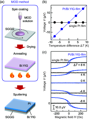
In Figs. 10(b) and 10(c), we respectively show the and dependences of in the Pt/Bi:YIG STE-coating film. The clear LSSE voltage was found to appear even in this thin film structure prepared by the MOD coating method. We also checked that no signal appears in a plain Pt film sputtered directly on a SGGG substrate, indicating that the thin Bi:YIG film works as a thermoelectric generator. We found that a crystalline Bi:YIG film can be grown even onto a glass substrate by using the MOD method SSE_Kirihara2012NatMat , and the STE coating is applicable even onto amorphous surfaces. Such versatile implementation of thermoelectric functions may open opportunities for various applications making full use of omnipresent heat.
V.2 Flexible spin Seebeck devices
Most of the conventional thermoelectric devices are rigid, and not easily applicable onto curved or uneven heat sources. Because the conventional thermoelectric device consists of a number of -structured thermocouples connected electrically in series, it is vulnerable to bending stresses, making it difficult to construct flexible devices. In contrast, the LSSE device has a high affinity for flexible thermoelectric generation owing to its simple structure and scaling law; it will be applicable on various heat sources, paving the way to versatile thermoelectric generators or sensors.
Recently, we demonstrated the construction of a LSSE-based flexible thermoelectric sheet SSE_Kirihara2015 . To construct the flexible LSSE device, we used spray-coating technique called “ferrite plating” Abe1992 ; Kondo2007 , which enables the fabrication of ferrimagnetic ferrite thin films. Since conventional ferrite-film preparation techniques, including sputtering SSE_Niizeki2015AIPAdv_CFO , liquid phase epitaxy Qiu_spin-pump_2013APL , and pulsed laser deposition spin mixing concept , require high temperature processes (ranging from 400 ∘C to 800 ∘C) for crystallizing ferrites, they cannot be used for the formation of ferrite films on heat-labile soft materials, such as plastics. By contrast, the ferrite plating method is based on chemical reaction processes, and thus does not need any high temperature processes, enabling the coating of ferrite films on a variety of substrates including flexible plastic films.
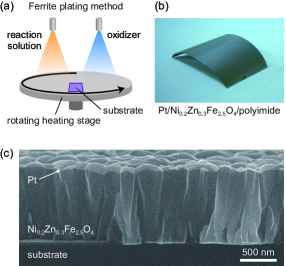
The fabrication process of the ferrite plating method is very simple, which also requires no specialized and costly equipment. As schematically illustrated in Fig. 11(a), the ferrite film can be grown simply by spraying an aqueous reaction solution and an oxidizer simultaneously onto a substrate, mounted on a rotating heating stage Abe1992 ; Kondo2007 . The thickness of the ferrite film can be controlled by the spray volume and time and can be dependent on surface conditions of substrates. Importantly, all the processes of the ferrite plating method can be performed below 100 ∘C, applicable to heat-labile plastic substrates.
By using the ferrite plating method, we successfully fabricated the flexible thermoelectric sheet based on the LSSE [see a photograph in Fig. 11(b)]. The flexible LSSE device consists of a ferrimagnetic Ni0.2Zn0.3Fe2.5O4 thin film, grown on a flexible polyimide substrate by the ferrite plating, and a Pt film, sputtered on the Ni0.2Zn0.3Fe2.5O4 film. As shown in Fig. 11(b), the Pt/Ni0.2Zn0.3Fe2.5O4/polyimide sheet is highly flexible and bendable. We observed clear LSSE signals in the flexible thermoelectric sheet, where the magnitude of the LSSE signals is comparable to that in the conventional rigid LSSE devices SSE_Kirihara2015 . We also demonstrated that the ferrite plating method is applicable to not only plastic substrates but also glass substrates; it is useful for constructing low-cost LSSE devices.
A noticeable feature of the ferrite film grown by the ferrite plating method is its columnar grain structure [see the cross-sectional scanning electron microscope image of the Ni0.2Zn0.3Fe2.5O4 film in Fig. 11(c)]. Here, the crystal orientation of Ni0.2Zn0.3Fe2.5O4 is coherently aligned within each columnar grain SSE_Kirihara2015 . Such columnar structure can be suitable for the flexible LSSE devices because of the following two reasons. First, in the LSSE configuration, the spin current is generated along the columnar structure, and thus less affected by grain scattering. Second, the columnar grain boundary can work as a stress-relieving cushion when the film is bent, leading to the high flexibility and bending tolerance.
The ferrite plating method potentially enables the direct coating of thermoelectric functions onto various surfaces over a large area, expanding the versatility and utility of the LSSE devices. Significantly, the flexible thermoelectric sheet based on the LSSE, demonstrated here, has remarkably low thermal resistance because of the thick-substrate-free structure. Therefore, it may be suitable for heat-flow sensing applications SSE_Kirihara2015 .
V.3 Hybrid thermoelectric generation based on spin Seebeck and anomalous Nernst effects
As shown in Fig. 2, most of the LSSE experiments to date have been performed by using Pt as a metallic layer. Pt is useful for investigating the physics of the LSSE, since it enables sensitive detection of the thermally generated spin currents and the spin-current-related parameters, such as the spin diffusion length and spin Hall angle, of Pt have been well studied ISHE_Sinova . However, Pt is unsuitable for thermoelectric applications of the LSSE because of its high material cost. Furthermore, even the spin-charge conversion efficiency of Pt is insufficient for obtaining adequate thermoelectric performance.
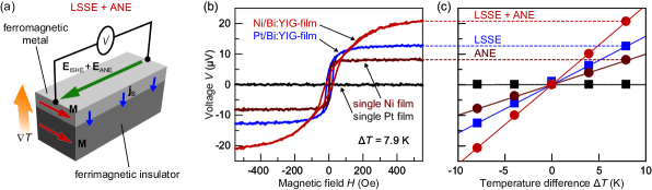
Recently, the ISHE has been investigated not only in paramagnetic materials but also in ferromagnetic materials by means of the LSSE experiments SSE_Miao2013PRL_PyYIG ; SSE_Kikkawa2013PRB ; SSE_Azevedo2014APL_PyYIG ; SSE_Wu2014APL_Fe3O4 ; SSE_Tian2015APL ; SSE_TSeki2015APL (Fig. 2). The main purpose of these studies is microscopic understanding of the ISHE in ferromagnets. In contrast, we focus on ferromagnetic materials as low-cost replacements for Pt in the LSSE devices. Here, as a simple model case, we consider a ferromagnetic metal/ferrimagnetic insulator junction system under a temperature gradient. In this system, the ANE is induced in the ferromagnetic metal layer in a conventional manner. In addition to the ANE contribution, if the spin current is injected into the ferromagnetic metal from the ferrimagnetic insulator via the LSSE and the ISHE appears in the ferromagnetic metal, the hybrid thermoelectric generation based on the combination of the LSSE and ANE is realized [Fig. 12(a)]. The previous studies showed that the direction of is the same as that of in various ferromagnetic materials SSE_Miao2013PRL_PyYIG ; SSE_Kikkawa2013PRB ; SSE_Azevedo2014APL_PyYIG ; SSE_Wu2014APL_Fe3O4 ; SSE_Tian2015APL ; SSE_TSeki2015APL . Even when the spin Hall angle of the ferromagnetic metal is smaller than that of Pt, the shortfall of the ISHE voltage can be compensated by the superposition of the ANE voltage. In fact, the thermoelectric output of all-ferromagnetic devices can even be better than that of the conventional Pt-based devices, as demonstrated below.
In Figs. 12(b) and 12(c), we compare the transverse thermoelectric voltage between ferromagnetic Ni/Bi:YIG-film and conventional Pt/Bi:YIG-film systems. The Bi:YIG layer of the Ni/Bi:YIG-film and Pt/Bi:YIG-film samples were formed on a SGGG substrate by means of the MOD method. We found that the Ni/Bi:YIG-film sample exhibits the clear signal of which the magnitude is more than twice greater than that of the ANE voltage in a plain Ni film directly placed on the substrate, indicating that the signal in the Ni/Bi:YIG-film sample is attributed to the superposition of the ANE in the Ni layer and the ISHE induced by the spin current injected from the Bi:YIG layer. Importantly, the magnitude of in the Ni/Bi:YIG-film sample is even greater than that in the conventional Pt/Bi:YIG-film sample [Figs. 12(b) and 12(c)]. Since the electrical resistivity of Ni is comparable to or smaller than that of Pt, the Ni/Bi:YIG-film sample shows the better thermoelectric performance than the Pt/Bi:YIG-film sample in terms of not only the output voltage but also the output current or power. This result suggests that the hybrid thermoelectric generation using ferromagnetic metal/ferrimagnetic insulator junction systems will be useful for constructing noble-metal-free, low-cost, and efficient LSSE devices.
V.4 Spin Seebeck effect in multilayer devices
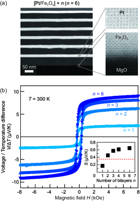
To realize efficient thermal spin-current generation, the LSSE has recently been investigated in multilayer systems comprising alternately-stacked paramagnet (P)/ferromagnet (F) films SSE_ML_Lee ; SSE_LSMO_La2NiMnO6 ; SSE_ML_Ramos . The recent studies have revealed that the LSSE voltage in [P/F] systems significantly and monotonically increases with increasing the number of the P/F bilayers . For example, in SSE_ML_Ramos , the magnitude of the LSSE voltage in [Pt/Fe3O4] 6 systems was observed to be enhanced by a factor of 4–6 compared with that in [Pt/Fe3O4] 1 bilayer systems (Fig. 13). Since this LSSE-voltage enhancement is unaccompanied by the increase of the internal resistance, the output power also increases with increasing , a situation different from the case of the LSSE-voltage enhancement by the spin Hall thermopile SSE-Uchida2014JPCM ; SSE_Uchida2012APEX . The observed dependence of the LSSE voltage in the [P/F] multilayer systems is beyond conventional expectations based on the situation that the systems are merely regarded as several independent P/F bilayers electrically connected in parallel, where the output voltage is not enhanced while the output power is enhanced owing to the reduction of the internal resistance [Fig. 14(a)] SSE_ML_Ramos . Importantly, this LSSE-voltage enhancement cannot be explained even when the spin-current injection into P from both the top and bottom F layers is taken into account, where the upper limit of the LSSE enhancement is twice of the voltage in the single P/F bilayer; as shown in Fig. 13(b), the observed enhancement is much greater than this upper limit.
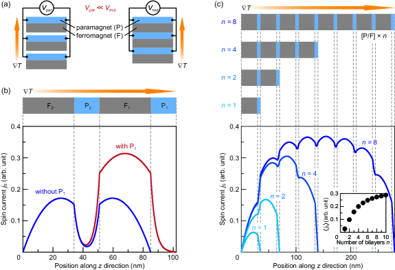
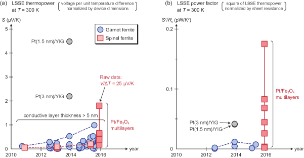
Our current interpretation of the mechanism of the LSSE enhancement in the P/F multilayer systems is summarized as follows SSE_ML_Ramos . The essence of the LSSE enhancement is the boundary conditions for spin currents flowing normal to the P/F interfaces, which affect the magnitude and spatial profile of the spin currents generated by the LSSE. Here we assume the following two boundary conditions: (i) spin currents must disappear at the top and bottom surfaces of the multilayer systems and (ii) spin currents in the P and F layers are continuous at the interfaces. Although spin currents in paramagnetic metals and ferrimagnetic insulators are respectively carried by conduction electrons and spin waves, the boundary condition (ii) allows us to treat these spin currents in the same manner in the following phenomenological discussions. Let us now compare a spin-current profile in a P1/F1/P2/F2 system with that in a F1/P2/F2 system without the top P layer (P1) [Fig. 14(b)], where P1 and P2 are good spin sinks. According to the boundary condition (i), the spin current is eliminated at the top of the F1 layer in the F1/P2/F2 system. However, this is not the case for the P1/F1/P2/F2 system; the spin current remains a large value at the P1/F1 interface, while it must disappear at the top of the P1 layer. As shown in Fig. 14(b), this difference results in the enhancement of the spin currents near the P1/F1 interface, a situation consistent with the prediction in SSE_Hoffman2013PRB . By applying the above discussion, we calculated out-of-plane spin-current profiles in the [P/F] systems for various values of [Fig. 14(c)] and the dependence of the spin-current magnitude averaged over all the P layers [the inset to Fig. 14(c)] (note that can be regarded as an observable quantity in the measurements of the LSSE in the P/F multilayer systems, since the P layers are electrically connected with each other due to the small thickness and resultant small out-of-plane electrical resistance of the F layers SSE_ML_Ramos ). Importantly, the magnitude of monotonically increases with increasing . The physics behind is that, thanks to the multilayer structure, the spin current in the P interlayers acquires a new length scale and boundary value. This phenomenological interpretation is consistent with the experimental results; similar dependence of the LSSE voltage was observed in the [Pt/Fe3O4] systems [compare the inset to Fig. 13(b) with that to Fig. 14(c)] SSE_ML_Ramos . The [Pt/Fe3O4] 6 system holds the current record of the LSSE thermopower at room temperature (Fig. 15). Since the enhancement of the LSSE based on this mechanism strongly depends on the spin diffusion length (magnon diffusion length) of the P (F) layer, the determination of optimum thicknesses of each layer and optimum P/F material combination is crucial for further improvement of the thermoelectric performance of the LSSE devices.
VI Conclusions and prospects
In this article, we reviewed the experimental results of the LSSE in insulator-based systems from the viewpoint of thermoelectric applications. The basic structure of the LSSE device is a simple bilayer film comprising a magnetic insulator and a metallic or other conductive material; an out-of-plane temperature gradient in the magnetic insulator layer induces an in-plane electric field in the metallic layer via spin-current generation across the interface. Owing to this configuration, the LSSE device exhibits the following unique characteristics. Firstly, the figure of merit of the LSSE device is free from the Wiedemann-Franz law, and can be optimized by selecting the combination of a magnetic insulator with low thermal conductivity and a metallic film with low electrical resistivity. Secondly, the LSSE device follows the convenient scaling law; the maximum extractable power of the LSSE device is proportional to the device area, and can be enhanced simply enlarging the device without constructing complicated modules. The simple structure and scaling law of the LSSE device make it possible to implement thermoelectric functions onto various heat sources by using versatile and low-cost fabrication processes.
The thermoelectric performance of the LSSE device cannot be simply compared with that of conventional thermoelectric devices based on the Seebeck effect because of the different device configurations and driving principles. The theory presented in Sec. IV shows that the thermoelectric conversion efficiency of the LSSE device is characterized by the figure of merit , described by Eq. (34). Here, is defined as proportional to the square of the LSSE thermopower and inversely proportional to the thermal conductivity of a magnetic insulator and electrical resistivity of a metallic film, which is similar to the case of the conventional thermoelectric devices. However, the figure of merit of the LSSE device is defined in the range of , which is a characteristic of transverse thermoelectric devices.
Despite the potential advantages of the LSSE device, the current stage of the SSE research is still far from realistic thermoelectric applications. This is mainly because the LSSE thermopower is very small at present, although there is plenty of scope for the performance improvement. The LSSE thermopower can be enhanced by improving the thermal spin-current generation efficiency in the magnetic insulator, spin Hall angle in the metallic layer, and spin mixing conductance at the metal/insulator interface. In fact, owing to the efforts after the discovery of the LSSE, the thermoelectric performance of the LSSE device is being improved, especially, in recent years with the advent of multilayer systems as shown in the time-series trends of the LSSE thermopower [Fig. 15(a)] and the LSSE power factor [Fig. 15(b)] in typical LSSE devices. Here, we define the LSSE power factor as the output power normalized by the applied temperature gradient and by the device area:
| (39) |
where () is the sheet resistance of the metallic layer of the LSSE device and we assume . Figure 15(b) emphasizes again that multilayer systems are useful for improving the output power of the LSSE device due to the combination of the voltage enhancement and internal resistance reduction. Nevertheless, since even the current record of the thermoelectric performance of the LSSE is still inadequate, continuous development of the LSSE-based thermoelectric technology is necessary. For realistic thermoelectric applications, the reduction of the thermal conductivity (electrical resistivity) of the insulator layer (metallic layer) for the improvement of and optimum thermal design for the stable and continuous operation of the LSSE device are also indispensable.
In the field of spintronics, in addition to the SSE, a variety of novel phenomena in which the interplay of spin and heat plays a crucial role were discovered spincaloritronics-Heremans ; spincaloritronics-Bauer . Some of the thermo-spin phenomena, such as spin-dependent Seebeck effects Slachter2010NatPhys ; Breton2011Nature , Seebeck effects in magnetic tunnel junctions Walter2011NatMater , and magnon-drag effects Costache2012NatMat , are also potentially applicable to thermoelectric generation in nano-structured spintronics devices. Furthermore, at low temperatures, giant thermopower was observed in transverse SSE devices comprising non-magnetic semiconductors Jaworski2012Nature . Although the origin of this giant thermoelectric effect is different from the SSE discussed in this article, it represents a great potential of spin-based thermoelectric technologies. However, these thermo-spin phenomena appear only in conductors; the utilization of insulators is an exclusive feature of the SSE-based thermoelectric generation. We anticipate that this unique feature of the SSE will lead to various thermoelectric applications, including energy harvesters, thermometers, infrared sensors, position detectors SSE-Uchida2011JJAP , and user-interface devices.
ACKNOWLEDGMENTS
The authors thank M. H. Aguirre, M. Akimoto, P. A. Algarabel, A. Anadón, J. Barker, G. E. W. Bauer, S. R. Boona, C. L. Chien, S. Daimon, S. T. B. Goennenwein, J. P. Heremans, B. Hillebrands, T. Hioki, D. Hou, S. Y. Huang, M. R. Ibarra, J. Ieda, R. Iguchi, K. Ihara, Y. Iwasaki, H. Jin, X. F. Jin, D. Kikuchi, M. Kläui, S. Kohmoto, K. Kondo, I. Lucas, T. Manako, A. Matsuba, A. Miura, L. Morellón, T. Murakami, R. C. Myers, Y. Nakamura, T. Niizeki, T. Nonaka, J. Ohe, Y. Ohnuma, Y. Oikawa, T. Ota, T. Oyake, Z. Qiu, R. Ramos, S. M. Rezende, K. Sato, T. Seki, J. Shiomi, Y. Shiomi, H. Someya, S. Takahashi, K. Takanashi, Y. Tserkovnyak, B. J. van Wees, J. Xiao, N. Yamamoto, and A. Yagmur for valuable discussions.
This work was supported by PRESTO “Phase Interfaces for Highly Efficient Energy Utilization” from JST, Japan, Grant-in-Aid for Scientific Research (A) (No. 15H02012), Grant-in-Aid for Challenging Exploratory Research (No. 26600067), Grant-in-Aid for Scientific Research on Innovative Area, “Nano Spin Conversion Science” (No. 26103005) from MEXT, Japan, and NEC Corporation. T.K. is supported by JSPS through a research fellowship for young scientists (No. 15J08026).
References
- (1) F. J. DiSalvo, “Thermoelectric cooling and power generation,” Science, vol. 285, no. 5428, pp. 703-706, Jul. 1999.
- (2) L. E. Bell, “Cooling, heating, generating power, and recovering waste heat with thermoelectric systems,” Science, vol. 321, no. 5895, pp. 1457-1461, Sep. 2008.
- (3) P. Sundarraj, D. Maity, S. S. Roy, and R. A. Taylor, “Recent advances in thermoelectric materials and solar thermoelectric generators - a critical review,” RSC Adv., vol. 4, no. 87, pp. 46860-46874, Sep. 2014.
- (4) D. M. Rowe ed., CRC Handbook of Thermoelectrics. CRC Press, 1995.
- (5) H. J. Goldsmid, Introduction to Thermoelectricity. Springer, 2009.
- (6) S. R. Boona, R. C. Myers, and J. P. Heremans, “Spin caloritronics,” Energy Environ. Sci., vol. 7, no. 3, pp. 885-910, Mar. 2014.
- (7) L.-D. Zhao, S.-H. Lo, Y. Zhang, H. Sun, G. Tan, C. Uher, C. Wolverton, V. P. Dravid, and M. G. Kanatzidis, “Ultralow thermal conductivity and high thermoelectric figure of merit in SnSe crystals,” Nature, vol. 508, no. 7496, pp. 373-377, Apr. 2014.
- (8) J. P. Heremans, “Thermoelectricity: The ugly duckling,” Nature, vol. 508, no. 7496, pp. 327-328, Apr. 2014.
- (9) L. D. Hicks and M. S. Dresselhaus, “Effect of quantum-well structures on the thermoelectric figure of merit,” Phys. Rev. B, vol. 47, no. 19, pp. 12727-12731, May 1993.
- (10) A. I. Hochbaum, R. Chen, R. D. Delgado, W. Liang, E. C. Garnett, M. Najarian, A. Majumdar, and P. Yang, “Enhanced thermoelectric performance of rough silicon nanowires,” Nature, vol. 451, no. 7175, pp. 163-167, Jan. 2008.
- (11) B. Poudel, Q. Hao, Y. Ma, Y. Lan, A. Minnich, B. Yu, X. Yan, D. Wang, A. Muto, D. Vashaee, X. Chen, J. Liu, M. S. Dresselhaus, G. Chen, and Z. Ren, “High-thermoelectric performance of nanostructured bismuth antimony telluride bulk alloys,” Science, vol. 320, no. 5876, pp. 634-638, May 2008.
- (12) A. J. Minnich, M. S. Dresselhaus, Z. F. Ren, and G. Chen, “Bulk nanostructured thermoelectric materials: current research and future prospects,” Energy Environ. Sci., vol. 2, no. 5, pp. 466-479, May 2009.
- (13) J.-F. Li, W.-S. Liu, L.-D. Zhao, and M. Zhou, “High-performance nanostructured thermoelectric materials,” NPG Asia Mater., vol. 2, no. 4, pp. 152-158, Oct. 2010.
- (14) P. E. Hopkins, C. M. Reinke, M. F. Su, R. H. Olsson, III, E. A. Shaner, Z. C. Leseman, J. R. Serrano, L. M. Phinney, and I. El-Kady, “Reduction in the thermal conductivity of single crystalline silicon by phononic crystal patterning,” Nano Lett., vol. 11, no. 1, pp. 107-112, Jan 2011.
- (15) M. Kashiwagi, S. Hirata, K. Harada, Y. Zheng, K. Miyazaki, M. Yahiro, and C. Adachi, “Enhanced figure of merit of a porous thin film of bismuth antimony telluride,” Appl. Phys. Lett., vol. 98, no. 2, pp. 023114/1-023114/3, Jan. 2011.
- (16) J. Maire and M. Nomura, “Reduced thermal conductivities of Si one-dimensional periodic structure and nanowire,” Jpn. J. Appl. Phys., vol. 53, no. 6S, pp. 06JE09/1-06JE09/4, Jun. 2014.
- (17) A. Miura, S. Zhou, T. Nozaki, and J. Shiomi, “Crystalline-amorphous silicon nanocomposites with reduced thermal conductivity for bulk thermoelectrics,” ACS Appl. Mater. Interfaces, vol. 7, no. 24, pp. 13484-13489, Jun. 2015.
- (18) D. T. Morelli, J. Heremans, M. Sakamoto, and C. Uher, “Anisotropic heat conduction in diacetylenes,” Phys. Rev. Lett., vol. 57, no. 7, pp. 869-872, Aug. 1986.
- (19) A. A. Balandin, “Thermal properties of graphene and nanostructured carbon materials,” Nature Mater., vol. 10, no. 8, pp. 569-581, Aug. 2011.
- (20) J. L. Cohn, B. D. White, C. A. M. dos Santos, and J. J. Neumeier, “Giant Nernst effect and bipolarity in the quasi-one-dimensional metal Li0.9Mo6O17,” Phys. Rev. Lett., vol. 108, no. 5, pp. 056604/1-056604/5, Feb. 2012.
- (21) S. Z. Butler, S. M. Hollen, L. Cao, Y. Cui, J. A. Gupta, H. R. Gutiérrez, T. F. Heinz, S. S. Hong, J. Huang, A. F. Ismach, E. Johnston-Halperin, M. Kuno, V. V. Plashnitsa, R. D. Robinson, R. S. Ruoff, S. Salahuddin, J. Shan, L. Shi, M. G. Spencer, M. Terrones, W. Windl, and J. E. Goldberger, “Progress, challenges, and opportunities in two-dimensional materials beyond graphene,” ACS NANO, vol. 7, no. 4, pp. 2898-2926, Apr. 2013.
- (22) R. Fei, A. Faghaninia, R. Soklaski, J.-A. Yan, C. Lo, and L. Yang, “Enhanced thermoelectric efficiency via orthogonal electrical and thermal conductances in phosphorene,” Nano Lett., vol. 14, no. 11, pp. 6393-6399, Nov. 2014.
- (23) S. A. Wolf, D. D. Awschalom, R. A. Buhrman, J. M. Daughton, S. von Molnár, M. L. Roukes, A. Y. Chtchelkanova, and D. M. Treger, “Spintronics: A spin-based electronics vision for the future,” Science, vol. 294, no. 5546, pp. 1488-1495, Nov. 2001.
- (24) I. Žutić, J. Fabian, and S. Das Sarma, “Spintronics: Fundamentals and applications,” Rev. Mod. Phys., vol. 76, no. 2, pp. 323-410, Apr. 2004.
- (25) G. E. W. Bauer, E. Saitoh, and B. J. van Wees, “Spin caloritronics,” Nature Mater., vol. 11, no. 5, pp. 391-399, May 2012.
- (26) K. Uchida, S. Takahashi, K. Harii, J. Ieda, W. Koshibae, K. Ando, S. Maekawa, and E. Saitoh, “Observation of the spin Seebeck effect,” Nature, vol. 455, no. 7214, pp. 778-781, Oct. 2008.
- (27) S. Maekawa, E. Saitoh, S. O. Valenzuela, and T. Kimura eds., Spin Current. Oxford University Press, Oxford, 2012.
- (28) S. Maekawa, H. Adachi, K. Uchida, J. Ieda, and E. Saitoh, “Spin current: Experimental and theoretical aspects,” J. Phys. Soc. Japan, vol. 82, no. 10, pp. 102002/1-102002/23, Oct. 2013.
- (29) A. Azevedo, L. H. Vilela-Leão, R. L. Rodríguez-Suárez, A. B. Oliveira, and S. M. Rezende, “dc effect in ferromagnetic resonance: Evidence of the spin-pumping effect?,” J. Appl. Phys., vol. 97, no. 10, pp. 10C715/1-10C715/3, May 2005.
- (30) E. Saitoh, M. Ueda, H. Miyajima, and G. Tatara, “Conversion of spin current into charge current at room temperature: Inverse spin-Hall effect,” Appl. Phys. Lett., vol. 88, no. 18, pp. 182509/1-182509/3, May 2006.
- (31) S. O. Valenzuela and M. Tinkham, “Direct electronic measurement of the spin Hall effect,” Nature, vol. 442, no. 7099, pp. 176-179, Jul. 2006.
- (32) M. V. Costache, M. Sladkov, S. M. Watts, C. H. van der Wal, and B. J. van Wees, “Electrical detection of spin pumping due to the precessing magnetization of a single ferromagnet,” Phys. Rev. Lett., vol. 97, no. 21, pp. 216603/1-216603/4, Nov. 2006.
- (33) T. Kimura, Y. Otani, T. Sato, S. Takahashi, and S. Maekawa, “Room-temperature reversible spin Hall effect,” Phys. Rev. Lett., vol. 98, no. 15, pp. 156601/1-156601/4, Apr. 2007.
- (34) J. Sinova, S. O. Valenzuela, J. Wunderlich, C. H. Back, and T. Jungwirth, “Spin Hall effects,” Rev. Mod. Phys., vol. 87, no. 4, pp. 1213-1259, Oct. 2015.
- (35) K. Uchida, T. Ota, K. Harii, K. Ando, H. Nakayama, and E. Saitoh, “Electric detection of the spin-Seebeck effect in ferromagnetic metals,” J. Appl. Phys., vol. 107, no. 9, pp. 09A951/1-09A951/5, May 2010.
- (36) S. Bosu, Y. Sakuraba, K. Uchida, K. Saito, T. Ota, E. Saitoh, and K. Takanashi, “Spin Seebeck effect in thin films of the Heusler compound Co2MnSi,” Phys. Rev. B, vol. 83, no. 22, pp. 224401/1-22440/6, Jun. 2011.
- (37) K. Uchida, H. Adachi, T. An, T. Ota, M. Toda, B. Hillebrands, S. Maekawa, and E. Saitoh, “Long-range spin Seebeck effect and acoustic spin pumping,” Nature Mater., vol. 10, no. 10, pp. 737-741, Oct. 2011.
- (38) S. H. Wang, L. K. Zou, J. W. Cai, B. G. Shen, and J. R. Sun, “Transverse thermoelectric effects in platinum strips on permalloy films,” Phys. Rev. B, vol. 88, no. 21, pp. 214304/1-214304/6, Dec. 2013.
- (39) C. M. Jaworski, J. Yang, S. Mack, D. D. Awschalom, J. P. Heremans, and R. C. Myers, “Observation of the spin-Seebeck effect in a ferromagnetic semiconductor,” Nature Mater., vol. 9, no. 11, pp. 898-903, Nov. 2010.
- (40) C. M. Jaworski, J. Yang, S. Mack, D. D. Awschalom, R. C. Myers, and J. P. Heremans, “Spin-Seebeck effect: A phonon driven spin distribution,” Phys. Rev. Lett., vol. 106, no. 18, pp. 186601/1-186601/4, May 2011.
- (41) K. Uchida, J. Xiao, H. Adachi, J. Ohe, S. Takahashi, J. Ieda, T. Ota, Y. Kajiwara, H. Umezawa, H. Kawai, G. E. W. Bauer, S. Maekawa, and E. Saitoh, “Spin Seebeck insulator,” Nature Mater., vol. 9, no. 11, pp. 894-897, Nov. 2010.
- (42) K. Uchida, H. Adachi, T. Ota, H. Nakayama, S. Maekawa, and E. Saitoh, “Observation of longitudinal spin-Seebeck effect in magnetic insulators,” Appl. Phys. Lett., vol. 97, no. 17, pp. 172505/1-172505/3, Oct. 2010.
- (43) A. Kirihara, K. Uchida, Y. Kajiwara, M. Ishida, Y. Nakamura, T. Manako, E. Saitoh, and S. Yorozu, “Spin-current-driven thermoelectric coating,” Nature Mater., vol. 11, no. 8, pp. 686-689, Aug. 2012.
- (44) K. Uchida, M. Ishida, T. Kikkawa, A. Kirihara, T. Murakami, and E. Saitoh, “Longitudinal spin Seebeck effect: from fundamentals to applications,” J. Phys.: Condens. Matter, vol. 26, no. 34, pp. 343202/1-343202/15, Aug. 2014.
- (45) K. Uchida, T. Ota, H. Adachi, J. Xiao, T. Nonaka, Y. Kajiwara, G. E. W. Bauer, S. Maekawa, and E. Saitoh, “Thermal spin pumping and magnon-phonon-mediated spin-Seebeck effect,” J. Appl. Phys., vol. 111, no. 10, pp. 103903/1-103903/12, May 2012.
- (46) K. Uchida, T. Nonaka, T. Ota, and E. Saitoh, “Longitudinal spin-Seebeck effect in sintered polycrystalline (Mn, Zn)Fe2O4,” Appl. Phys. Lett., vol. 97, no. 26, pp. 262504/1-262504/3, Dec. 2010.
- (47) K. Uchida, A. Kirihara, M. Ishida, R. Takahashi, and E. Saitoh, “Local spin-Seebeck effect enabling two-dimensional position sensing,” Jpn. J. Appl. Phys., vol. 50, no. 12R, pp. 120211/1-120211/3, Dec. 2011.
- (48) M. Weiler, M. Althammer, F. D. Czeschka, H. Huebl, M. S. Wagner, M. Opel, I.-M. Imort, G. Reiss, A. Thomas, R. Gross, and S. T. B. Goennenwein, “Local charge and spin currents in magnetothermal landscapes,” Phys. Rev. Lett., vol. 108, no. 10, pp. 106602/1-106602/5, Mar. 2012.
- (49) K. Uchida, T. Nonaka, T. Yoshino, T. Kikkawa, D. Kikuchi, and E. Saitoh, “Enhancement of spin-Seebeck voltage by spin-Hall thermopile,” Appl. Phys. Express, vol. 5, no. 9, pp. 093001/1-093001/3, Sep. 2012.
- (50) D. Qu, S. Y. Huang, J. Hu, R. Wu, and C. L. Chien, “Intrinsic spin Seebeck effect in Au/YIG,” Phys. Rev. Lett., vol. 110, no. 6, pp. 067206/1-067206/5, Feb. 2013.
- (51) T. Kikkawa, K. Uchida, Y. Shiomi, Z. Qiu, D. Hou, D. Tian, H. Nakayama, X.-F. Jin, and E. Saitoh, “Longitudinal spin Seebeck effect free from the proximity Nernst effect,” Phys. Rev. Lett., vol. 110, no. 6, pp. 067207/1-067207/5, Feb. 2013.
- (52) M. B. Jungfleisch, T. An, K. Ando, Y. Kajiwara, K. Uchida, V. I. Vasyuchka, A. V. Chumak, A. A. Serga, E. Saitoh, and B. Hillebrands, “Heat-induced damping modification in yttrium iron garnet/platinum hetero-structures,” Appl. Phys. Lett., vol. 102, no. 6, pp. 062417/1-062417/4, Feb. 2013.
- (53) D. Meier, T. Kuschel, L. Shen, A. Gupta, T. Kikkawa, K. Uchida, E. Saitoh, J.-M. Schmalhorst, and G. Reiss, “Thermally driven spin and charge currents in thin NiFe2O4/Pt films,” Phys. Rev. B, vol. 87, no. 5, pp. 054421/1-054421/5, Feb. 2013.
- (54) R. Ramos , T. Kikkawa, K. Uchida, H. Adachi, I. Lucas, M. H. Aguirre, P. Algarabel, L. Morellón, S. Maekawa, E. Saitoh, and M. R. Ibarra, “Observation of the spin Seebeck effect in epitaxial Fe3O4 thin films,” Appl. Phys. Lett., vol. 102, no. 7, pp. 072413/1-072413/5, Feb. 2013.
- (55) K. Uchida, T. Nonaka, T. Kikkawa, Y. Kajiwara, and E. Saitoh, “Longitudinal spin Seebeck effect in various garnet ferrites,” Phys. Rev. B, vol. 87, no. 10, pp. 104412/1-104412/6, Mar. 2013.
- (56) B. F. Miao, S. Y. Huang, D. Qu, and C. L. Chien, “Inverse spin Hall effect in a ferromagnetic metal,” Phys. Rev. Lett., vol. 111, no. 6, pp. 066602/1-066602/5, Aug. 2013.
- (57) M. Schreier, A. Kamra, M. Weiler, J. Xiao, G. E. W. Bauer, R. Gross, and S. T. B. Goennenwein, “Magnon, phonon, and electron temperature profiles and the spin Seebeck effect in magnetic insulator/normal metal hybrid structures,” Phys. Rev. B, vol. 88, no. 9, pp. 094410/1-094410/13, Sep. 2013.
- (58) T. Kikkawa, K. Uchida, S. Daimon, Y. Shiomi, H. Adachi, Z. Qiu, D. Hou, X.-F. Jin, S. Maekawa, and E. Saitoh, “Separation of longitudinal spin Seebeck effect from anomalous Nernst effect: Determination of origin of transverse thermoelectric voltage in metal/insulator junctions,” Phys. Rev. B, vol. 88, no. 21, pp. 214403/1-214403/11, Dec. 2013.
- (59) M. Schreier, N. Roschewsky, E. Dobler, S. Meyer, H. Huebl, R. Gross, and S. T. B. Goennenwein, “Current heating induced spin Seebeck effect,” Appl. Phys. Lett., vol. 103, no. 24, pp. 242404/1-242404/4, Dec. 2013.
- (60) S. M. Rezende, R. L. Rodríguez-Suárez, R. O. Cunha, A. R. Rodrigues, F. L. A. Machado, G. A. Fonseca Guerra, J. C. Lopez Ortiz, and A. Azevedo, “Magnon spin-current theory for the longitudinal spin-Seebeck effect,” Phys. Rev. B, vol. 89, no. 1, pp. 014416/1-014416/10, Jan. 2014.
- (61) A. Azevedo, O. Alves Santos, G. A. Fonseca Guerra, R. O. Cunha, R. Rodríguez-Suárez, and S. M. Rezende, “Competing spin pumping effects in magnetic hybrid structures,” Appl. Phys. Lett., vol. 104, no. 5, pp. 052402/1-052402/5, Feb. 2014.
- (62) G. Siegel, M. C. Prestgard, S. Teng, and A. Tiwari, “Robust longitudinal spin-Seebeck effect in Bi-YIG thin films,” Sci. Rep., vol. 4, pp. 4429/1-4429/6, Mar. 2014.
- (63) J. B. S. Mendes, R. O. Cunha, O. Alves Santos, P. R. T. Ribeiro, F. L. A. Machado, R. L. Rodríguez-Suárez, A. Azevedo, and S. M. Rezende, “Large inverse spin Hall effect in the antiferromagnetic metal Ir20Mn80,” Phys. Rev. B, vol. 89, no. 14, pp. 140406(R)/1-140406(R)/5, Apr. 2014.
- (64) D. Qu, S. Y. Huang, B. F. Miao, S. X. Huang, and C. L. Chien, “Self-consistent determination of spin Hall angles in selected 5 metals by thermal spin injection,” Phys. Rev. B, vol. 89, no. 14, pp. 140407(R)/1-140407(R)/5, Apr. 2014.
- (65) A. Kehlberger, G. Jakob, M. C. Onbasli, D. H. Kim, C. A. Ross, and M. Kläui, “Investigation of the magnetic properties of insulating thin films using the longitudinal spin Seebeck effect,” J. Appl. Phys., vol. 115, no. 17, pp. 17C731/1-17C731/3, May 2014.
- (66) N. Roschewsky, M. Schreier, A. Kamra, F. Schade, K. Ganzhorn, S. Meyer, H. Huebl, S. Geprägs, R. Gross, and S. T. B. Goennenwein, “Time resolved spin Seebeck effect experiments,” Appl. Phys. Lett., vol. 104, no. 20, pp. 202410/1-202410/4, May 2014.
- (67) M. Agrawal, V. I. Vasyuchka, A. A. Serga, A. Kirihara, P. Pirro, T. Langner, M. B. Jungfleisch, A. V. Chumak, E. Th. Papaioannou, and B. Hillebrands, “Role of bulk-magnon transport in the temporal evolution of the longitudinal spin-Seebeck effect,” Phys. Rev. B, vol. 89, no. 22, pp. 224414/1-224414/5, Jun. 2014.
- (68) M. Agrawal, A. A. Serga, V. Lauer, E. Th. Papaioannou, B. Hillebrands, and V. I. Vasyuchka, “Microwave-induced spin currents in ferromagnetic-insulatornormal metal bilayer system,” Appl. Phys. Lett., vol. 105, no. 9, pp. 092404/1-092404/4, Sep. 2014.
- (69) Y. Saiga, K. Mizunuma, Y. Kono, J. C. Ryu, H. Ono, M. Kohda, and E. Okuno, “Platinum thickness dependence and annealing effect of the spin-Seebeck voltage in platinum/yttrium iron garnet structures,” Appl. Phys. Express, vol. 7, no. 9, pp. 093001/1-093001/4, Sep. 2014.
- (70) S. M. Wu, J. Hoffman, J. E. Pearson, and A. Bhattacharya, “Unambiguous separation of the inverse spin Hall and anomalous Nernst effects within a ferromagnetic metal using the spin Seebeck effect,” Appl. Phys. Lett., vol. 105, no. 9, pp. 092409/1-092409/4, Sep. 2014.
- (71) J. Lustikova, Y. Shiomi, Z. Qiu, T. Kikkawa, R. Iguchi, K. Uchida, and E. Saitoh, “Spin current generation from sputtered Y3Fe5O12 films,” J. Appl. Phys., vol. 116, no. 15, pp. 153902/1-153902/6, Oct. 2014.
- (72) A. Aqeel, I. J. Vera-Marun, B. J. van Wees, and T. T. M. Palstra, “Surface sensitivity of the spin Seebeck effect,” J. Appl. Phys., vol. 116, no. 15, pp. 153705/1-153705/5, Oct. 2014.
- (73) W. X. Wang, S. H. Wang, L. K. Zou, J. W. Cai, Z. G. Sun, and J. R. Sun, “Joule heating-induced coexisted spin Seebeck effect and spin Hall magnetoresistance in the platinum/Y3Fe5O12 structure,” Appl. Phys. Lett., vol. 105, no. 18, pp. 182403/1-182403/5, Nov. 2014.
- (74) K. Uchida, T. Kikkawa, A. Miura, J. Shiomi, and E. Saitoh, “Quantitative temperature dependence of longitudinal spin Seebeck effect at high temperatures,” Phys. Rev. X, vol. 4, no. 4, pp. 041023/1-041023/9, Nov. 2014.
- (75) N. Vlietstra, J. Shan, B. J. van Wees, M. Isasa, F. Casanova, and J. Ben Youssef, “Simultaneous detection of the spin-Hall magnetoresistance and the spin-Seebeck effect in platinum and tantalum on yttrium iron garnet,” Phys. Rev. B, vol. 90, no. 17, pp. 174436/1-174436/8, Nov. 2014.
- (76) Y. Xu, B. Yang, C. Tang, Z. Jiang, M. Schneider, R. Whig, and J. Shi, “Heat-driven spin transport in a ferromagnetic metal,” Appl. Phys. Lett., vol. 105, no. 24, pp. 242404/1-242404/4, Dec. 2014.
- (77) P. Li, D. Ellsworth, H. Chang, P. Janantha, D. Richardson, F. Shah, P. Phillips, T. Vijayasarathy, and M. Wu, “Generation of pure spin currents via spin Seebeck effect in self-biased hexagonal ferrite thin films,” Appl. Phys. Lett., vol. 105, no. 24, pp. 242412/1-242412/4, Dec. 2014.
- (78) Y. Shiomi and E. Saitoh, “Paramagnetic spin pumping,” Phys. Rev. Lett., vol. 113, no. 26, pp. 266602/1-266602/5, Dec. 2014.
- (79) M. Schreier, G. E. W. Bauer, V. I. Vasyuchka, J. Flipse, K. Uchida, J. Lotze, V. Lauer, A. V. Chumak, A. A. Serga, S. Daimon, T. Kikkawa, E. Saitoh, B. J. van Wees, B. Hillebrands, R. Gross, and S. T. B. Goennenwein, “Sign of inverse spin Hall voltages generated by ferromagnetic resonance and temperature gradients in yttrium iron garnet platinum bilayers,” J. Phys. D: Appl. Phys., vol. 48, no. 2, 025001/1-025001/5, Jan. 2015.
- (80) D. Kikuchi, M. Ishida, K. Uchida, Z. Qiu, T. Murakami, and E. Saitoh, “Enhancement of spin-Seebeck effect by inserting ultra-thin Fe70Cu30 interlayer,” Appl. Phys. Lett., vol. 106, no. 8, pp. 082401/1-082401/4, Feb. 2015.
- (81) Z. Qiu, D. Hou, K. Uchida, and E. Saitoh, “Influence of interface condition on spin-Seebeck effects,” J. Phys. D: Appl. Phys., vol. 48, no. 16, pp. 164013/1-164013/5, Apr. 2015.
- (82) S. M. Wu, F. Y. Fradin, J. Hoffman, A. Hoffmann, and A. Bhattacharya, “Spin Seebeck devices using local on-chip heating,” J. Appl. Phys., vol. 117, pp. 17C509/1-17C509/4, May 2015.
- (83) A. Sola, M. Kuepferling, V. Basso, M. Pasquale, T. Kikkawa, K. Uchida, and E. Saitoh, “Evaluation of thermal gradients in longitudinal spin Seebeck effect measurements,” J. Appl. Phys., vol. 117, no. 17, pp. 17C510/1-17C510/4, May 2015.
- (84) H. Asada, A. Kuwahara, N. Sakata, T. Ono, T. Ishibashi, A. Meguro, T. Hashinaka, K. Kishimoto, and T. Koyanagi, “Longitudinal spin Seebeck effect in Nd2BiFe5-xGaxO12 prepared on gadolinium gallium garnet (001) by metal organic decomposition method,” J. Appl. Phys., vol. 117, no. 17, pp. 17C724/1-17C724/3, May 2015.
- (85) T. Niizeki, T. Kikkawa, K. Uchida, M. Oka, K. Z. Suzuki, H. Yanagihara, E. Kita, and E. Saitoh, “Observation of longitudinal spin-Seebeck effect in cobalt-ferrite epitaxial thin films,” AIP Adv., vol. 5, no. 5, pp. 053603/1-053603/6, May 2015.
- (86) S. M. Wu, J. E. Pearson, and A. Bhattacharya, “Paramagnetic spin Seebeck effect,” Phys. Rev. Lett., vol. 114, no. 18, pp. 186602/1-186602/5, May 2015.
- (87) D. Tian, Y. Li, D. Qu, X.-F. Jin, and C. L. Chien, “Separation of spin Seebeck effect and anomalous Nernst effect in Co/Cu/YIG,” Appl. Phys. Lett, vol. 106, no. 21, pp. 212407/1-212407/4, May 2015.
- (88) K.-D. Lee, D.-J. Kim, H. Y. Lee, S.-H. Kim, J.-H. Lee, K.-M. Lee, J.-R. Jeong, K.-S. Lee, H.-S. Song, J.-W. Sohn, S.-C. Shin, and B.-G. Park, “Thermoelectric signal enhancement by reconciling the spin Seebeck and anomalous Nernst effects in ferromagnet/non-magnet multilayers,” Sci. Rep., vol. 5, pp. 10249/1-10249/10, May 2015.
- (89) Y. Shiomi, Y. Handa, T. Kikkawa, and E. Saitoh, “Transverse thermoelectric effect in La0.67Sr0.33MnO3|SrRuO3 superlattices,” Appl. Phys. Lett., vol. 106, no. 23, pp. 232403/1-232403/4, Jun. 2015.
- (90) K. Uchida, J. Ohe, T. Kikkawa, S. Daimon, D. Hou, Z. Qiu, and E. Saitoh, “Intrinsic surface magnetic anisotropy in Y3Fe5O12 as the origin of low-magnetic-field behavior of the spin Seebeck effect,” Phys. Rev. B, vol. 92, no. 1, pp. 014415/1-014415/8, Jul. 2015.
- (91) D. Qu, S. Y. Huang, and C. L. Chien, “Inverse spin Hall effect in Cr: Independence of antiferromagnetic ordering,” Phys. Rev. B, vol. 92, no. 2, pp. 020418(R)/1-020418(R)/4, Jul. 2015.
- (92) Z. Qiu, D. Hou, T. Kikkawa, K. Uchida, and E. Saitoh, “All-oxide spin Seebeck effects,” Appl. Phys. Express, vol. 8, no. 8, pp. 083001/1-083001/3, Aug. 2015.
- (93) T. Kikkawa, K. Uchida, S. Daimon, Z. Qiu, Y. Shiomi, and E. Saitoh, “Critical suppression of spin Seebeck effect by magnetic fields,” Phys. Rev. B, vol. 92, no. 6, pp. 064413/1-064413/9, Aug. 2015.
- (94) H. Jin, S. R. Boona, Z. Yang, R. C. Myers, and J. P. Heremans, “Effect of the magnon dispersion on the longitudinal spin Seebeck effect in yttrium iron garnets,” Phys. Rev. B, vol. 92, no. 5, pp. 054436/1-054436/8, Aug. 2015.
- (95) A. Kehlberger, U. Ritzmann, D. Hinzke, E.-J. Guo, J. Cramer, G. Jakob, M. C. Onbasli, D. H. Kim, C. A. Ross, M. B. Jungfleisch, B. Hillebrands, U. Nowak, and M. Kläui, “Length scale of the spin Seebeck effect,” Phys. Rev. Lett., vol. 115, no. 9, pp. 096602/1-096602/5, Aug. 2015.
- (96) T. Seki, K. Uchida, T. Kikkawa, Z. Qiu, E. Saitoh, and K. Takanashi, “Observation of inverse spin Hall effect in ferromagnetic FePt alloys using spin Seebeck effect,” Appl. Phys. Lett., vol. 107, no. 9, pp. 092401/1-092401/4, Aug. 2015.
- (97) S. Wang, L. Zou, X. Zhang, J. Cai, S. Wang, B. Shen, and J. Sun, “Spin Seebeck effect and spin Hall magnetoresistance at high temperatures for a Pt/yttrium iron garnet hybrid structure,” Nanoscale, vol. 7, no. 42, pp. 17812-17819, Nov. 2015.
- (98) U. Ritzmann, D. Hinzke, A. Kehlberger, E.-J. Guo, M. Kläui, and U. Nowak, “Magnetic field control of the spin Seebeck effect,” Phys. Rev. B, vol. 92, no. 17, pp. 174411/1-174411/5, Nov. 2015.
- (99) A. Aqeel, N. Vlietstra, J. A. Heuver, G. E. W. Bauer, B. Noheda, B. J. van Wees, and T. T. M. Palstra, “Spin-Hall magnetoresistance and spin Seebeck effect in spin-spiral and paramagnetic phases of multiferroic CoCr2O4 films,” Phys. Rev. B, vol. 92, no. 22, pp. 224410/1-224410/8, Dec. 2015.
- (100) R. Ramos, T. Kikkawa, M. H. Aguirre, I. Lucas, A. Anadón, T. Oyake, K. Uchida, H. Adachi, J. Shiomi, P. A. Algarabel, L. Morellón, S. Maekawa, E. Saitoh, and M. R. Ibarra, “Unconventional scaling and significant enhancement of the spin Seebeck effect in multilayers,” Phys. Rev. B, vol. 92, no. 22, pp. 220407(R)/1-220407(R)/5, Dec. 2015.
- (101) A. Kirihara, M. Ishida, K. Uchida, H. Someya, Y. Iwasaki, K. Ihara, S. Kohmoto, E. Saitoh, and T. Murakami, “Spin-Seebeck thermoelectric converter,” IEEE International Nanoelectronics Conference, no. 7460433, pp. 1-3, July 2014.
- (102) S. Geprägs, A. Kehlberger, F. D. Coletta, Z. Qiu, E.-J. Guo, T. Schulz, C. Mix, S. Meyer, A. Kamra, M. Althammer, H. Huebl, G. Jakob, Y. Ohnuma, H. Adachi, J. Barker, S. Maekawa, G. E. W. Bauer, E. Saitoh, R. Gross, S. T. B. Goennenwein, and M. Kläui, “Origin of the spin Seebeck effect in compensated ferrimagnets,” Nature Commun., vol. 7, pp. 10452/1-10452/6, Feb. 2016.
- (103) E.-J. Guo, A. Kehlberger, J. Cramer, G. Jakob, and M. Kläui, “Origin of the thickness-dependent low-temperature enhancement of spin Seebeck effect in YIG films,” 2015. [Online]. Available: http://arxiv.org/abs/1506.06037
- (104) S. Seki, T. Ideue, M. Kubota, Y. Kozuka, R. Takagi, M. Nakamura, Y. Kaneko, M. Kawasaki, and Y. Tokura, “Thermal generation of spin current in an antiferromagnet,” Phys. Rev. Lett., vol. 115, no. 26, pp. 266601/1-266601/5, Dec. 2015.
- (105) S. M. Wu, W. Zhang, A. KC, P. Borisov, J. E. Pearson, J. S. Jiang, D. Lederman, A. Hoffmann, and A. Bhattacharya, “Antiferromagnetic spin Seebeck effect,” Phys. Rev. Lett., vol. 116, no. 9, pp. 097204/1-097204/5, Mar. 2016.
- (106) A. Kirihara, K. Kondo, M. Ishida, K. Ihara, Y. Iwasaki, H. Someya, A. Matsuba, K. Uchida, E. Saitoh, N. Yamamoto, S. Kohmoto, and T. Murakami, “Flexible heat-flow sensing sheets based on the longitudinal spin Seebeck effect using one-dimensional spin-current conducting films,” Sci. Rep., vol. 6, pp. 23114/1-23114/7, Mar. 2016.
- (107) E.-J. Guo, A. Herklotz, A. Kehlberger, J. Cramer, G. Jakob, and M. Kläui, “Thermal generation of spin current in epitaxial CoFe2O4 thin films,” Appl. Phys. Lett., vol. 108, no. 2, pp. 022403/1-022403/5, Jan. 2016.
- (108) L. K. Zou, S. H. Wang, Y. Zhang, J. R. Sun, J. W. Cai, and S. S. Kang, “Large extrinsic spin Hall effect in Au-Cu alloys by extensive atomic disorder scattering,” Phys. Rev. B, vol. 93, no. 1, pp. 014422/1-014422/6, Jan. 2016.
- (109) B. F. Miao, S. Y. Huang, D. Qu, and C. L. Chien, “Absence of anomalous Nernst effect in spin Seebeck effect of Pt/YIG,” AIP Adv., vol. 6, no. 1, pp. 015018/1-015018/6, Jan. 2016.
- (110) R. Takagi, Y. Tokunaga, T. Ideue, Y. Taguchi, Y. Tokura, and S. Seki, “Thermal generation of spin current in a multiferroic helimagnet,” APL Mater., vol. 4, no. 3, pp. 032502/1-032502/7, Mar. 2016.
- (111) S. Y. Huang, W. G. Wang, S. F. Lee, J. Kwo, and C. L. Chien, “Intrinsic spin-dependent thermal transport,” Phys. Rev. Lett., vol. 107, no. 21, pp. 216604/1-216604/4, Nov. 2011.
- (112) S. Bosu, Y. Sakuraba, K. Uchida, K. Saito, W. Kobayashi, E. Saitoh, and K. Takanashi, “Thermal artifact on the spin Seebeck effect in metallic thin films deposited on MgO substrates,” J. Appl. Phys., vol. 111, no. 7, pp. 07B106/1-07B106/3, Apr. 2012.
- (113) D. Meier, D. Reinhardt, M. van Straaten, C. Klewe, M. Althammer, M. Schreier, S. T. B. Goennenwein, A. Gupta, M. Schmid, C. H. Back, J.-M. Schmalhorst, T. Kuschel, and G. Reiss, “Longitudinal spin Seebeck effect contribution in transverse spin Seebeck effect experiments in Pt/YIG and Pt/NFO,” Nature Commun., vol. 6, pp. 8211/1-8211/7, Sep. 2015.
- (114) W.-L. Lee, S. Watauchi, V. L. Miller, R. J. Cava, and N. P. Ong, “Anomalous Hall heat current and Nernst effect in the CuCr2Se4-xBrx ferromagnet,” Phys. Rev. Lett., vol. 93, no. 22, pp. 226601/1-226601/4, Nov. 2004.
- (115) T. Miyasato, N. Abe, T. Fujii, A. Asamitsu, S. Onoda, Y. Onose, N. Nagaosa, and Y. Tokura, “Crossover behavior of the anomalous Hall effect and anomalous Nernst effect in itinerant ferromagnets,” Phys. Rev. Lett., vol. 99, no. 8, pp. 086602/1-086602/4, Aug. 2007.
- (116) Y. Pu, D. Chiba, F. Matsukura, H. Ohno, and J. Shi, “Mott relation for anomalous Hall and Nernst effects in Ga1-xMnxAs ferromagnetic semiconductors,” Phys. Rev. Lett., vol. 101, no. 11, pp. 117208/1-117208/4, Sep. 2008.
- (117) M. Mizuguchi, S. Ohata, K. Uchida, E. Saitoh, and K. Takanashi, “Anomalous Nernst effect in an L10-ordered epitaxial FePt thin film,” Appl. Phys. Express, vol. 5, no. 9, pp. 093002/1-093002/3, Sep. 2012.
- (118) Y. Sakuraba, K. Hasegawa, M. Mizuguchi, T. Kubota, S. Mizukami, T. Miyazaki, and K. Takanashi, “Anomalous Nernst effect in L10-FePt/MnGa thermopiles for new thermoelectric applications,” Appl. Phys. Express, vol. 6, no. 3, pp. 033003/1-033003/4, Mar. 2013.
- (119) R. Ramos, M. H. Aguirre, A. Anadón, J. Blasco, I. Lucas, K. Uchida, P. A. Algarabel L. Morellón, E. Saitoh, and M. R. Ibarra, “Anomalous Nernst effect of Fe3O4 single crystal,” Phys. Rev. B, vol. 90, no. 5, pp. 054422/1-054422/6, Aug. 2014.
- (120) K. Uchida, T. Kikkawa, T. Seki, T. Oyake, J. Shiomi, Z. Qiu, K. Takanashi, and E. Saitoh, “Enhancement of anomalous Nernst effects in metallic multilayers free from proximity-induced magnetism,” Phys. Rev. B, vol. 92, no. 9, pp. 094414/1-094414/6, Sep. 2015.
- (121) Y. Sakuraba, “Potential of thermoelectric power generation using anomalous Nernst effect in magnetic materials,” Scripta Mater., vol. 111, pp. 29-32, Jan. 2016.
- (122) A. D. Avery, M. R. Pufall, and B. L. Zink, “Observation of the planar Nernst effect in permalloy and nickel thin films with in-plane thermal gradients,” Phys. Rev. Lett., vol. 109, no. 19, pp. 196602/1-196602/5, Nov. 2012.
- (123) M. Schmid, S. Srichandan, D. Meier, T. Kuschel, J.-M. Schmalhorst, M. Vogel, G. Reiss, C. Strunk, and C. H. Back,“Transverse spin Seebeck effect versus anomalous and planar Nernst effects in permalloy thin films,” Phys. Rev. Lett., vol. 111, no. 18, pp. 187201/1-187201/5, Oct. 2013.
- (124) D. Meier, D. Reinhardt, M. Schmid, C. H. Back, J.-M. Schmalhorst, T. Kuschel, and G. Reiss, “Influence of heat flow directions on Nernst effects in Py/Pt bilayers,” Phys. Rev. B, vol. 88, no. 18, pp. 184425/1-184425/6, Nov. 2013.
- (125) I. V. Soldatov, N. Panarina, C. Hess, L. Schultz, and R. Schäfer, “Thermoelectric effects and magnetic anisotropy of Ga1-xMnxAs thin films,” Phys. Rev. B, vol. 90, no. 10, pp. 104423/1-104423/9, Sep. 2014.
- (126) L. J. Cornelissen, J. Liu, R. A. Duine, J. Ben Youssef, and B. J. van Wees, “Long-distance transport of magnon spin information in a magnetic insulator at room temperature,” Nature Phys., vol. 11, no. 12, pp. 1022-1026, Dec. 2015.
- (127) S. T. B. Goennenwein, R. Schlitz, M. Pernpeintner, K. Ganzhorn, M. Althammer, R. Gross, and H. Huebl, “Non-local magnetoresistance in YIG/Pt nanostructures,” Appl. Phys. Lett., vol. 107, no. 17, pp. 172405/1-172405/4, Oct. 2015.
- (128) B. L. Giles, Z. Yang, J. Jamison, and R. C. Myers, “Long-range pure magnon spin diffusion observed in a nonlocal spin-Seebeck geometry,” Phys. Rev. B, vol. 92, no. 22, pp. 224415/1-224415/13, Dec. 2015.
- (129) L. J. Cornelissen and B. J. van Wees, “Magnetic field dependence of the magnon spin diffusion length in the magnetic insulator yttrium iron garnet,” Phys. Rev. B, vol. 93, no. 2, pp. 020403(R)/1-020403(R)/5, Jan. 2016.
- (130) A. B. Cahaya, O. A. Tretiakov, and G. E. W. Bauer, “Spin Seebeck power generators,” Appl. Phys. Lett., vol. 104, no. 4, pp. 042402/1-042402/4, Jan. 2014.
- (131) T. Liao, J. Lin, G. Su, B. Lin, and J. Chen, “Optimum design of a nanoscale spin-Seebeck power device,” Nanoscale, vol. 7, no. 17, pp. 7920-7926, May 2015.
- (132) A. B. Cahaya, O. A. Tretiakov, and G. E. W. Bauer, “Spin Seebeck power conversion,” IEEE Trans. Magn., vol. 51, no. 9, pp. 0800414/1-0800414/14, Sep. 2015.
- (133) Y. Tserkovnyak, A. Brataas, G. E. W. Bauer, and B. I. Halperin, “Nonlocal magnetization dynamics in ferromagnetic heterostructures,” Rev. Mod. Phys., vol. 77, no. 4, pp. 1375-1421, Dec. 2005.
- (134) X. Jia, K. Liu, K. Xia, and G. E. W. Bauer, “Spin transfer torque on magnetic insulators,” Europhys. Lett., vol. 96, no. 1, pp. 17005/1-17005/6, Oct. 2011.
- (135) M. Weiler, M. Althammer, M. Schreier, J. Lotze, M. Pernpeintner, S. Meyer, H. Huebl, R. Gross, A. Kamra, J. Xiao, Y.-T. Chen, H. Jiao, G. E. W. Bauer, and S. T. B. Goennenwein, “Experimental test of the spin mixing interface conductivity concept,” Phys. Rev. Lett., vol. 111, no. 17, pp. 176601/1-176601/5, Oct. 2013.
- (136) Y. Ohnuma, H. Adachi, E. Saitoh, and S. Maekawa, “Enhanced dc spin pumping into a fluctuating ferromagnet near ,” Phys. Rev. B, vol. 89, no. 17, pp. 174417/1-174417/10, May 2014.
- (137) H. Jiao and G. E. W. Bauer, “Spin backflow and ac voltage generation by spin pumping and the inverse spin Hall effect,” Phys. Rev. Lett., vol. 110, no. 21, pp. 217602/1-217602/5, May 2013.
- (138) M. B. Jungfleisch, V. Lauer, R. Neb, A. V. Chumak, and B. Hillebrands, “Improvement of the yttrium iron garnet/platinum interface for spin pumping-based applications,” Appl. Phys. Lett., vol. 103, no. 2, pp. 022411/1-022411/4, Jul. 2013.
- (139) Z. Qiu, K. Ando, K. Uchida, Y. Kajiwara, R. Takahashi, H. Nakayama, T. An, Y. Fujikawa, and E. Saitoh, “Spin mixing conductance at a well-controlled platinum/yttrium iron garnet interface,” Appl. Phys. Lett., vol. 103, no. 9, pp. 092404/1-092404/4, Aug. 2013.
- (140) M. Morota, Y. Niimi, K. Ohnishi, D. H. Wei, T. Tanaka, H. Kontani, T. Kimura, and Y. Otani, “Indication of intrinsic spin Hall effect in 4 and 5 transition metals,” Phys. Rev. B, vol. 83, no. 17, pp. 174405/1-174405/5, May 2011.
- (141) H. L. Wang, C. H. Du, Y. Pu, R. Adur, P. C. Hammel, and F. Y. Yang, “Scaling of spin Hall angle in 3d, 4d, and 5d metals from Y3Fe5O12/metal spin pumping,” Phys. Rev. Lett., vol. 112, no. 19, pp. 197201/1-197201/5, May 2014.
- (142) S. Singh, M. Anguera, E. del Barco, R. Springell, and C. W. Miller, “Moderate positive spin Hall angle in uranium,” Appl. Phys. Lett., vol. 107, no. 23, pp. 232403/1-232403/5, Dec. 2015.
- (143) Y. Niimi, M. Morota, D. H. Wei, C. Deranlot, M. Basletic, A. Hamzic, A. Fert, and Y. Otani, “Extrinsic spin Hall effect induced by iridium impurities in copper,” Phys. Rev. Lett., vol. 106, no. 12, pp. 126601/1-126601/4, Mar. 2011.
- (144) Y. Niimi, Y. Kawanishi, D. H. Wei, C. Deranlot, H. X. Yang, M. Chshiev, T. Valet, A. Fert, and Y. Otani, “Giant spin Hall effect induced by skew scattering from bismuth impurities inside thin film CuBi alloys,” Phys. Rev. Lett., vol. 109, no. 15, pp. 156602/1-156602/5, Oct. 2012.
- (145) P. Laczkowski, J.-C. Rojas-Sánchez, W. Savero-Torres, H. Jaffrès, N. Reyren, C. Deranlot, L. Notin, C. Beigné, A. Marty, J.-P. Attané, L. Vila, J.-M. George, and A. Fert, “Experimental evidences of a large extrinsic spin Hall effect in AuW alloy,” Appl. Phys. Lett., vol. 104, no. 14, pp. 142403/1-142403/5, Apr. 2014.
- (146) K. Ando, S. Takahashi, J. Ieda, H. Kurebayashi, T. Trypiniotis, C. H. W. Barnes, S. Maekawa, and E. Saitoh, “Electrically tunable spin injector free from the impedance mismatch problem,” Nature Mater., vol. 10, no. 9, pp. 655-659, Sep. 2011.
- (147) L. Chen, F. Matsukura, and H. Ohno, “Direct-current voltages in (Ga,Mn)As structures induced by ferromagnetic resonance,” Nature Commun., vol. 4, pp. 2055/1-2055/6, Jun. 2013.
- (148) J.-C. Rojas-Sánchez, M. Cubukcu, A. Jain, C. Vergnaud, C. Portemont, C. Ducruet, A. Barski, A. Marty, L. Vila, J.-P. Attané, E. Augendre, G. Desfonds, S. Gambarelli, H. Jaffrès, J.-M. George, and M. Jamet, “Spin pumping and inverse spin Hall effect in germanium,” Phys. Rev. B, vol. 88, no. 6, pp. 064403/1-064403/15, Aug. 2013.
- (149) J.-C. Lee, L.-W. Huang, D.-S. Hung, T.-H. Chiang, J. C. A. Huang, J.-Z. Liang, and S.-F. Lee, “Inverse spin Hall effect induced by spin pumping into semiconducting ZnO,” Appl. Phys. Lett., vol. 104, no. 5, pp. 052401/1-052401/4, Feb. 2014.
- (150) Z. Qiu, Y. Kajiwara, K. Ando, Y. Fujikawa, K. Uchida, T. Tashiro, K. Harii, T. Yoshino, and E. Saitoh, “All-oxide system for spin pumping,” Appl. Phys. Lett., vol. 100, no. 2, pp. 022402/1-022402/3, Jan. 2012.
- (151) K. Fujiwara, Y. Fukuma, J. Matsuno, H. Idzuchi, Y. Niimi, Y. Otani, and H. Takagi, “5 iridium oxide as a material for spin-current detection,” Nature Commun., vol. 4, pp. 2893/1-2893/6, Dec. 2013.
- (152) K. Ando, S. Watanabe, S. Mooser, E. Saitoh, and H. Sirringhaus, “Solution-processed organic spin-charge converter,” Nature Mater., vol. 12, no. 7, pp. 622-627, Jul. 2013.
- (153) Z. Qiu, M. Uruichi, D. Hou, K. Uchida, H. M. Yamamoto, and E. Saitoh, “Spin-current injection and detection in -(BEDT-TTF)2Cu[N(CN)2]Br,” AIP Adv., vol. 5, no. 5, pp. 057167/1-057167/7, May 2015.
- (154) R. H. Silsbee, A. Janossy, and P. Monod, “Coupling between ferromagnetic and conduction-spin-resonance modes at a ferromagnetic—normal-metal interface,” Phys. Rev. B, vol. 19, no. 9, pp. 4382-4399, May 1979.
- (155) Y. Tserkovnyak, A. Brataas, and G. E. W. Bauer, “Enhanced Gilbert damping in thin ferromagnetic films,” Phys. Rev. Lett., vol. 88, no. 11, pp. 117601/1-117601/4, Feb. 2002.
- (156) S. Mizukami, Y. Ando, and T. Miyazaki, “Effect of spin diffusion on Gilbert damping for a very thin permalloy layer in Cu/permalloy/Cu/Pt films,” Phys. Rev. B, vol. 66, no. 10, pp. 104413/1-104413/9, Sep. 2002.
- (157) Y. Kajiwara, K. Harii, S. Takahashi, J. Ohe, K. Uchida, M. Mizuguchi, H. Umezawa, H. Kawai, K. Ando, K. Takanashi, S. Maekawa, and E. Saitoh, “Transmission of electrical signals by spin-wave interconversion in a magnetic insulator,” Nature, vol. 464, no. 7286, pp. 262-266, Mar. 2010.
- (158) Y.-T. Chen, S. Takahashi, H. Nakayama, M. Althammer, S. T. B. Goennenwein, E. Saitoh, and G. E. W. Bauer, “Theory of spin Hall magnetoresistance,” Phys. Rev. B, vol. 87, no. 14, pp. 144411/1-144411/9, Apr. 2013.
- (159) H. Nakayama, M. Althammer, Y.-T. Chen, K. Uchida, Y. Kajiwara, D. Kikuchi, T. Ohtani, S. Geprägs, M. Opel, S. Takahashi, R. Gross, G. E. W. Bauer, S. T. B. Goennenwein, and E. Saitoh, “Spin Hall magnetoresistance induced by a nonequilibrium proximity effect,” Phys. Rev. Lett., vol. 110, no. 20, pp. 206601/1-206601/5, May 2013.
- (160) C. Hahn, G. de Loubens, O. Klein, M. Viret, V. V. Naletov, and J. Ben Youssef, “Comparative measurements of inverse spin Hall effects and magnetoresistance in YIG/Pt and YIG/Ta,” Phys. Rev. B, vol. 87, no. 17, pp. 174417/1-174417/8, May 2013.
- (161) N. Vlietstra, J. Shan, V. Castel, J. Ben Youssef, and B. J. van Wees, “Spin-Hall magnetoresistance in platinum on yttrium iron garnet: Dependence on platinum thickness and in-plane/out-of-plane magnetization,” Phys. Rev. B, vol. 87, no. 18, pp. 184421/1-184421/5, May 2013.
- (162) M. Althammer, S. Meyer, H. Nakayama, M. Schreier, S. Altmannshofer, M. Weiler, H. Huebl, S. Geprägs, M. Opel, R. Gross, D. Meier, C. Klewe, T. Kuschel, J.-M. Schmalhorst, G. Reiss, L. Shen, A. Gupta, Y.-T. Chen, G. E. W. Bauer, E. Saitoh, and S. T. B. Goennenwein, “Quantitative study of the spin Hall magnetoresistance in ferromagnetic insulator/normal metal hybrids,” Phys. Rev. B, vol. 87, no. 22, pp. 224401/1-224401/15, Jun. 2013.
- (163) F. J. Jedema, A. T. Filip, and B. J. van Wees, “Electrical spin injection and accumulation at room temperature in an all-metal mesoscopic spin valve,” Nature, vol. 410, no. 6826, pp. 345-348, Mar. 2001.
- (164) F. J. Jedema, H. B. Heersche, A. T. Filip, J. J. A. Baselmans, and B. J. van Wees, “Electrical detection of spin precession in a metallic mesoscopic spin valve,” Nature, vol. 416, no. 6882, pp. 713-716, Apr. 2002.
- (165) Y. Niimi and Y. Otani, “Reciprocal spin Hall effects in conductors with strong spin-orbit coupling: a review,” Rep. Prog. Phys., vol. 78, no. 12, pp. 124501/1-124501/19, Dec. 2015.
- (166) J. Xiao, G. E. W. Bauer, K. Uchida, E. Saitoh, and S. Maekawa, “Theory of magnon-driven spin Seebeck effect,” Phys. Rev. B, vol. 81, no. 21, pp. 214418/1-214418/8, Jun. 2010.
- (167) H. Adachi, K. Uchida, E. Saitoh, J. Ohe, S. Takahashi, and S. Maekawa, “Gigantic enhancement of spin Seebeck effect by phonon drag,” Appl. Phys. Lett., vol. 97, no. 25, pp. 252506/1-252506/3, Dec. 2010.
- (168) H. Adachi, J. Ohe, S. Takahashi, and S. Maekawa, “Linear-response theory of spin Seebeck effect in ferromagnetic insulators,” Phys. Rev. B, vol. 83, no. 9, 094410/1-094410/6, Mar. 2011.
- (169) J. Ohe, H. Adachi, S. Takahashi, and S. Maekawa, “Numerical study on the spin Seebeck effect,” Phys. Rev. B, vol. 83, no. 11, 115118/1-115118/5, Mar. 2011.
- (170) S. A. Bender, R. A. Duine, and Y. Tserkovnyak, “Electronic pumping of quasiequilibrium Bose-Einstein-condensed magnons,” Phys. Rev. Lett., vol. 108, no. 24, pp. 246601/1-246601/5, Jun. 2012.
- (171) Y. Ohnuma, H. Adachi, E. Saitoh, and S. Maekawa, “Spin Seebeck effect in antiferromagnets and compensated ferrimagnets,” Phys. Rev. B, vol. 87, no. 1, pp. 014423/1-014423/7, Jan. 2013.
- (172) H. Adachi, K. Uchida, E. Saitoh, and S. Maekawa, “Theory of the spin Seebeck effect,” Rep. Prog. Phys., vol. 76, no. 3, pp. 036501/1-036501/20, Mar. 2013.
- (173) S. Hoffman, K. Sato, and Y. Tserkovnyak, “Landau-Lifshitz theory of the longitudinal spin Seebeck effect,” Phys. Rev. B, vol. 88, no. 6, pp. 064408/1-064408/8, Aug. 2013.
- (174) L. Chotorlishvili, Z. Toklikishvili, V. K. Dugaev, J. Barnaś, S. Trimper, and J. Berakdar, “Fokker-Planck approach to the theory of the magnon-driven spin Seebeck effect,” Phys. Rev. B, vol. 88, no. 14, pp. 144429/1-144429/6, Oct. 2013.
- (175) J. Ren, “Predicted rectification and negative differential spin Seebeck effect at magnetic interfaces,” Phys. Rev. B, vol. 88, no. 22, pp. 220406(R)/1-220406(R)/5, Dec. 2013.
- (176) S. A. Bender and Y. Tserkovnyak, “Interfacial spin and heat transfer between metals and magnetic insulators,” Phys. Rev. B, vol. 91, no. 14, pp. 140402(R)/1-140402(R)/5, Apr. 2015.
- (177) I. I. Lyapilin, M. S. Okorokov, and V. V. Ustinov, “Spin effects induced by thermal perturbation in a normal metal/magnetic insulator system,” Phys. Rev. B, vol. 91, no. 19, pp.195309/1-195309/7, May 2015.
- (178) S. R. Etesami, L. Chotorlishvili, and J. Berakdar, “Spectral characteristics of time resolved magnonic spin Seebeck effect,” Appl. Phys. Lett., vol. 107, no. 13, pp. 132402/1-132402/4, Sep. 2015.
- (179) A. Brataas, H. Skarsvåg, E. G. Tveten, and E. L. Fjærbu, “Heat transport between antiferromagnetic insulators and normal metals,” Phys. Rev. B, vol. 92, no. 18, pp. 180414(R)/1-180414(R)/5, Nov. 2015.
- (180) L. Chotorlishvili, Z.Toklikishvili, S. R. Etesami, V. K. Dugaev, J. Barnaś, and J. Berakdar, “Magnon-driven longitudinal spin Seebeck effect in and structures: Role of asymmetric in-plane magnetic anisotropy,” J. Magn. Magn. Mater., vol. 396, pp. 254-262, Dec. 2015.
- (181) S. M. Rezende, R. L. Rodríguez-Suárez, and A. Azevedo, “Theory of the spin Seebeck effect in antiferromagnets,” Phys. Rev. B, vol. 93, no. 1, pp. 014425/1-014425/9, Jan. 2016.
- (182) J. Xiao and G. E. W. Bauer, “Transport between metals and magnetic insulators,” 2015. [Online]. Available: http://arxiv.org/abs/1508.02486
- (183) S. Y. Huang, X. Fan, D. Qu, Y. P. Chen, W. G. Wang, J. Wu, T. Y. Chen, J. Q. Xiao, and C. L. Chien, “Transport magnetic proximity effects in platinum,” Phys. Rev. Lett., vol. 109, no. 10, pp. 107204/1-107204/5, Sep. 2012.
- (184) S. Geprägs, S. Meyer, S. Altmannshofer, M. Opel, F. Wilhelm, A. Rogalev, R. Gross, and S. T. B. Goennenwein, “Investigation of induced Pt magnetic polarization in Pt/Y3Fe5O12 bilayers,” Appl. Phys. Lett., vol. 101, no. 26, pp. 262407/1-262407/4, Dec. 2012.
- (185) Y. M. Lu, Y. Choi, C. M. Ortega, X. M. Cheng, J. W. Cai, S. Y. Huang, L. Sun, and C. L. Chien, “Pt magnetic polarization on Y3Fe5O12 and magnetotransport characteristics,” Phys. Rev. Lett., vol. 110, no. 14, pp. 147207/1-147207/5, Apr. 2013.
- (186) S. Geprägs, S. T. B. Goennenwein, M. Schneider, F. Wilhelm, K. Ollefs, A. Rogalev, M. Opel, and R. Gross, Comment on “Pt magnetic polarization on Y3Fe5O12 and magnetotransport characteristics”, 2013. [Online]. Available: http://arxiv.org/abs/1307.4869
- (187) Y. Sun, H. Chang, M. Kabatek, Y.-Y. Song, Z. Wang, M. Jantz, W. Schneider, M. Wu, E. Montoya, B. Kardasz, B. Heinrich, S. G. E. te Velthuis, H. Schultheiss, and A. Hoffmann, “Damping in yttrium iron garnet nanoscale films capped by platinum,” Phys. Rev. Lett., vol. 111, no. 10, pp. 106601/1-106601/5, Sep. 2013.
- (188) B. F. Miao, S. Y. Huang, D. Qu, and C. L. Chien, “Physical origins of the new magnetoresistance in Pt/YIG,” Phys. Rev. Lett., vol. 112, no. 23, pp. 236601/1-236601/5, Jun. 2014.
- (189) G. Y. Guo, Q. Niu, and N. Nagaosa, “Anomalous Nernst and Hall effects in magnetized platinum and palladium,” Phys. Rev. B, vol. 89, no. 21, pp. 214406/1-214406/6, Jun. 2014.
- (190) M. Haertinger, C. H. Back, J. Lotze, M. Weiler, S. Geprägs, H. Huebl, S. T. B. Goennenwein, and G. Woltersdorf, “Spin pumping in YIG/Pt bilayers as a function of layer thickness,” Phys. Rev. B, vol. 92, no. 5, pp. 054437/1-054437/6, Aug. 2015.
- (191) D. A. Papaconstantopoulos, Handbook of the Band Structure of Elemental Solids. Plenum Press, 1986.
- (192) H. Ibach and H. Lüth, Solid-State Physics: An Introduction to Principles of Materials Science. Springer, 2009.
- (193) S. M. Rezende, R. L. Rodríguez-Suárez, R. O. Cunha, J. C. López Ortiz, and A. Azevedo, “Bulk magnon spin current theory for the longitudinal spin Seebeck effect,” J. Magn. Magn. Mater., vol. 400, pp. 171-177, Feb. 2016.
- (194) D. J. Sanders and D. Walton, “Effect of magnon-phonon thermal relaxation on heat transport by magnons,” Phys. Rev. B, vol. 15, no. 3, pp. 1489-1494, Feb. 1977.
- (195) S. S.-L. Zhang and S. Zhang, “Magnon mediated electric current drag across a ferromagnetic insulator layer,” Phys. Rev. Lett., vol. 109, no. 9, pp. 096603/1-096603/5, Aug. 2012.
- (196) S. S.-L. Zhang and S. Zhang, “Spin convertance at magnetic interfaces,” Phys. Rev. B, vol. 86, no. 21, pp. 214424/1-214424/7, Dec. 2012.
- (197) M. Agrawal, V. I. Vasyuchka, A. A. Serga, A. D. Karenowska, G. A. Melkov, and B. Hillebrands, “Direct measurement of magnon temperature: New insight into magnon-phonon coupling in magnetic insulators,” Phys. Rev. Lett., vol. 111, no. 10, pp. 107204/1-107204/5, Sep. 2013.
- (198) A. Rückriegel, P. Kopietz, D. A. Bozhko, A. A. Serga, and B. Hillebrands, “Magnetoelastic modes and lifetime of magnons in thin yttrium iron garnet films,” Phys. Rev. B, vol. 89, no. 18, pp. 184413/1-184413/14, May 2014.
- (199) S. R. Boona and J. P. Heremans, “Magnon thermal mean free path in yttrium iron garnet,” Phys. Rev. B, vol. 90, no. 6, pp. 064421/1-064421/8, Aug. 2014.
- (200) T. C. Harman and J. M. Honig, “Theory of galvano-thermomagnetic energy conversion devices. I. Generators,” J. Appl. Phys., vol. 33, no. 11, pp. 3178-3188, Nov. 1962.
- (201) T. C. Harman and J. M. Honig, “Theory of galvano-thermomagnetic energy conversion devices. II. Refrigerators and heat pumps,” J. Appl. Phys., vol. 33, no. 11, pp. 3188-3194, Nov. 1962.
- (202) T. C. Harman and J. M. Honig, “Theory of galvano-thermomagnetic energy conversion devices. III. Generators constructed from anisotropic materials,” J. Appl. Phys., vol. 34, no. 1, pp. 189-194, Nov. 1963.
- (203) L. D. Landau, E. M. Lifshitz, and L. P. Pitaevskii, Electrodynamics of Continuous Media. Pergamon Press, 1984.
- (204) Y. Zhang, N. P. Ong, Z. A. Xu, K. Krishana, R. Gagnon, and L. Taillefer, “Determining the Wiedemann-Franz ratio from the thermal Hall conductivity: Application to Cu and YBa2Cu3O6.95,” Phys. Rev. Lett., vol. 84 no. 10, pp. 2219-2222, Mar. 2000.
- (205) Y. Shiomi, Y. Onose, and Y. Tokura, “Effect of scattering on intrinsic anomalous Hall effect investigated by Lorenz ratio,” Phys. Rev. B, vol. 81 no. 5, pp. 054414/1-054414/6, Feb. 2010.
- (206) W. M. Yim and A. Amith, “Bi-Sb alloys for magneto-thermoelectric and thermomagnetic cooling,” Solid-State Electron., vol. 15, no. 10, pp. 1141-1165, Oct. 1972.
- (207) C. A. Domenicali, “Stationary temperature distribution in an electrically heated conductor,” J. Appl. Phys., vol. 25, no. 10, pp. 1310-1311, Oct. 1954.
- (208) R. R. Heikes and R. W. Ure, Jr., Thermoelectricity: Science and Engineering. New York: Interscience Publishers Inc., 1961.
- (209) G. D. Mahan, “Good Thermoelectrics,” in Solid State Physics, vol. 51, pp. 81-157, Sep. 1997.
- (210) R. B. Horst, “Thermomagnetic figure of merit: Bismuth,” J. Appl. Phys., vol. 34, no. 11, pp. 3246-3254, Nov. 1963.
- (211) R. T. Delves, “Figure of merit for Ettingshausen cooling,” Brit. J. Appl. Phys., vol. 15, no. 1, pp. 105-106, Jan. 1964.
- (212) J. Flipse, F. K. Dejene, D. Wagenaar, G. E. W. Bauer, J. Ben Youssef, and B. J. van Wees, “Observation of the spin Peltier effect for magnetic insulators,” Phys. Rev. Lett., vol. 113, no. 2, pp. 027601/1-027601/5, Jul. 2014.
- (213) A. A. Tulapurkar and Y. Suzuki, “Boltzmann approach to dissipation produced by a spin-polarized current,” Phys. Rev. B, vol. 83, no. 1, pp. 012401/1-012401/4, Jan. 2011.
- (214) M. Abe, T. Itoh, and Y. Tamaura, “Magnetic and biomagnetic films obtained by ferrite plating in aqueous solution,” Thin Solid Films, vol. 216, no. 1, pp. 155-161, Aug. 1992.
- (215) K. Kondo, S. Yoshida, H. Ono, and M. Abe, “Spin sprayed Ni(-Zn)-Co ferrite films with natural resonance frequency exceeding 3 GHz,” J. Appl. Phys., vol. 101, no. 9, pp. 09M502/1-09M502/3, May 2007.
- (216) A. Slachter, F. L. Bakker, J.-P. Adam, and B. J. van Wees, “Thermally driven spin injection from a ferromagnet into a non-magnetic metal,” Nature Phys., vol. 6, no. 11, pp. 879-882, Nov. 2010.
- (217) J.-C. Le Breton, S. Sharma, H. Saito, S. Yuasa, and R. Jansen, “Thermal spin current from a ferromagnet to silicon by Seebeck spin tunnelling,” Nature, vol. 475, no. 7354, pp. 82-85, Jul. 2011.
- (218) M. Walter, J. Walowski, V. Zbarsky, M. Münzenberg, M. Schäfers, D. Ebke, G. Reiss, A. Thomas, P. Peretzki, M. Seibt, J. S. Moodera, M. Czerner, M. Bachmann, and C. Heiliger, “Seebeck effect in magnetic tunnel junctions,” Nature Mater., vol. 10, no. 10, pp. 742-746, Oct. 2011.
- (219) M. V. Costache, G. Bridoux, I. Neumann, and S. O. Valenzuela, “Magnon-drag thermopile,” Nature Mater., vol. 11, no. 3, pp. 199-202, Mar. 2012.
- (220) C. M. Jaworski, R. C. Myers, E. Johnston-Halperin, and J. P. Heremans, “Giant spin Seebeck effect in a non-magnetic material,” Nature, vol. 487, no. 7406, pp. 210-213, Jul. 2012.
Profiles:
Ken-ichi Uchida was born in Kanagawa Prefecture, Japan, in 1986. He received the B.Eng. and M.Sc. Eng. degrees from Keio University, Yokohama, Japan, in 2008 and 2009. respectively, and the Ph.D. degree from Tohoku University, Sendai, Japan, in 2012.
He was an Assistant Professor at the Institute for Materials Research, Tohoku University from 2012 to 2014. He has been an Associate Professor at the Institute for Materials Research, Tohoku University, since 2014, and a PRESTO Researcher at Japan Science and Technology Agency, since 2012. He has worked on spintronics and spin caloritronics. He has developed thermal, acoustic, and plasmonic methods of generating spin currents and realized thermoelectric generation using insulators.
Hiroto Adachi was born in Aichi Prefecture, Japan, in 1975. He received the B.Sc., M.Sc., and D.Sc. degrees from Kyoto University, Kyoto, Japan, in 1998, 2000, and 2003, respectively.
He was a Postdoctoral Research Assistant at Okayama University, Okayama, Japan, from 2003 to 2007, at the Swiss Federal Institute of Technology (ETH) Zurich, Zurich, Switzerland, from 2007 to 2009, at the Institute for Materials Research, Tohoku University, Sendai, Japan, from 2009 to 2010, and at the Advanced Science Research Center, Japan Atomic Energy Agency, Tokai, Japan, from 2010 to 2011. Since 2011, he has been a Senior PD Fellow at the Advanced Science Research Center, Japan Atomic Energy Agency. His research interests include spintronics and superconductivity.
Takashi Kikkawa was born in Kanagawa Prefecture, Japan, in 1991. He received the B.Sc. and M.Sc. degrees from Tohoku University, Sendai, Japan, in 2013 and 2015, respectively. He is currently working toward the Ph.D. degree in science at Tohoku University.
Since 2015, he has been supported by the Japan Society for the Promotion of Science through a research fellowship for young scientists. His research interest includes the investigation of thermo-spin effects in magnetic materials.
Akihiro Kirihara was born in Saga Prefecture, Japan, in 1979. He received the B.Eng. and M.Eng. degrees from the University of Tokyo, Tokyo, Japan, in 2002 and 2004, respectively.
He has belonged to NEC Corporation since 2004. He was a Visiting Researcher at Technische Universitt Kaiserslautern, Kaiserslautern, Germany, from 2013 to 2014. Since 2014, he has also been a Research Member of the ERATO “Spin Quantum Rectification” project at Japan Science and Technology Agency. His research interests include spintronics, spin caloritronics, and thermoelectric conversion devices.
Masahiko Ishida was born in Fukushima Prefecture, Japan, in 1972. He received the B.Eng., M.Eng., and D.Eng. degrees from University of Tsukuba, Tsukuba, Japan, in 1995, 1997, and 1999, respectively.
After spending one year of postdoctoral research at University of Tsukuba, he joined Fundamental Research Laboratories, NEC Corporation in 2000. He was also a Visiting Researcher at the California Nanosystems Institute, University of California, Los Angeles, California, USA, from 2007 to 2008. Since 2014, he has been leading the Spin Thermoelectrics Team at Smart Energy Research Laboratories, NEC Corporation, and the spin Seebeck effect utilization group of the ERATO “Spin Quantum Rectification” project at Japan Science and Technology Agency. He has worked on various fields of electronic and sensing device fabrication.
Shinichi Yorozu was born in Ibaraki Prefecture, Japan, in 1965. He received the B.Eng. degree from Hokkaido University, Hokkaido, Japan, in 1988, and the M.Eng. and Ph.D. degrees from the University of Tokyo, Tokyo, Japan, in 1990 and 1993, respectively.
He joined Fundamental Research Laboratories, NEC Corporation in 1993. He was a Visiting Researcher at the State University of New York at Stony Brook, New York, USA, from 1997 to 1998. He was a Senior Manager of the Fundamental and Environmental Research Laboratories, NEC Corporation in 2005. Since 2015, he has been a Deputy General Manager of Smart Energy Research Laboratories, NEC Corporation. He has responsibility for the research area of nanotechnology and quantum technology, which include spintronics, nano-photonic devices, quantum information, and printed electronics.
Sadamichi Maekawa was born in Nara Prefecture, Japan, in 1946. He received the B.Sc. and M.Sc. degrees from Osaka University, Osaka, Japan, in 1969 and 1971, respectively, and the D.Sc. degree from Tohoku University, Sendai, Japan, in 1975.
He was a Research Associate from 1971 to 1982, and an Associate Professor from 1982 to 1988 at the Institute for Materials Research, Tohoku University, Sendai, Japan, a Professor in the Faculty of Engineering, Nagoya University, Nagoya, Japan, from 1988 to 1997, and a Professor at the Institute for Materials Research, Tohoku University from 1997 to 2010. Since 2010, he has been a Director of the Advanced Science Research Center, Japan Atomic Energy Agency, Tokai, Japan. His main research interests include theories of electronic properties in strongly correlated electron systems, in particular, high-temperature superconductors and orbital physics in transition metal oxides, and theories of transport phenomena in magnetic nanostructures.
Dr. Maekawa received Fellow of Institute of Physics (U.K.) in 1999, the Humboldt Award (Germany) in 2001, APS Fellow in 2007, the IUPAP Magnetism Award and Neel Medal in 2012, the Honoris Cause Doctorate of University of Zaragoza (Spain) in 2013, and several Japanese awards.
Eiji Saitoh was born in Tokyo, Japan, in 1971. He received the B.Eng., M.Eng., and Ph.D. degrees from the University of Tokyo, Tokyo, Japan, in 1996, 1998, and 2001, respectively.
He was a Research Associate in the Department of Physics, Keio University, Yokohama, Japan, from 2001 to 2006, and an Assistant Professor in the Department of Applied Physics and Physico-Informatics, Keio University, from 2006 to 2009. He has been a Professor at the Institute for Materials Research, Tohoku University, Sendai, Japan, since 2009, a Professor at the WPI Advanced Institute for Materials Research, Tohoku University, since 2012, and a Visiting Group Leader at the Advance Science Research Center, Japan Atomic Energy Agency, Tokai, Japan, since 2010. Since 2014, he has been a Research Director of the ERATO “Spin Quantum Rectification” project at Japan Science and Technology Agency. He was also a Visiting Scholar at the Cavendish Laboratory, University of Cambridge, Cambridge, U.K., in 2004 and a PRESTO Researcher at the Japan Science and Technology Agency, from 2007 to 2011. He has worked on various fields of condensed matter physics such as strongly correlated electron systems, nanomagnetics, and spintronics. His research is now focused on spin-related phenomena including the generation, detection, and manipulation of spin currents.
Dr. Saitoh received the IUPAP Young Scientist Award in 2009 and many Japanese awards.