Nanofaceting as a stamp for periodic graphene charge carrier modulations
Abstract
The exceptional electronic properties of monoatomic thin graphene sheets triggered numerous original transport concepts, pushing quantum physics into the realm of device technology for electronics, optoelectronics and thermoelectrics. At the conceptual pivot point is the particular two-dimensional massless Dirac fermion character of graphene charge carriers and its volitional modification by intrinsic or extrinsic means. Here, interfaces between different electronic and structural graphene modifications promise exciting physics and functionality, in particular when fabricated with atomic precision.
In this study we show that quasiperiodic modulations of doping levels can be imprinted down to the nanoscale in monolayer graphene sheets. Vicinal copper surfaces allow to alternate graphene carrier densities by several carriers per cm2 along a specific copper high-symmetry direction. The process is triggered by a self-assembled copper faceting process during high-temperature graphene chemical vapor deposition, which defines interfaces between different graphene doping levels at the atomic level.
Graphene, a simple two-dimensional honeycomb arrangement of -hybridised carbon atoms, is hailed for its exceptional electronic environment, forcing charge carriers to propagate analogous to relativistic massless particles Castro-Neto and ? (2009). Its potential to revolutionize standard silicon-based electronics is widely recognised, provided that material properties like local defects, honeycomb rotational order or electronic doping can be controlled and engineered at hand down to the nanometer scale, i.e. at or beyond the limits of standard top-down state-of-the-art nanofabrication techniques.
Immense progress was achieved in recent years on fabricating high-quality homogeneous graphene sheets with small defect densities, reaching high carrier mobilities up to several 100.000 cm2/Vs. However, the crucial step towards a targeted realisation of heterogeneous graphene properties, mostly relying on lithography techniques, systematically faces spurious degradation of the structure and performance of devices. Yet, heterogeneous properties majorly widen the options for electronics and for experiments on exciting fundamental physics: 1D grain boundaries between different honeycomb lattice orientations can be exploited to achieve variable bandgaps for optoelectronics in otherwise semi-metallic graphene Yazyev and Louie (2010), to tune carrier mobilities Van Tuan et al. (2013), or to introduce spin degrees of freedom Ĉervenka et al. (2009). Local control over graphene electronic doping is of particular interest, since it allows to induce junctions as a basis for transistor functionality Chiu et al. (2010); Williams et al. (2007). Moreover, when reduced to a small scale, such junctions should bring to life very fundamental prospects of relativistic quantum mechanics such as the so-called Dirac-fermion optics Allain and Fuchs (2011), where refraction of electron and hole waves at transitions is governed by doping levels and their spatial abruptness Cheianov et al. (2007); Cayssol et al. (2009); Park et al. (2008); Young and Kim (2009). A hallmark in this field is the predicted Klein tunneling effect Katsnelson et al. (2006).
Supporting metallic surfaces are rich playgrounds for these concepts, moreover offering the prospect of large scale production of high-quality graphene via chemical vapor deposition (CVD). Indeed, metals may exhibit coexisting surface terminations with different interaction potentials and the potential to trigger variations in graphene doping Walter et al. (2011). They allow the formation of graphene with different crystallographic orientations Pinshane (2011), different kinds of grain boundaries between domains, and domains with various doping levels Starodub et al. (2011); Avila et al. (2013).
In this article we report an unprecedented 1D quasiperiodic modulation of graphene electron doping, probed by spatial mapping of the electronic band structure in wave-vector-resolved photoemission microscopy (-PEEM).
Sampling local topography and diffraction, we show that a nanometer-scale periodic structuration and electronic doping of several carriers per cm2 can be achieved straightforwardly in graphene, as-grown by CVD on high-index vicinal copper. The pattern consists of a roof-top-like alternation of Cu facets of distinctive symmetries, formed by surface energy minimization at the atomic scale, which drives copper and carbon mass-transfers during high-temperature CVD. The general concept of this work, which avoids any lithography processing steps, can be extended towards other chemical vapor deposited 2D systems of current interest such as semiconducting transition metal dichalcogenides, e.g. MoS2, insulating hexagonal boron nitride (h-BN) monolayers, and respective hybrid structures.
Results
Graphene sample fabrication and vicinal copper foil characterisation.
Single-layer graphene was prepared on commercial Cu foils at growth temperatures of C, following a pulsed CVD method, which prevents the formation of multilayer patches at the nucleation centers as described in an earlier work Han et al. (2014). In continuous CVD, 2 and 3 layer patches are known to grow from below due to carbon atoms dissolved in bulk copper.
Prior to surface sensitive photoemission electron microscopy (PEEM), low-energy electron diffraction (LEED), and x-ray photoemission spectroscopy (XPS) measurements under ultra-high vacuum (UHV) conditions, the samples were annealed in-situ at temperatures of C.
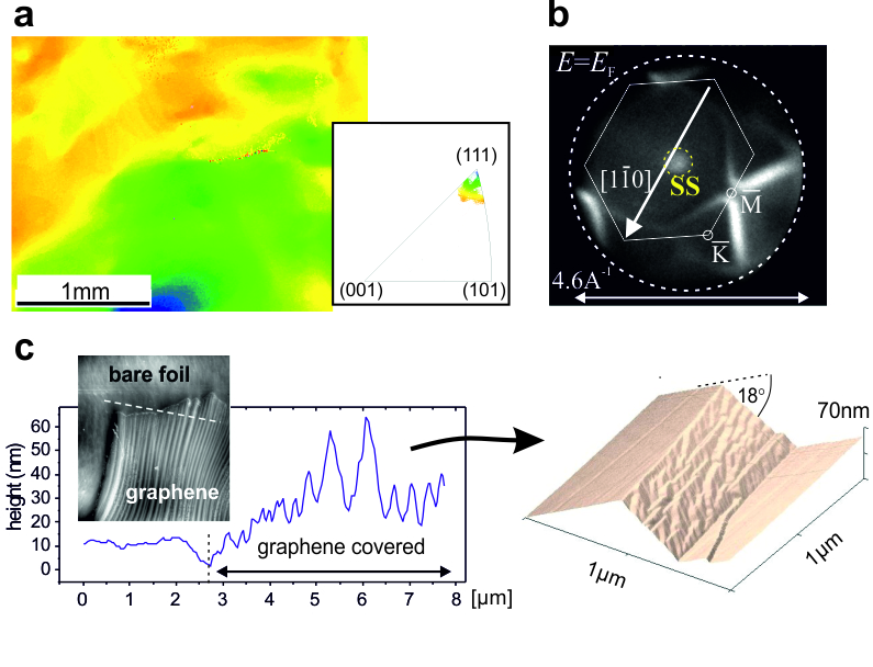
Electron backscattering diffraction (EBSD) in Fig. 1a reveals a Cu foil crystal orientation close to (111), however with local variations in the orientation defined by the color coding.
On the millimeter scale these variations correspond to angles smaller than , due to the waviness of the Cu foil. The inclination of the (111) direction with respect to the surface normal is directly visible in the -PEEM pattern in Fig. 1b, showing a high-index vicinal (111) cut of the copper‘s Fermi surface as developed after graphene removal by a mild Ar+ ion sputtering followed by C annealing in UHV.
The Fermi surface cut is tilted towards the labeled point according to the rotation vector [] indicated in the figure. Typical for photon excitation energies eV, the Mahan cone of the Cu(111) surface state (SS) is detected, which is shifted away from the center of the (111) orientation against the tilting direction Lobo and Mascaraque (2006); Baumberger et al. (2001).
Faceting process. Pulsed CVD leads to a characteristic graphene island morphology described in Fig. 1c. Atomic force microscopy (AFM) on larger graphene islands shows a characteristic stripe structure due to a pronounced roof-top shaped height modulation with varying canting angles of . Looking more closely, the roof-top structure is asymmetric and reveals a one sided complex faceted substructure on the nanometer scale. On the bare copper foil the roof-top modulation is absent, suggesting a graphene growth induced restructuring process, potentially related to the recently proposed feedback mechanism between the growing graphene and underlying mobile Cu atoms Wilson et al. (2013); Hayashi et al. (2013).
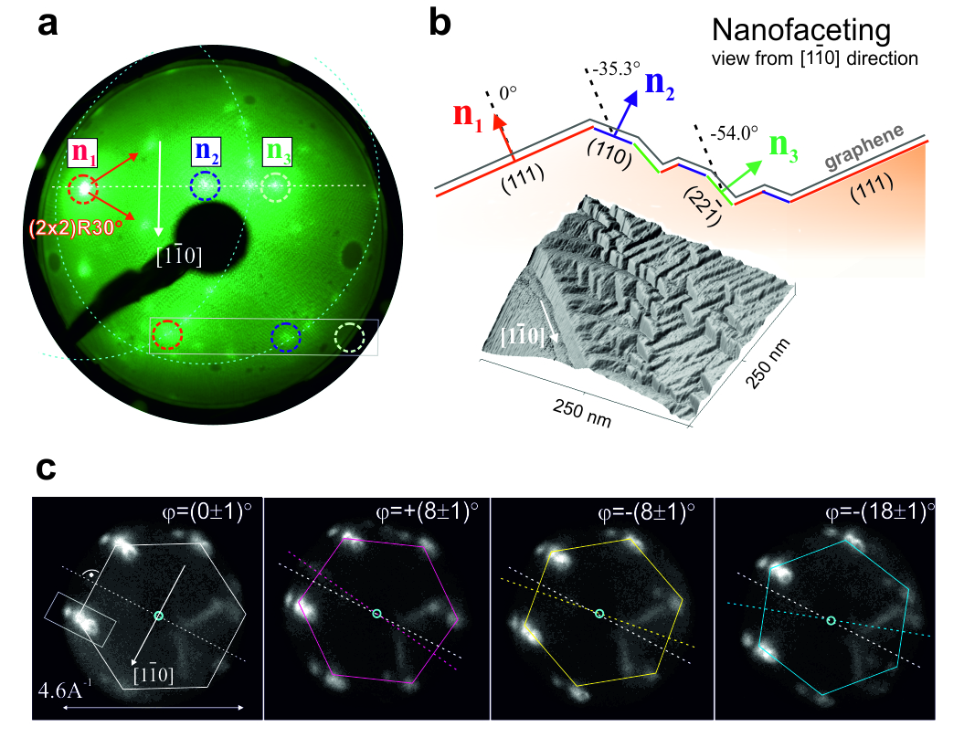
Reciprocal space methods LEED and -PEEM reveal further information on the graphene morphology and its domain orientations. Analysing energy-dependent LEED patterns shown in Supplementary Fig. S1, we can identify three specular spots. Specular spots correspond to elastically backscattered electron beams from local planes (zero order scattering of incoming beam), and thus for a uniformly flat surface one would expect only one. Here, they define three distinct facets with local surface normals , , and aligned perpendicular to the [] direction. has by far the largest intensity and thus dominates the surface area. Position-dependent LEED showed that the local surface normals are homogeneously oriented over millimeter scales on the copper foil. The diffraction LEED signal (first order scattering) in Fig. 2a, which averages over a mm spot on the sample, shows a few graphene rotational domains at once. Hexagonal LEED patterns of differently oriented coplanar graphene domains are expected to lay on a concentric circle around the supporting surface normal Walter et al. (2011); Hass et al. (2008). In our case, each of the three facets reproduce the same rotational domain hexagons on respective concentric circles, generating a characteristic triplet of replica spots (white box, showing one example domain spot on the three surface normals). For reasons of clarity in Fig. 2a we only indicate two of those circles corresponding to and .
The facets are resolved in detail by STM in Fig. 2b which unveils a length scale and shape reminiscent of CVD grown graphene on vicinal Ir(332) Šrut et al. (2013) or polycrystalline copper Rasool et al. (2011). Faceted surfaces typically self-assemble under the influence of monolayer coverages of adsorbates such as oxygen, sulfur, or metals as a result of anisotropies in the surface free energy [see e.g. Ref. Madey et al. (2008) for an overview]. In our case both carbon and oxygen seem to play a role, since local XPS on large graphene patches shows significant intensity of the O 1s core level peak (see Supplementary Fig. S2).
The influence of oxygen is directly evident for the dominant facet. In contrast to the other two facets it generates a distinct background LEED pattern, which corresponds to an oxygen p superlattice, rotated with respect to the Cu(111) reciprocal lattice (see red unit cell vectors in the LEED image),
recently reported by Gottardi et al. in 2015 Gottardi et al. (2015).
From the distance and alignment of the three specular spots on the LEED screen we can estimate the relative inclination angles of and with respect to Cu[111] with good accuracy. The rotation angles defined by the rotation vector [] amount to and , respectively. At a rotation angle of one expects the more open Cu(110) surface, which can be stabilized under the influence of adsorbates like oxygen or carbon ViolBarbosa et al. (2009). The rotation angle of the third facet’s normal with respect to (111) is consistent with that of a () orientation, which forms an angle of along the rotation direction []. It is the lowest index fcc facet in the respective angle range, and can explain the homogeneous and sharp specular spot observed in LEED.
Our model for the nanofaceted roof-top structure in Fig. 2b is further supported by -PEEM images in Fig. 2c performed with a 100m-wide spot. They confirm that although graphene rotations locally vary by significant relative angles, in this case , and , the replica spots remain oriented perpendicular to the [] direction as expected for a homogeneous facet-induced tilting of graphene hexagons in -space. In accordance with Ref. Rasool et al. (2011) it suggests that graphene crystal orientations grow continuously across different facets. The -PEEM pattern will be discussed in more detail below.
Symmetry of graphene growth.
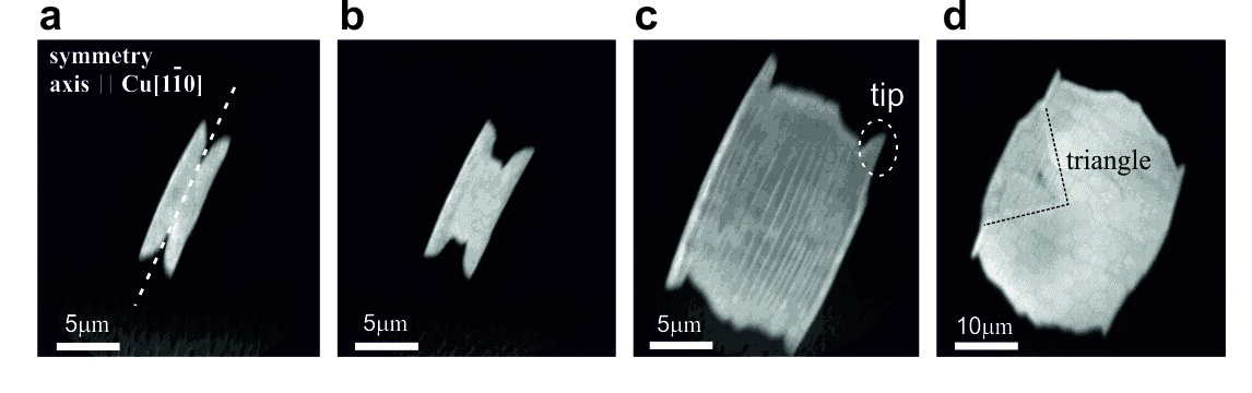
We are interested in understanding the local influence of the faceting process on graphene growth at the earliest stage. Fig. 3 shows typical small graphene islands, ranging from a few m to about 30m in width. They appear bright against the dark copper oxide background due to the work function contrast in the energy-filtered PEEM imaging mode. All islands obey a two-fold mirror symmetry, and their elongation along an axis oriented parallel to the Cu[] direction reflects the fundamental symmetry of the faceting direction. They exhibit a characteristic tip-shaped protuberance at the four extremities, and already host the characteristic roof-top modulation structure on the m scale.
Our island shapes strongly resemble those predicted recently by Meca et al. from phase-field models Meca et al. (2013), assuming markedly anisotropic carbon mobility on the metal surface. Anisotropic CVD growth usually reflects direction dependencies of e.g. chemical surface properties, or anisotropies in the morphology such as steps Zhang et al. (2012); Wofford et al. (2010); Hayashi et al. (2013); Tian et al. (2012). In our case this anisotropy is imprinted by the homogeneous vicinal Cu foil character with terraces predominantly separated by []-oriented step-edges, which renders the otherwise homogeneous carbon mass transport anisotropic during the CVD process. Under the influence of CVD the vicinal structure undergoes a surface-energy driven transition to the observed complex faceted structure including the m scale roof-top modulation. This process is facilitated by high temperatures close to the Cu melting temperature, and most likely counterbalanced by the built-up of elastic energy.
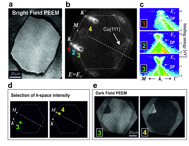
Doping Modulation. The self-organised faceting process during CVD is accompanied by a strong modulation of the electronic properties at the nanoscale. Fig. 4a shows another typical larger island of about 70m width. Using the spatially resolved -PEEM mode of our NanoESCA instrument, the ARPES signal of the particular graphene island is captured at the Fermi level , revealing the rather complex pattern shown in Fig. 4b. The dominant intensity depicts the characteristic hexagon of a oriented graphene domain indicated in white dashes, which exhibits the above discussed triplet replicas (denoted as 1, 2, and 3) according to the local facet planes , , and .
A second graphene domain (denoted as 4) with minor intensity appears at , again locked to the symmetry of the underlying Cu(111) intensity indicated by the arrow in Fig. 4b.
In Fig. 4c the dispersion relations of the three replicas at their respective K-points (1, 2, and 3) are shown as -space cuts in the direction . For flat 2D graphene -space information can be reduced to . The linear dispersion of valence and conduction bands touching at the so-called Dirac point (DP) is evident, typical of free-standing graphene with a dispersion , where is the Fermi velocity. At variance with free-standing graphene however, is not located at but shifted to higher binding energies, signifying
electron transfer towards the graphene system, so-called -doping, in accordance to previous results on graphene on homogeneous single crystalline Cu(001) and Cu(111) surfaces Walter et al. (2011). In our case substantially different doping levels coexist as a consequence of the three supporting facets with different interaction potentials. Starting from the hexagon
indicated as 1 with a -doping of eV, the energy position of the DP with respect to the Fermi level shifts to larger values eV and eV for replica K-points 2 and 3, respectively.
The differences in doping levels within the graphene island correspond to spatial modulations of the areal carrier densities, which due to the linear dispersion close to the DP are determined by the simple relation of the density of states , where is a function of the Fermi velocity (see supplementary). From the dispersion relations shown in Fig. 4c we fit the Fermi velocity to values of m/s, giving per (eV2 and graphene unit cell area) (see Supplementary Fig. S3). Integrating then allows to calculate the transferred carrier densities per area in units cm2 via the relation .
Doping levels at points 1, 2, and 3 thus correspond to carrier densities of 1.6, 3.3, and 5.7 cm-2, respectively. The large modulation by several cm-2 evidences the high efficiency of the nanofaceting process as a stamp for carrier modulations.
Dark-field characterisation. The findings raise the question if even more detailed assignments between real space and -space can be made. So far we showed ordinary bright-field PEEM images of graphene islands, where for each spot its entire -space signal contributes for imaging. The electron optics of our NanoESCA instrument, however, also allows for dark-field (DF) imaging Barrett et al. (2012), in which a certain -space intensity of interest is selected by a narrow aperture. Switching back to real space, the spatial origin of this -space signal can be to traced back in the respective PEEM image. Fig. 4d shows the aperture selection of the intensities at points 3 () and 4 () in -space, while the rest of -space intensity is blocked. In Fig. 4e the respective DF images are presented, resolving a highly symmetric triangular domain seed in a graphene host structure. Measurements on many different islands on our copper foils indeed confirm that triangular seeds are oriented along the same direction perpendicular to [] (see Supplementary Fig. S4). DF images at the three replica points 1, 2, and 3 show similar contrast as expected for large, m scale continuous graphene domains on a nanoscale faceted surface.
Discussion
The results of this study put forward a concept to achieve nanoscale doping modulations in chemical vapor deposited single layer graphene, exploiting surface energy driven faceting processes of supporting catalytic metals. For vicinal Cu(111) we show the self-assembly of coexisting copper (), (), and () nanofacets, which efficiently alternate graphene doping levels by several carriers per cm2 in a periodic manner. The concept is powerful since faceting geometry and associated directional modulation of doping levels is predefined by the vicinal orientation of the catalytic metal via the conservation of total substrate symmetry Chen and Richardson (2003). Indeed, for non-vicinal Cu(111) surfaces with sixfold rotational symmetry the faceting effect is absent, which leads to homogeneously doped graphene sheets only. A targeted manipulation of graphene based upon the choice of vicinal symmetry can thus be envisioned, using the knowledge on various surfactant-induced faceting phenomena on different surface materials at different temperatures Madey et al. (2008). Although in principle the equilibrium geometry of faceted surfaces are defined by the minimum of the total surface free energy, , where is the area and the area dependent specific surface free energy, precise predictions are often hampered by the fact that systems not always reach their thermodynamic equilibrium due to kinetic barriers in the faceting process. Nevertheless, due to the vast available parameter space in surface science our concept is potent and can be generalized to other chemical vapor deposited 2D systems in the focus of present research, such as semiconducting transition metal dichalcogenides, e.g. MoS2, insulating hexagonal boron nitride (h-BN) monolayers.
For graphene on vicinal Cu(111) studied in this work, we propose that the complex bottom-up faceting process is the result of anisotropic mobilities of carbon and copper atoms during high-temperature CVD close to the copper melting temperature. Mobilities and thus mass transport are asymmetric along and perpendicular to the vector [] characterising the vicinal surface orientation. This leads to strictly aligned graphene island nuclei with twofold rotational symmetry similar to those predicted recently by theory on CVD kinetics under anisotropic growth conditions Meca et al. (2013). Of vital importance for the understanding of the evident correlation between spatial and electronic band structure symmetries is the local wave-vector-resolved photoemission microscopy (-PEEM) technique, which enables to detect both real space and -space signals of a particular graphene island of a micrometer scale. Boundaries between rotational graphene domains resolved in the dark-field mode of -PEEM involve abrupt changes of the faceting morphology (see Supplementary Fig. S4, (b)-(d)), which underlines the intimate feedback between graphene and copper during the surface energy driven faceting processes.
Methods
Sample preparation
For the CVD growth of graphene islands we use m thick copper foils ( purity, Alpha
Aesar, reference 13382). A protective oxide is stripped by electrolysis in a copper sulfate solution before graphene grains are grown by CVD using the pulsed method as described in Ref. Han et al. (2014). 50 mm wide pieces of Cu foil are loaded into the CVD reactor then heated up to C under a sccm of argon at 3 mbar. Growth conditions are obtained by a series of 72 pulses of methane 4 sccm during sec separated by 50 sec long idling times. Argon and hydrogen input are kept constant during growth and respectively equal to 50 and sccm. The pressure is mbar during the full process.
Prior to surface sensitive UHV analysis techniques XPS, -PEEM, LEED, and STM the samples were annealed under UHV conditions for 30 min at temperatures of C to ensure cleanliness. If needed, graphene was removed by mild Ar+-ion sputtering at room temperature (mbar argon pressure, cathode voltage 1 kV, 40 min) followed by C annealing under UHV.
Measurement techniques
XPS and -PEEM measurements were done using an Omicron NanoESCA instrument with laboratory light sources. The photoemission spectrometer is based on a PEEM column and a imaging double hemispherical energy filter Krömker et al. (2008). A transfer lens in the electron optics switches between real space and angular resolved -PEEM mode, which allows to detect classical x-ray photoemission spectra with monochromatized Al radiation, as well as an energy dependent mapping of the Brillouin zone using a helium discharge lamp at eV with a resolution of
eV. In the -PEEM mode the Fermi edge is derived from the kinetic energy at which the k-PEEM intensity is cut off. We define this energy as zero binding energy and expect the error of this Fermi level estimation to be eV.
For dark field measurements, apertures sizes m were positioned to select intensities of interest in -space. Thereafter, dark field PEEM images were taken in the respective telescopic mode. In order to minimize parasitic signals, the iris aperture was narrowed down to encompass the graphene island of choice. See also Ref. Barrett et al. (2012) for further details.
Electron backscatter diffraction (EBSD) data was aquired with an EDAX camera and software on a Tescan FERA 3 instrument. Detailed technical information can be found in Ref. Wright et al. (2015). For atomic force microscopy (AFM) a Bruker Dimension Icon was employed. Both EBSD and AFM were performed under ambient conditions.
Scanning tunneling microscopy (STM) was done at room temperature under UHV conditions (mbar) using an Omicron VT-STM.
Acknowledgements
We thank Konrad Winkler from Omicron for helpful discussions. The authors acknowledge financial support from the Ministry of Education, Youth and Sport of the Czech Republic (Research infrastructures
SAFMAT LM2011029 and LO1409), and the EU Graphene Flagship. JH acknowledges the Purkyně Fellowship program of the Academy of Sciences of the Czech Republic.
Author Contributions
D. K. prepared the samples. M. V. measured -PEEM and dark field PEEM. L. F. and M. K. provided scanning force and tunneling microscopy images, respectively. J. K. contributed with EBSD data. J. H. prepared the main manuscript text and figures together with J. C.. J. L. and V. B. reviewed the manuscript.
Additional Information
Competing financial interests: The authors declare no competing financial interests.
References
- (1)
- Yazyev and Louie (2010) O. V. Yazyev and S. G. Louie, Nature Materials 9, 806 (2010).
- Van Tuan et al. (2013) D. Van Tuan et al., Nano Letters 13, 1730 (2013).
- Ĉervenka et al. (2009) J. Červenka, M. I. Katsnelson, and C. F. J. Flipse, Nature Physics 5, 840 (2009).
- Chiu et al. (2010) H.-Y. Chiu, V. Perebeinos, Y.-M. Lin, and P. Avouris, Nano Letters 10, 4634 (2010).
- Williams et al. (2007) J. R. Williams, L. DiCarlo, and C. M. Marcus, Science 317, 638 (2007) .
- Allain and Fuchs (2011) P. Allain and J. Fuchs, The European Physical Journal B 83, 301 (2011).
- Castro-Neto and ? (2009) A. H. Castro-Neto F. Guinea, N. M. R. Peres, K. S. Novoselov, and A. K. Gaim, Review of Modern Physics 81, 109 (2009).
- Cheianov et al. (2007) V. V. Cheianov, V. Fal’ko, and B. L. Altshuler, Science 315, 1252 (2007).
- Cayssol et al. (2009) J. Cayssol, B. Huard, and D. Goldhaber-Gordon, Phys. Rev. B 79, 075428 (2009).
- Park et al. (2008) C.-H. Park, L. Yang, Y.-W. Son, M. L. Cohen, and S. G. Louie, Nature Physics 4, 213 (2008).
- Young and Kim (2009) A. F. Young and P. Kim, Nature Physics 5, 222 (2009).
- Katsnelson et al. (2006) M. I. Katsnelson, K. S. Novoselov, and A. K. Geim, Nature Physics 2, 620 (2006).
- Walter et al. (2011) A. L. Walter et al., Phys. Rev. B 84, 195443 (2011).
- Pinshane (2011) Y. H. Pinshane, Nature 469, 389 (2011).
- Starodub et al. (2011) E. Starodub et al., Phys. Rev. B 83, 125428 (2011).
- Avila et al. (2013) J. Avila et al., Science Reports 3, 1252 (2013).
- Han et al. (2014) Z. Han et al., Advanced Functional Materials 24, 964 (2014).
- Lobo and Mascaraque (2006) J. Lobo and A. Mascaraque, Journal of Physics: Condensed Matter 18, L395 (2006).
- Baumberger et al. (2001) F. Baumberger, T. Greber, and J. Osterwalder, Phys. Rev. B 64, 195411 (2001).
- Wilson et al. (2013) N. R. Wilson et al., Nano Research 6, 99 (2013).
- Hayashi et al. (2013) K. Hayashi, S. Sato, and N. Yokoyama, Nanotechnology 24, 025603 (2013).
- Hass et al. (2008) J. Hass et al., Phys. Rev. Lett. 100, 125504 (2008).
- Šrut et al. (2013) I. Šrut, V. M. Trontl, P. Pervan, and M. Kralj, Carbon 56, 193 (2013).
- Rasool et al. (2011) H. I. Rasool et al., Nano Letters 11, 251 (2011), pMID: 21117698.
- Madey et al. (2008) T. E. Madey, W. Chen, H. Wang, P. Kaghazchi, and T. Jacob, Chem. Soc. Rev. 37, 2310 (2008).
- Gottardi et al. (2015) S. Gottardi et al., Nano Letters 15, 917 (2015).
- ViolBarbosa et al. (2009) C. E. ViolBarbosa, J. Fujii, G. Panaccione, and G. Rossi, New Journal of Physics 11, 113046 (2009).
- Meca et al. (2013) E. Meca, J. Lowengrub, H. Kim, C. Mattevi, and V. B. Shenoy, Nano Letters 13, 5692 (2013).
- Zhang et al. (2012) B. Zhang et al., ACS Nano 6, 2471 (2012).
- Wofford et al. (2010) J. M. Wofford, S. Nie, K. F. McCarty, N. C. Bartelt, and O. D. Dubon, Nano Letters 10, 4890 (2010), pMID: 20979362.
- Tian et al. (2012) J. Tian et al., Nano Letters 12, 3893 (2012).
- Barrett et al. (2012) N. Barrett, E. Conrad, K. Winkler, and B. Krömker, Review of Scientific Instruments 83, 083706 (2012).
- Krömker et al. (2008) B. Krömker et al., Review of Scientific Instruments 79, 053702 (2008).
- Wright et al. (2015) S. I. Wright, M. M. Nowell, R. de Kloe, P. Camus, and T. Rampton, Ultramicroscopy 148, 132 (2015).
- Chen and Richardson (2003) Q. Chen and N. V. Richardson, Progress in Surface Science 73, 59 (2003).