Design Rules for High Performance Tunnel Transistors from 2D Materials
I Abstract
Tunneling field-effect transistors (TFETs) based on 2D materials are promising steep sub-threshold swing (SS) devices due to their tight gate control. There are two major methods to create the tunnel junction in these 2D TFETs: electrical and chemical doping. In this work, design guidelines for both electrically and chemically doped 2D TFETs are provided using full band atomistic quantum transport simulations in conjunction with analytic modeling. Moreover, several 2D TFETs’ performance boosters such as strain, source doping, and equivalent oxide thickness (EOT) are studied. Later on, these performance boosters are analyzed within a novel figure-of-merit plot (i.e. constant ON-current plot).
II Introduction
Transistor scaling has driven device designs toward thinner channels for better gate control over the channel. 2D materials can provide a shortcut to the ultimate channel thickness scaling: an atomically thin channel. A tight gate control is important in FETs to obtain a 1-to-1 band movement in the channel potential with respect to the gate voltage. The tight gate control is even more crucial for the performance of tunnel FETs (TFETs) [1, 2] since the scaling length and accordingly tunneling distance decreases with a better gate control [3, 4, 6, 5, 7, 8, 9, 10]. The exponential dependence of the tunneling current on the tunneling distance emphasizes the role of a thin channel and tight gate control in TFETs.
Some 2D materials, such as graphene or silicene suffer from the lack of a bandgap () and are not suitable for transistor applications. On the other hand, 2D materials such as transition metal dichacogenides (TMD: MoS2, WSe2, MoTe2, etc.) exhibit a sizable direct bandgap in their monolayer configuration. Among those, monolayer WTe2 shows particular promise for high performance TFET applications [4] due to its rather small effective mass and an expected bandgap of about 0.75eV [13]. Note that a bandgap of about provides the best performance in TFETs, where is the supply voltage [11], which means that for a of about 0.5V an range of 0.55-0.75eV is expected to provide best performance. Unfortunately, however, experiments indicate that the WTe2 2H phase may not be stable [14].
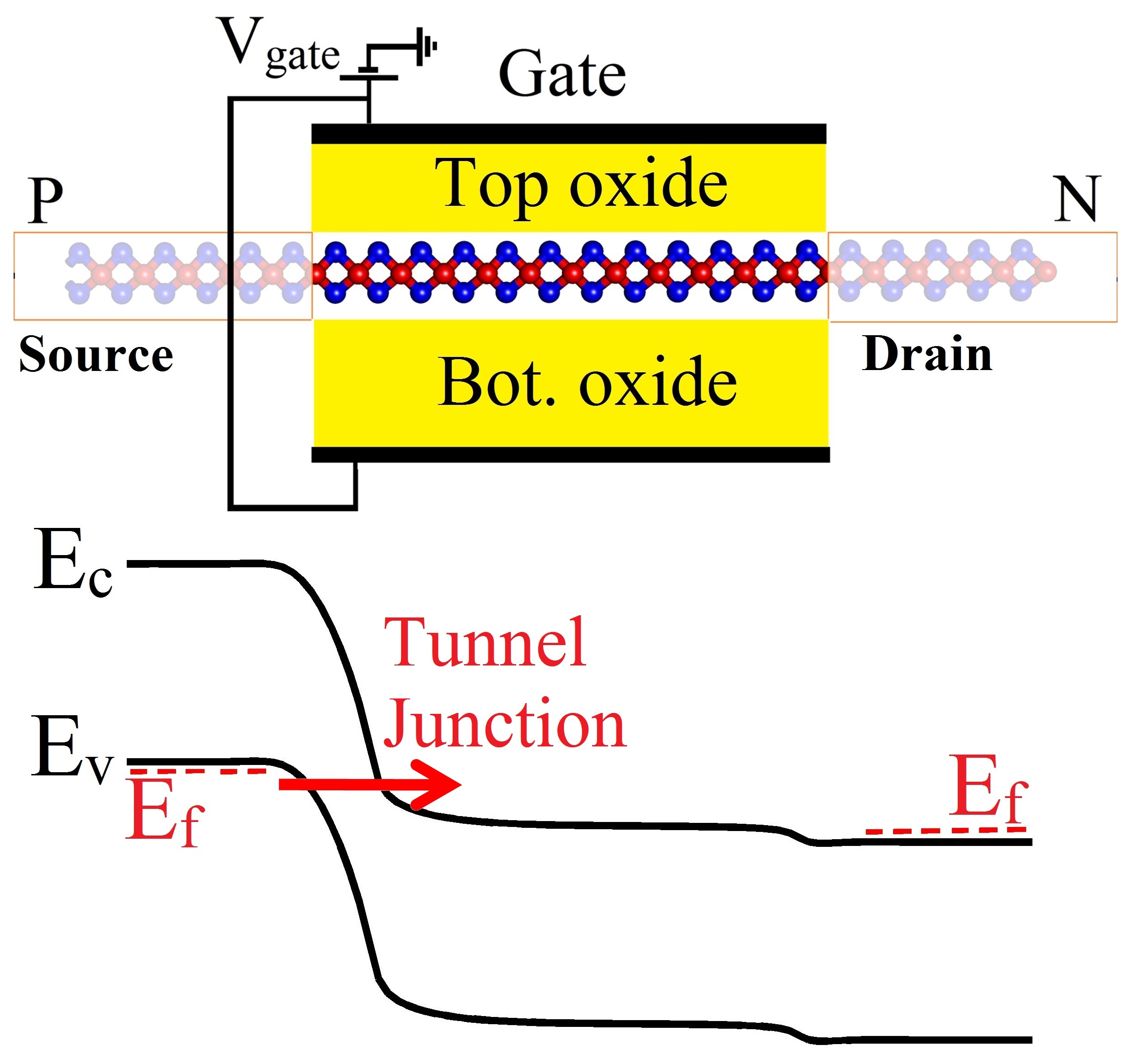
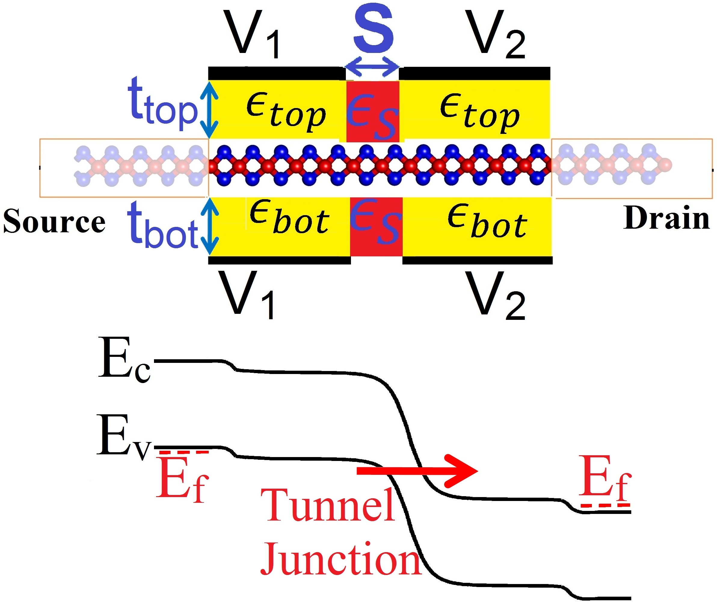
This makes it essential to look for other methods for improving the performance of TMD TFETs utilizing the existing set of semiconducting TMDs. There are two major methods to create the tunnel junction in these 2D TFETs: electrical [18, 19] and chemical doping [15]. The device structure of a chemically doped (CD) and electrically doped (ED) TFET are shown in Fig. 1. In the case of CD-TFETs (Fig. 1a), the tunnel junction is created between a doped source region and the electrostatically gated region. High doping of the source region fixes the potential at the source side. Increasing the gate voltage can reduce the potential in the channel and create in this way a p-n like tunnel junction. In the case of ED-TFETs (Fig. 1b), n- and p-type potentials are defined by two gates at the two sides of the tunnel junction and no chemical dopants exist close to the tunnel junction. Avoiding chemical doping in the tunnel region has several advantages. In particular, it avoids: 1) dopant fluctuations and threshold voltage shifts [23], 2) dopant states within the bandgap which reduce the OFF-state performance [20, 21], and 3) the challenging task of chemically doping 2D materials [22].
In this work, different performance boosters for chemically and electrically doped 2D TFETs are discussed in detail. First, atomistic quantum transport simulations from NEMO5 tool [33, 34, 35] have been used to investigate the impact of strain, source doping level, and equivalent oxide thickness (EOT). Later on, an analytic model is used to explain the trends.
III Simulation method
According to our previous analysis [4] WSe2 is the next best choice in terms of existing TMD materials for TFET applications after WTe2. Hence, monolayer WSe2 is chosen for our atomistic simulations and the detailed analysis of various performance boosters. The WSe2 Hamiltonian employs an sp3d5 2nd nearest neighbor tight-binding (TB) model. The semi-empirical TB parameters are optimized based on first principles bandstructures (E-K) calculated from density functional theory (DFT) with the generalized gradient approximation (GGA) [4]. A similar TB parameter fitting procedure based on DFT E-K has been used in the presence of strain. DFT-GGA has been chosen since it provides band gaps and effective masses in TMDs comparable to experimental measurements [13].
In this work, self-consistent Poisson-NEGF (non-equilibrium Green’s function) methodology has been employed within the tight-binding description. Because in-plane and out-of-plane dielectric constants ( and ) of WSe2 are different, the Poisson equation reads as follows [4] if the z direction is considered to be along the c-axis of the TMDs:
| (1) |
where and are the electrostatic potential and total charge, respectively. The dielectric constant values ( and ) of WSe2 are taken from ab-initio studies [24]. In this work, quantum transport simulations have been performed with our simulation tool NEMO5 [33, 34, 35].
IV Results
In spite of the similarities between CD-TFETs and ED-TFETs, they obey rather different scaling rules and design guidelines [26, 29]. We will discuss the impact of the various performance boosters in CD-TFETs and ED-TFETs in the following sections.
IV-A Chemically doped TMD TFETs
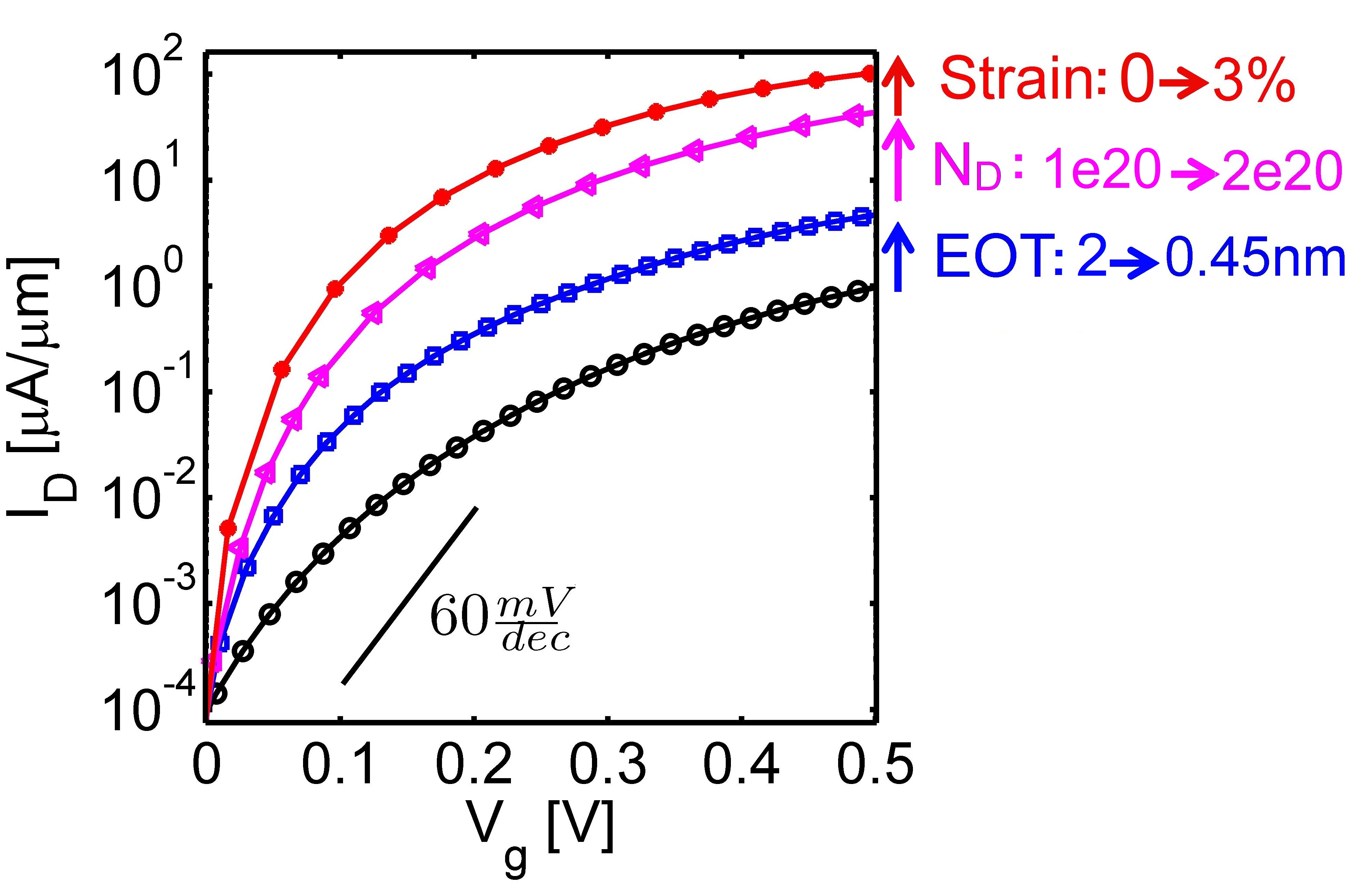
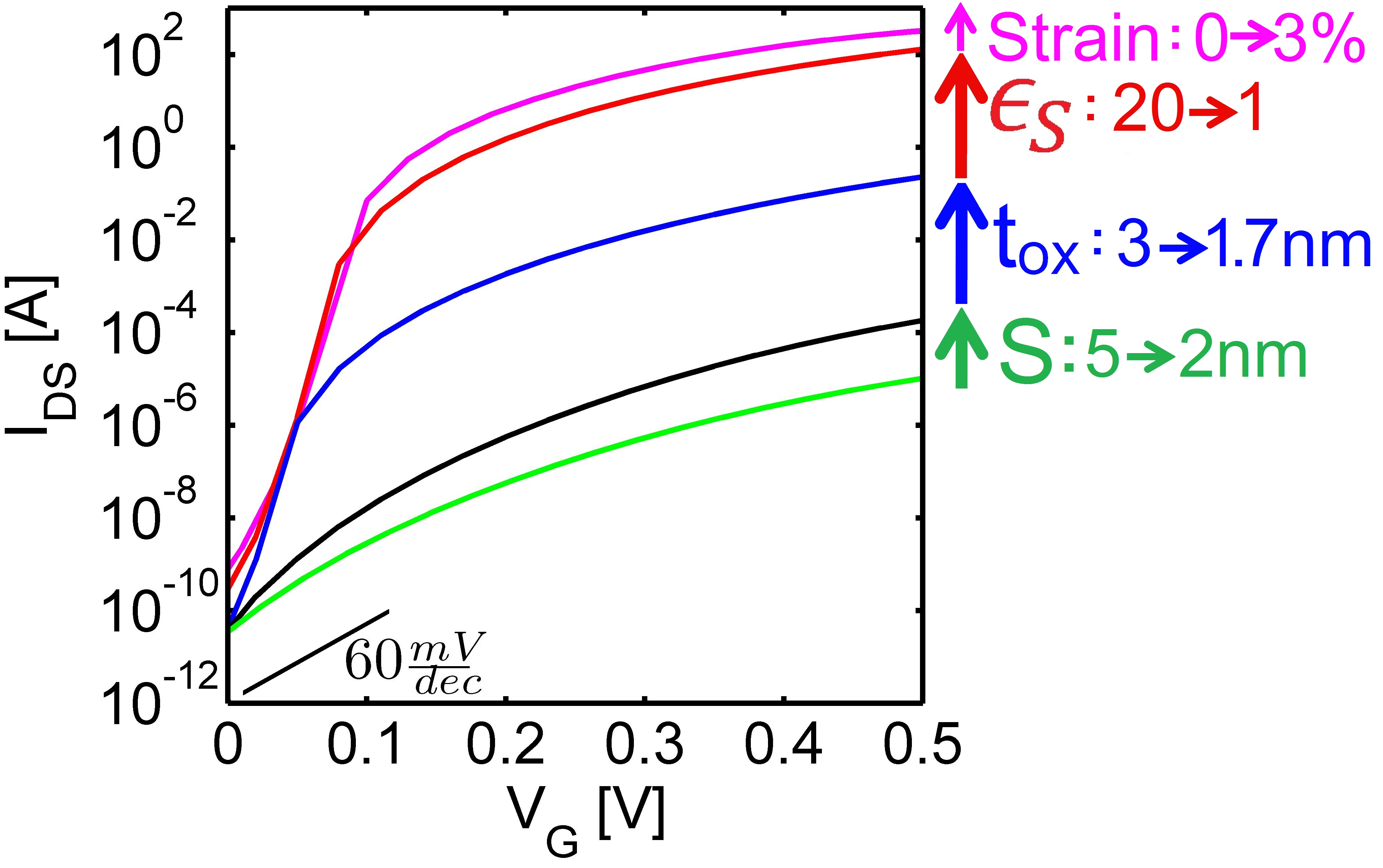
First, the design aspects of chemically doped (CD) TFETs are studied with the structure shown in Fig. 1a. A 15nm long monolayer WSe2 channel with VDD of 0.5V is considered in all CD-TFET simulations. We have identified a number of critical factors enhancing the performance of 2D CD-TFETs: strain, high doping levels of the source (), and small EOT values. Fig. 2 shows transfer characteristics of a WSe2 CD-TFET. The black current-voltage (I-V) curve shows the results for the reference transistor with an EOT=2nm, =1e20 cm-3, and no strain. At the first step, EOT is decreased to 0.45nm (blue curve). In the second step, the doping level is increased to 2e20 cm-3 (pink curve), and finally a biaxial strain of 3% is applied to WSe2 (red curve). The bandgap and effective mass of monolayer WSe2 decreases by application of biaxial strain; e.g. 3% biaxial strain reduces the reduced effective mass and the band gap by about 10% and 22%, respectively. Application of all performance boosters increases ION by more than 2 orders of magnitude.
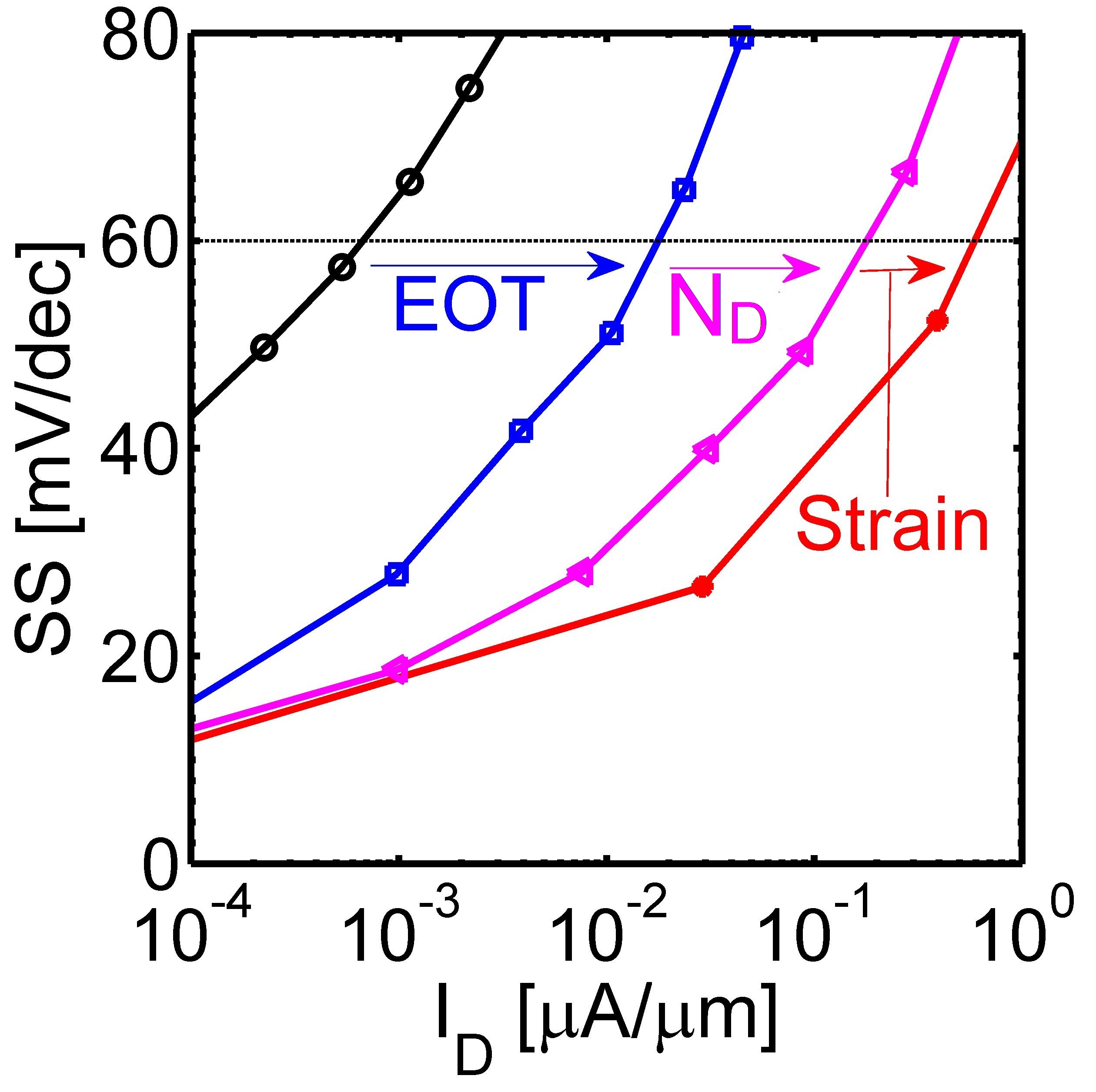
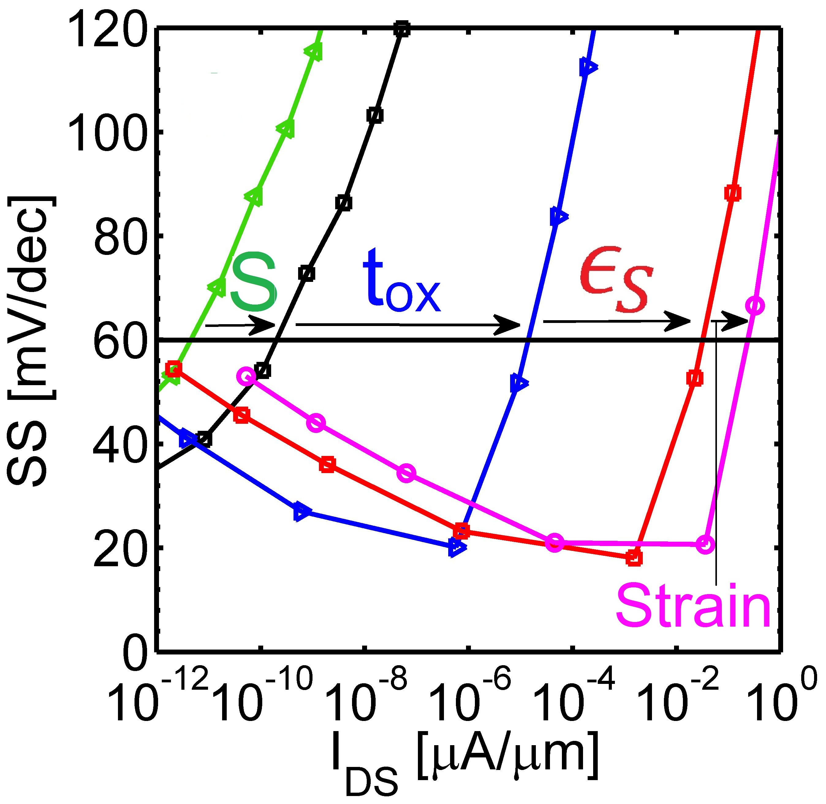
Fig. 3 shows the impact of the performance boosters (i.e. strain, source doping, and EOT) on the OFF-state performance. SS is plotted versus the drain current at which SS is calculated [28]. It is shown that the performance boosters not only increase ION, but also increase I60 (the current level where SS=60 mV/dec [36]) and decrease SS. About 3 orders of magnitude increase in I60 and a factor of 3 reduction in SS are obtained combining the performance boosters.
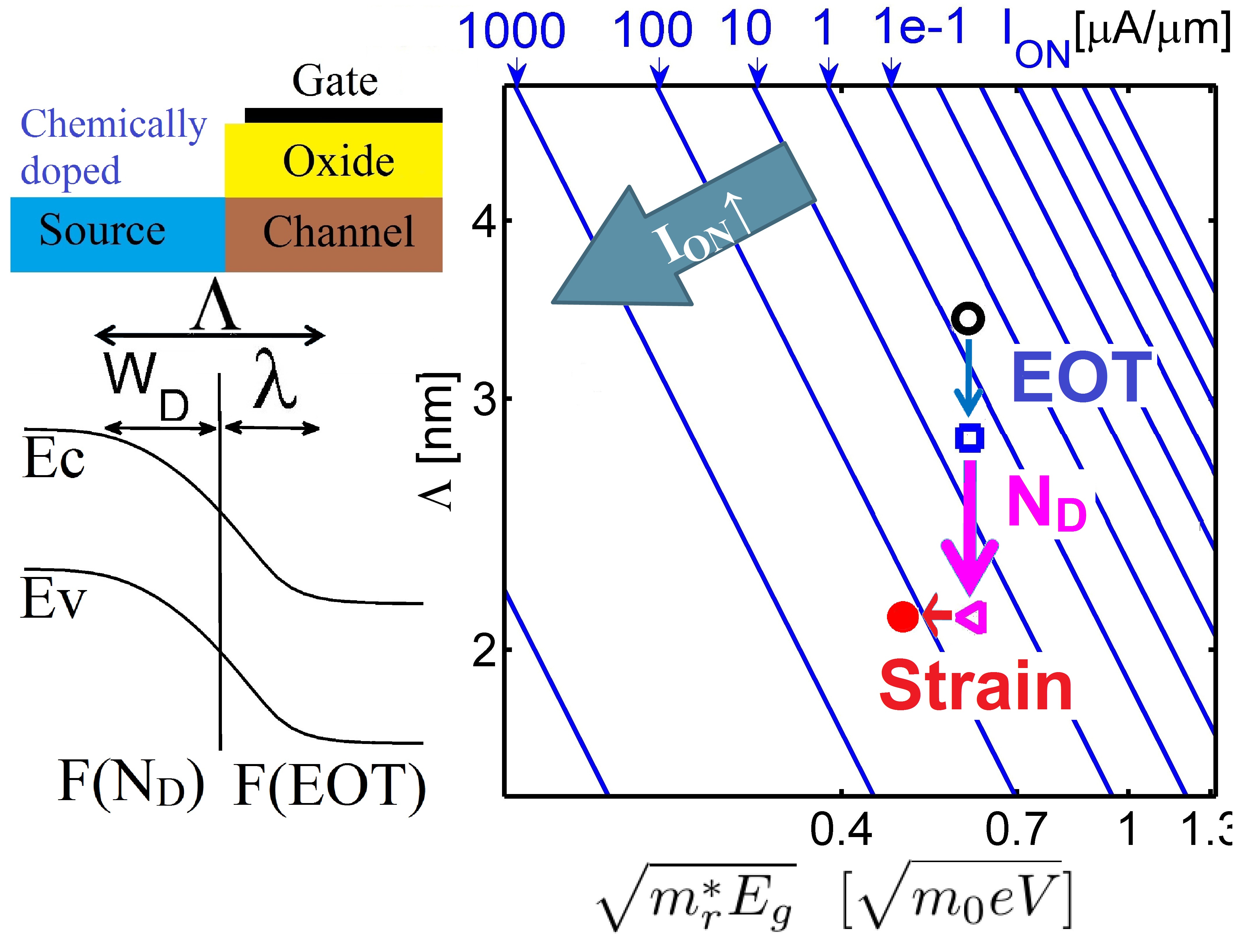
The ON-state performance of TFETs mainly depends on 1) the band bending distance (shown in Fig. 4) which is determined by the device design and 2) the channel material properties: and [26]. Fig. 4 shows a constant ON-current plot. Notice that ION depends exponentially on the product of and and since both axes are plotted on a logarithmic scale, constant current contours appear as parallel lines [27]. To achieve a higher ION, one can reduce or . In CD-TFETs, is composed of two terms: 1) the scaling length () under the gated region and 2) the source depletion width (WD). Increasing the source doping level, reduces WD, and reducing the EOT, reduces . Consequently is also reduced. On the other hand, strain changes the material properties without affecting . Fig. 4 therefore portrays the interplay between design and material parameters and the impact of the various performance boosters.
IV-B Electrically doped TMD TFETs
In this part, the performance analysis of 2D electrically doped (ED) TFETs is discussed. Notice that the design guidelines for ED-TFETs are rather different due to the presence of fringing fields. Fig. 1b shows the schematic of a double gated ED-TFET [29]. In ED-TFETs, the tunnel junction is created through two adjacent gates with opposite polarities. One of these 2 gates is a conventional gate and the other one is connected to the source contact which tunes the electrically induced doping level of that side. Each gate has a length of 12nm and VDS is set to 0.5V in all ED-TFET simulations. The major players affecting the performance of ED-TFETs are: 1) the spacing between the gates: (Fig. 1b), 2) the thickness of the oxide (not the EOT), 3) the dielectric constant of the spacing region () [32], and 4) strain. Fig. 5 shows that and have much higher impact on the performance of ED-TFETs compared to and strain.
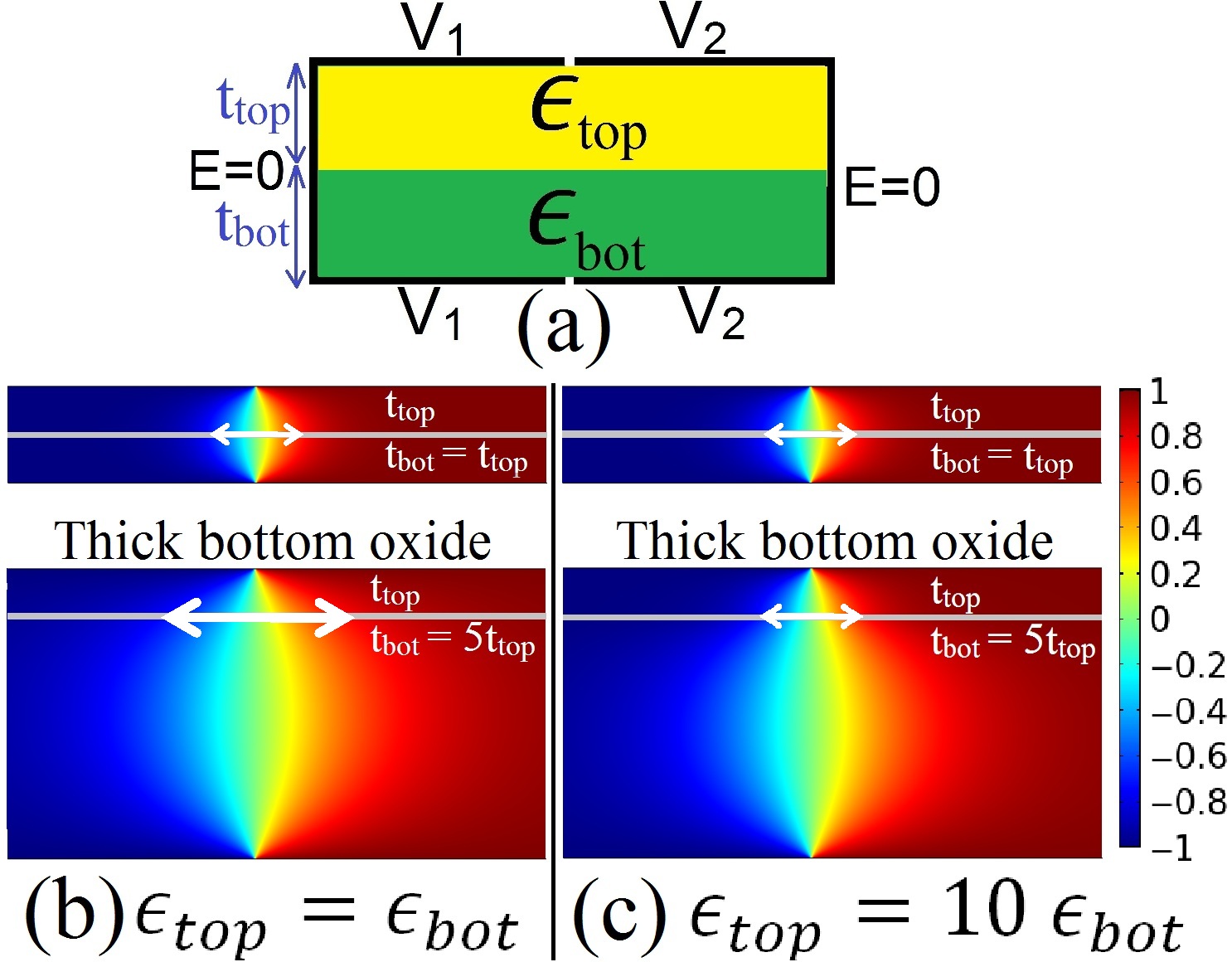

Fig. 6 shows how the OFF-state performance of the 2D ED-TFETs gets affected by different design parameters. It is apparent that both SS and I60 significantly improve using a thinner oxide, smaller spacing, and a smaller spacer dielectric constant. The most effective improvement comes from a smaller spacer dielectric constant and thinner oxide which increases I60 by more than 4 orders of magnitude.
One of the main differences between 2D CD-TFETs and ED-TFETs is that the concept of EOT is not applicable to ED-TFETs. In the case of ED-TFETs, the electric field at the tunnel junction () is inversely proportional to the total thickness of the device (including top and bottom oxides) [29, 30, 31]:
| (2) |
This point is usually ignored in the design of electrically doped devices; a common layout uses a thick back oxide which leads to a small . This problem can be overcome by using a back oxide with low dielectric constant compared to the top oxide (). Fig. 7b shows the potential profile of an electrically doped TFETs with thin and thick back oxides with high-k dielectric on the top and bottom. It is apparent that a thick back oxide increases the potential spread and reduces . Fig. 7c shows that a low-k dielectric back gate can reduce the impact of thick back gate oxide significantly. Hence,
| (3) |
These results suggests that if a thin back oxide with gates aligned with the top gates is experimentally challenging, one can use a low-k back oxide to avoid performance degradation and enhance fabrication feasibility.
Conclusion
In conclusion, important design parameters of 2D CD- and ED-TFETs are discussed here. It is shown that the EOT and source doping () are the main players in the case of CD-TFETs, whereas the performance of ED-TFETs mainly depends on and . Considering performance boosters can in principle increase the ON-current of both CD- and ED-TFETs by orders of magnitude.
References
- [1] J. Appenzeller, Y.-M. Lin, J. Knoch, and Ph. Avouris, ”Band-to-band tunneling in carbon nanotube field-effect transistors,” Phys. Rev. Lett., vol. 93, no. 19, pp. 196805 (2004).
- [2] J. Appenzeller, Y.-M. Lin, J. Knoch, and Ph. Avouris, Comparing carbon nanotube transistors - The ideal choice: A novel tunneling device design, IEEE Trans. on Elec. Dev. 52, 2568-2576 (2005).
- [3] D. Sarkar et al., ”A subthermionic tunnel field-effect transistor with an atomically thin channel,” Nature, 526(7571), 91-95 (2015).
- [4] H. Ilatikhameneh, Y. Tan, B. Novakovic, G. Klimeck, R. Rahman, J. Appenzeller, ”Tunnel Field-Effect Transistors in 2D Transition Metal Dichalcogenide Materials,” IEEE Exploratory Solid-State Computational Devices and Circuits, vol. 1, no. 1, pp. 12-18 (2015), DOI: 10.1109/JXCDC.2015.2423096.
- [5] S. Das, A. Prakash, R. Salazar, and J. Appenzeller, Towards low power electronics: Tunneling phenomena in TMDs, ACS Nano 8, 2, 1681–1689 (2014).
- [6] G. Fiori, F. Bonaccorso, G. Iannaccone, T. Palacios, D. Neumaier, A. Seabaugh, S. K. Banerjee, and L. Colombo, ”Electronics based on two-dimensional materials,” Nature Nanotechnology vol. 9, no. 10, pp. 768-779, (2014).
- [7] A. Seabaugh, S. Fathipour, W. Li et al., ”Steep subthreshold swing tunnel FETs: GaN/InN/GaN and transition metal dichalcogenide channels,” In 2015 IEEE International Electron Devices Meeting (IEDM, pp. 35-6, (2015, December)
- [8] P. Zhao, S. Desai, M. Tosun, T. Roy, H. Fang, A. Sachid et al., ”2D Layered Materials: From Materials Properties to Device Applications,” IEDM (2015).
- [9] F. Liu et al. ”A Theoretical Investigation of Orientation-Dependent Transport in Monolayer MoS2 Transistors at the Ballistic Limit,” Electron Device Letters, IEEE 36.10 (2015): 1091-1093.
- [10] T.A. Ameen, H. Ilatikhameneh, G. Klimeck, and R. Rahman ”Few-layer Phosphorene: An Ideal 2D Material For Tunnel Transistors,” [Online.] arXiv:1512.05021 (2015).
- [11] H. Ilatikhameneh et al., ”Can Homojunction Tunnel FETs Scale Below 10nm?” IEEE EDL, vol. 37, no. 1, pp. 115-118 (2016).
- [12] D. J. Frank, and H. S. P. Wong, ”Analysis of the design space available for high-kgate dielectrics in nanoscale MOSFETs,” Superlattices and Microstructures, vol. 28, no. 5, pp. 485-491, (2000).
- [13] C. Gong, H. Zhang, W. Wang, L. Colombo, R. M. Wallace, and K. Cho, Band alignment of two-dimensional transition metal dichalcogenides: application in tunnel field effect transistors, Appl. Phys. Lett. 103, 053513 (2013).
- [14] C. H. Lee, E. C. Silva, L. Calderin, M. A. T. Nguyen, M. J. Hollander, B. Bersch et al. ”Tungsten Ditelluride: a layered semimetal,” Scientific reports, 5 (2015).
- [15] L. Yang et al., Chloride Molecular Doping Technique on 2D Materials: WS2 and MoS2, Nano letters 14.11, 6275-6280 (2014).
- [16] B. Radisavljevic, A. Radenovic, J. Brivio, V. Giacometti and A. Kis, ”Single-layer MoS2 transistors,” Nature Nano., vol. 6, pp. 147–150 (2011).
- [17] M. Salmani-Jelodar, S. Mehrotra, H. Ilatikhameneh, and G. Klimeck, ”Design Guidelines for Sub-12 nm Nanowire MOSFETs,” IEEE Trans. on Nanotechnology, vol. 14, no. 2, pp. 210-213 (2015).
- [18] J. R. Williams, L. DiCarlo, and C. M. Marcus, ”Quantum Hall effect in a gate-controlled pn junction of graphene,” Science, vol. 317, pp. 638-641 (2007).
- [19] J. F. Tian, L. A. Jauregui, G. Lopez, H. Cao, and Y. P. Chen, ”Ambipolar graphene field effect transistors by local metal side gates,” Applied Physics Letters, vol. 96, no. 26, pp. 263110 (2010).
- [20] S. Agarwal, and E. Yablonovitch, ”Band-Edge Steepness Obtained From Esaki/Backward Diode Current–Voltage Characteristics,” IEEE Transaction on Electron Devices, vol. 61, no. 5, pp. 1488-1493 (2014).
- [21] M. G. Pala et al., IEEE Trans. on Electron Devices 60, no. 9, 2795-2801 (2013).
- [22] J. C. Ho et al. ”Controlled nanoscale doping of semiconductors via molecular monolayers.” Nature materials 7.1, pp. 62-67 (2008).
- [23] F. W. Chen, H. Ilatikhameneh, G. Klimeck, Z. Chen, and R. Rahman, ”Configurable Electrostatically Doped High Performance Bilayer Graphene Tunnel FET,” [Online.] arXiv:1509.03593 (2015).
- [24] A. Kumar and P. K. Ahluwali, Tunable dielectric response of transition metals dichalcogenides MX2 (M=Mo, W; X=S, Se, Te): Effect of quantum confinement, Physica B 407, 4627–4634 (2012).
- [25] R.-H. Yan et al., ”Scaling the Si MOSFET: from bulk to SOI to bulk,” IEEE Trans. Electron Devices, vol. 39, no. 7, pp. 1704-1710 (1992).
- [26] R. B. Salazar, H. Ilatikhameneh, R. Rahman, G. Klimeck, J. Appenzeller, ”A predictive analytic model for high-performance tunneling field-effect transistors approaching non-equilibrium Green’s function simulations,” Journal of Applied Physics, 118, 164305 (2015), DOI:http://dx.doi.org/10.1063/1.4934682
- [27] H. Ilatikhameneh, R. B. Salazar, G. Klimeck, R. Rahman, J. Appenzeller, ”From Fowler-Nordheim to Non-Equilibrium Green’s Function Modeling of Tunneling.” [Online] arXiv:1509.08170 (2015).
- [28] H. Lu, and A. Seabaugh, ”Tunnel field-effect transistors: state-of-the-art,” Electron Devices Society, IEEE Journal of the, 2(4), pp.44-49 (2014).
- [29] H. Ilatikhameneh, G. Klimeck, J. Appenzeller, R. Rahman, ”Scaling Theory of Electrically Doped 2D Transistors,” IEEE Electron Device Letters, DOI: 10.1109/LED.2015.2436356 (2015).
- [30] H. Ilatikhameneh, R. Rahman, J. Appenzeller, and G. Klimeck, ”Electrically doped WTe 2 tunnel transistors,” IEEE, International Conference on Simulation of Semiconductor Processes and Devices (SISPAD, pp. 270-272 (2015).
- [31] H. Ilatikhameneh et al. ”Electrically doped 2D material tunnel transistor,” IEEE, International Workshop on Computational Electronics (IWCE) (2015).
- [32] H. Ilatikhameneh, T. Ameen, G. Klimeck, J. Appenzeller, and R. Rahman, ”Dielectric Engineered Tunnel Field-Effect Transistor,” IEEE Electron Device Letters (2015), 10.1109/LED.2015.2474147.
- [33] J. E. Fonseca, T. Kubis, M. Povolotskyi, B. Novakovic, A. Ajoy, G. Hegde, H. Ilatikhameneh, Z. Jiang, P. Sengupta, Y. Tan, G. Klimeck, ”Efficient and realistic device modeling from atomic detail to the nanoscale,” Journal of Computational Electronics, vol. 12, no. 4, pp. 592-600 (2013).
- [34] S. Steiger, M. Povolotskyi, H. H. Park, T. Kubis, and G. Klimeck, ”NEMO5: a parallel multiscale nanoelectronics modeling tool,” IEEE Transaction on Nanotechnology, vol. 10, no. 6, pp. 1464-1474 (2011).
- [35] J. Sellier, et al., ”Nemo5, a parallel, multiscale, multiphysics nanoelectronics modeling tool,” SISPAD, (2012).
- [36] W. G. Vandenberghe, A. S. Verhulst, B. Sor ̵́ee, W. Magnus, G. Groeseneken, Q. M. Heyns, and M. V. Fischetti, ”Figure of merit for and identification of sub-60 mv/decade devices,” Applied Physics Letters, vol. 102, no. 1, p. 013510, (2013).