Disentangling nonradiative recombination processes in Ge micro-crystals on Si substrates
Abstract
We address nonradiative recombination pathways by leveraging surface passivation and dislocation management in m-scale arrays of Ge crystals grown on deeply patterned Si substrates. The time decay photoluminescence (PL) at cryogenic temperatures discloses carrier lifetimes approaching 45 ns in band-gap engineered Ge micro-crystals. This investigation provides compelling information about the competitive interplay between the radiative band-edge transitions and the trapping of carriers by dislocations and free surfaces. Furthermore, an in-depth analysis of the temperature dependence of the PL, combined with capacitance data and finite difference time domain modeling, demonstrates the effectiveness of in passivating the surface of Ge and thus in enhancing the room temperature PL emission.
The monolithic development of Si photonic components addresses the hurdles of charged-based computing and is expected to drastically transform information and communication technologies. The progress of Si photonics, however, has been jeopardized by fundamental limitations. The centrosymmetric crystal structure and the indirect nature of the band-gap of bulk Si imply weak electro-optical effects alongside poor absorption and emission efficiencies.Leuthold et al. (2010) These obstacles have stimulated the exploration of wafer-scale fabrication methods for utilizing materials better suited for high-performance photonic circuitry.Dai et al. (2012); Lim et al. (2014) In this respect, direct epitaxial growth of Ge on Si substrates is a sought-after solution because Ge, being non-polar and isoelectronic with Si, turns out to be compatible with conventional microelectronic processes yielding high-volume throughput.Pillarisetty (2011)
Another crucial benefit is that Ge, an indirect band-gap semiconductor, offers an unexpectedly strong light-matter interaction.Pezzoli et al. (2013) The close energy proximity of meV between the fundamental conduction band minimum at the point of the Brillouin zone and the local minimum at the zone center guarantees optical access to the direct band-gap properties: a prerequisite for the fabrication of high performance photonic devices.Michel et al. (2010); Liang and Bowers (2010); Baldassarre et al. (2015) Moreover, heteroepitaxial growth encompasses strain and alloying.Paul (2004) These two degrees of freedom were leveraged for decreasing the -to- offset in the recent demonstrations of tensile-Ge Liu et al. (2010); Camacho-Aguilera et al. (2012) and GeSnWirths et al. (2015) injection lasers on Si, eventually turning Ge even closer to a direct band gap material. All these efforts proved Ge heteroepitaxy to be viable, but at the same time heralded very poor emission efficiencies. Epitaxial growth of Ge on Si faces severe material and manufacturing issues due to the large mismatch in the lattice constants and the thermal expansion coefficients. The former leads to nucleation of dislocations, while the latter causes wafer bowing and cracking. Paul (2004); Yang et al. (2003) As a consequence, there is an urgent need to find reliable solutions to the ubiquitous nonradiative recombination of carriers at such growth defects and free surfaces, which considerably compromise the electronic and optical properties.Paul (2004); Sukhdeo et al. (2016); Li et al.
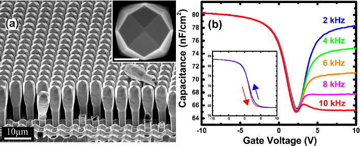
In the quest to achieve Ge-based architectures as loss-less optical components and to resolve the subtleties of the carrier dynamics, we exploit the out-of-equilibrium growth of Ge on deeply patterned Si substrates.Falub et al. (2012) Figure 1(a) demonstrates a scanning electron microscope micrograph of as-grown m-scale crystals developed by depositing 8 m of Ge at by low-energy plasma enhanced chemical vapor depositionRosenblad et al. (1998) onto Si pillars. Such pedestals were separated by 8-m-deep and 3-m-wide trenches patterned onto (001) substrates by optical lithography and reactive ion etching.Falub et al. (2012) The Ge micro-crystals are characterized by a pyramidal top surface bounded by and facets. Such facets stem from a slanted growth front that promptly steers the threading arms towards the lateral sidewalls, where they become pinned. Subsequent material deposition eventually yields a region of the crystal that is completely free from dislocations, although no annealing was performed.Falub et al. (2012); Marzegalli et al. (2013); Isa et al. (2013) Such an approach has been shown to produce space-filling arrays of Ge featuring (i) a giant enhancement in the internal quantum efficiency caused by the removal of dislocations threading through the whole epitaxial layer and (ii) an improved light extraction enabled by total internal reflection at the sidewalls of the micro-crystals. Pezzoli et al. (2014); Isa et al. (2015)
In this letter we utilize dislocation management provided by the Ge micro-crystals while passivating surface traps by means of conformal deposition of dielectric layers. By doing so, we can control and modulate the weight of the nonradiative recombination pathways and gather selective access to the carrier loss occurring either at extended defects or surface states in various temperature regimes. Aside from fruitful applications utilizing Ge as a photonic building block, pinpointing the parasitic sinks of charge carriers provides an in-depth knowledge of the physics of the recombination dynamics at the semiconductor interfaces, which is crucial also as a guide to design advanced semiconductor heterostructures that fulfill ever-demanding photonic and electronic functions.
Surface passivation of the Ge micro-crystals was obtained by growing a high quality thermal layer. Matsubara et al. (2008) The Ge micro-crystal surfaces were first cleaned in acetone followed by rinsing in isopropanol before cyclic hydrofluoric acid / deionized water etching was performed to remove any native oxide films. The Ge micro-crystals were then immediately transferred to a furnace tube oven for thermal oxidation at with gas for 60 min, which results in a thickness of about 20 nm. The was then subsequently capped with 50 nm of unstrained ICP-PECVD .Millar et al. (2015)
To evaluate the quality of the thermally grown , capacitor structures consisting of were fabricated in parallel. Figure 1(b) demonstrates the room temperature capacitance-voltage (C-V) characteristics of the capacitor structures at low frequencies (2-10 kHz). The well behaved threshold voltage response as a function of frequency indicates that there is a low level of interface trapped charge between the and Ge. The inset in Fig. 1(b) shows the high frequency (1 MHz) bidirectional C-V curves. There is no flat-band voltage shift observed from the ideal that was calculated from the work function of Pt ( eV), suggesting there is negligible fixed charge present within the dielectric stack. There is a relatively small flatband voltage hysteresis observed ( mV), which is still consistent with high quality /Ge interfaces.Bellenger et al. (2008); Hirayama et al. (2011) All these observations indicate an efficient electrical passivation of the dangling bonds on the surface of Ge.
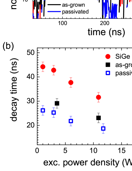
In addition to the C-V investigation, we have also carried out photoluminescence (PL) decay measurements of the indirect band-gap transition to gather direct insights about the effectiveness of the surface passivation on the optical properties of the Ge micro-crystals. The exceedingly long radiative lifetime expected in an indirect gap material such as Ge is typically concealed by the presence of competitive nonradiative events occurring at the defect sites, which appreciably shorten the observable lifetime of minority carriers. Giorgioni et al. (2014) Therefore, time-resolved PL offers us a very sensitive probe of the recombination dynamics and provides a direct method to identify the carrier loss mechanisms.
The samples were placed inside a closed-cycle cryostat at a temperature of 14 K and were excited by the 1064 nm line of a Nd:YAG Q-switched laser. The repetition frequency was 10 kHz with a temporal width of the laser pulse of about 10 ns and an estimated mean power density on the sample surface ranging from 1 to 22.5 . The PL was collected by a single grating monochromator with a spectral bandpass set to 1.5 meV at 0.737 eV, which corresponds to the highest energy peak of the indirect gap PL band, as clarified by low temperature continuous-wave PL data of the as-grown sample shown in the inset of Fig. 2. The emission was detected by a photomultiplier tube (PMT) operated in a single photon counting mode with a precision for the time decay of 0.3 ns. It should be noted that the weakening of the PL signal and the spectral position of the emission energy, being close to the detectivity cut-off of the PMT, prevented us from reliably implement time decay measurements above cryogenic temperatures.
A well-defined exponential decay can be observed in Fig. 2(a). Surprisingly, the decay curves for both the as-grown and passivated samples demonstrate a similar slope, that is a comparable lifetime for electrons residing in the -valley. The measured decay times, summarized in Fig. 2(b), approach 30 ns and decrease by increasing the excitation power density, as a result of the local heating of the sample caused by the pulsed excitation. The negligible effect of the oxide coating on the carrier lifetime clearly demonstrates that, despite the large surface-to-volume ratio of the Ge micro-crystals, surface traps are not likely to limit the low temperature emission. This observation suggests the existence of competing mechanisms that are more effective than surface states in the capture of the injected carriers.
To provide insight into the origin of such parasitic recombination, we introduce a sample that mimics the un-passivated, as-grown Ge micro-crystals except it encapsulates three additional films at 2, 4 and 6 m from the top surface, each with a thickness of 10 nm. The strain and Ge molar fractions have been suitably designed in order to provide a band off-set between the alloy layers and the Ge matrix that impedes the diffusion of the photogenerated carriers towards the defective Ge/Si interface. Pezzoli et al. (2014)
Remarkably, the insertion of the SiGe barriers yields the slowest decay among those reported in Fig. 2(a) lengthening the electron lifetime up to ns [see Fig. 2(b)]. This exceeds the literature data reported for Ge on Si heterostructures, Sukhdeo et al. (2016); Sheng et al. (2013); Geiger et al. (2014); Nam et al. (2014) and provides the first direct proof put forward in any recent work,Pezzoli et al. (2014) that band-gap engineered SiGe/Ge architectures are effective in mitigating the optical activity of buried dislocations.
At higher lattice temperatures, dislocations are nevertheless expected to play a less prominent role because of the augmented ionization probability of their associated localized energy levels. To clarify this physical picture we carried out additional PL measurements by using the 1.165 eV line of a CW Nd: laser. The exciting power density was about 1 and the emission was analyzed using a Fourier transform spectrometer equipped with Peltier cooled PbS detector.
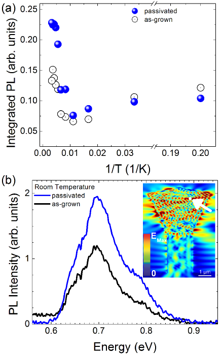
Figure 3(a) reports a notable deviation from the standard temperature dependent PL quenching. As the lattice temperature increases, there exists a sharp threshold above which a marked strengthening of the emission for both the as-grown and passivated sample can be observed. Such PL behavior is a hallmark of valley repopulation induced by thermal emission of carriers from the defect sites.Pezzoli et al. (2014); Figielski (1978) It should be noted, however, that the passivation results in a strong increase in the high temperature regime, yielding a room temperature PL spectrum with nearly twice the emission intensity of the as-grown Ge micro-crystals. This result demonstrates the effectiveness of the oxide coating in mitigating the nonradiative capture by surface states and it reconciles the optical investigation with the results of the electrical characterization discussed above.
Finally, in order to study the possible role of the oxide as an anti-reflection coating and to clarify whether the room temperature PL enhancement is affected by photonic effects, e.g. Purcell’s effect, we benchmarked our experimental data against finite-difference time-domain simulations.Pezzoli et al. (2014); FDTD Solutions, version 8.5.3; Lumerical Solutions, Inc.: Canada, (2013); Celebrano et al. (2015) The steady-state PL process is mimicked by combining three simulation steps: (i) absorption of light by the Ge micro-crystals at the pump energy; (ii) local incoherent emission due to the recombination of electron-hole dipoles; and (iii) propagation of the emitted photons to the far field and their detection within the collection angle of the optics.Celebrano et al. (2015) For the first step, we simulated the illumination of the Ge micro-crystals array with a Gaussian beam at 1.165 eV with an incidence angle resembling the actual experimental geometry. We then numerically evaluated the net flux of the Poynting vector entering the Ge micro-crystals and determined the total power absorption. As a second step, in order to mimic the incoherent emission process, we ran about 100 independent simulations, each one with a different randomly-oriented and randomly-located emitting dipole inside the Ge micro-crystals with a bandwidth covering the spectral range between 0.89 and 0.62 eV (i.e., both direct- and indirect-band emission from Ge). Such a large number of single-dipole simulations is needed in order to avoid spurious interference effects between different emitting dipoles, something that would have no counterpart in the actual PL process due to the lack of coherence. One representative field map resulting from such simulations is demonstrated in the inset of Fig. 3(b). Finally, we projected the local field distribution generated by each dipole to the far field and integrated the power flux within the collection angle of the optics to get an estimate of the emitted power.
By doing so, we are in the position to calculate the ratio between the expected PL intensity collected from the as-grown and passivated Ge micro-crystals under the same illumination conditions. We find that the difference in the PL intensity between the two systems is within 1-2%, i.e. well below the experimentally observed effects. This confirms that the PL enhancement demonstrated in Fig. 3(b) must be ascribed to an improvement of the internal quantum efficiency, which stems from the reduced nonradiative recombination at the passivated sidewalls of the micro-crystals.
In conclusion, we identified a viable approach to disentangle nonradiative transitions due to dislocations and surface states and gather insights about the complex kinetics of the recombination processes in Ge on Si heterostructures. We demonstrated the prominent role of dislocations at low temperature and the surge of room temperature PL emission under a suitable surface passivation. These findings can be used for engineering defects in key photonic building blocks such as lasers, optical resonator, and photodetectors fabricated in group IV materials. It is worth noting that our investigation can be extended to the epitaxial growth directly on silicon of other highly mismatched materials, thus enlarging even further the Si photonic toolbox.
We are grateful to the technical staff at the LNESS laboratory in Como and FIRST clean room at ETH Zuerich. We acknowledge support from Fondazione Cariplo through Grant No. 2013-0623, the Sinergia project NOVIPIX CRSII2_147639 of the Swiss National Science Foundation and Pilegrowth Tech srl for technical support.
References
- Leuthold et al. (2010) J. Leuthold, C. Koos, and W. Freude, Nature Photon. 4, 535 (2010).
- Dai et al. (2012) D. Dai, J. Bauters, and J. E. Bowers, Light: Science & Applications 1, e1 (2012).
- Lim et al. (2014) A. E.-J. Lim, J. Song, Q. Fang, C. Li, X. Tu, N. Duan, K. K. Chen, R. P.-C. Tern, and T.-Y. Liow, IEEE J. Sel. Top. Quant. 20, 8300112 (2014).
- Pillarisetty (2011) R. Pillarisetty, Nature 479, 324 (2011).
- Pezzoli et al. (2013) F. Pezzoli, L. Qing, A. Giorgioni, G. Isella, E. Grilli, M. Guzzi, and H. Dery, Phys. Rev. B 88, 045204 (2013).
- Michel et al. (2010) J. Michel, J. F. Liu, and L. C. Kimerling, Nature Photon. 4, 527 (2010).
- Liang and Bowers (2010) D. Liang and J. E. Bowers, Nature Photon. 4, 511 (2010).
- Baldassarre et al. (2015) L. Baldassarre, E. Sakat, J. Frigerio, A. Samarelli, K. Gallacher, E. Calandrini, G. Isella, D. J. Paul, M. Ortolani, and P. Biagioni, Nano Lett. 15, 7225 (2015).
- Paul (2004) D. J. Paul, Semicond. Sci. Technol. 19, R75 (2004).
- Liu et al. (2010) J. Liu, X. Sun, R. Camacho-Aguilera, L. C. Kimerling, and J. Michel, Opt. Lett. 35, 679 (2010).
- Camacho-Aguilera et al. (2012) R. E. Camacho-Aguilera, Y. Cai, N. Patel, J. T. Bessette, M. Romagnoli, L. C. Kimerling, and J. Michel, Opt. Express 20, 11316 (2012).
- Wirths et al. (2015) S. Wirths, R. Geiger, N. von den Driesch, G. Mussler, T. Stoica, S.Mantl, Z. Ikonic, M. Luysberg, S. Chiussi, J. M. Hartmann, H. Sigg, J. Faist, D. Buca, and D. Grützmacher, Nature Photon. 9, 88 (2015).
- Yang et al. (2003) V. K. Yang, M. Groenert, C. W. Leitz, A. J. Pitera, M. T. Currie, and E. A. Fitzgerald, J. Appl. Phys. 93, 3859 (2003).
- Sukhdeo et al. (2016) D. S. Sukhdeo, S. Gupta, K. C. Saraswat, B. R. Dutt, and D. Nam, Opt. Commun. 364, 233 (2016).
- (15) X. Li, Z. Li, S. Li, L. Chrostowski, and G. Xia, arXiv:1511.05972 .
- Falub et al. (2012) C. V. Falub, H. von Känel, F. Isa, R. Bergamaschini, A. Marzegalli, D. Chrastina, G. Isella, E. Müller, P. Niedermann, and L. Miglio, Science 335, 6074 (2012).
- Rosenblad et al. (1998) C. Rosenblad, H. R. Deller, A. Dommann, T. Meyer, P. Schröter, and H. von Känel, J. Vac. Sci. Technol. A 16, 2785 (1998).
- Marzegalli et al. (2013) A. Marzegalli, F. Isa, H. Groiss, E. Müller, C. V. Falub, A. G. Taboada, P. Niedermann, G. Isella, F. Schäffler, F. Montalenti, H. von Känel, and M. Leo, Adv. Mater. 25, 4408 (2013).
- Isa et al. (2013) F. Isa, A. Marzegalli, A. G. Taboada, C. V. Falub, G. Isella, F. Montalenti, H. von Känel, and L. Miglio, APL Materials 1, 052109 (2013).
- Pezzoli et al. (2014) F. Pezzoli, F. Isa, G. Isella, C. V. Falub, T. Kreiliger, M. Salvalaglio, R. Bergamaschini, E. Grilli, M. Guzzi, H. von Känel, and L. Miglio, Phys. Rev. Appl. 1, 044005 (2014).
- Isa et al. (2015) F. Isa, F. Pezzoli, G. Isella, M. Meduňa, C. V. Falub, E. Müller, T. Kreiliger, A. G. Taboada, H. von Känel, and L. Miglio, Semicond. Sci. Technol. 30, 105001 (2015).
- Matsubara et al. (2008) H. Matsubara, T. Sasada, M. Takenaka, and S. Takagi, Appl. Phys Lett. 93, 032104 (2008).
- Millar et al. (2015) R. W. Millar, K. Gallacher, A. Samarelli, J. Frigerio, D. Chrastina, G. Isella, T. Dieing, and D. J. Paul, Opt. Express 23, 18193 (2015).
- Bellenger et al. (2008) F. Bellenger, M. Houssa, A. Delabie, V. Afanasiev, T. Conard, M. Caymax, M. Meuris, K. D. Meyer, and M. M. Heyns, J. Electrochem Soc. 155, G33 (2008).
- Hirayama et al. (2011) K. Hirayama, K. Yoshino, R. Ueno, Y. Iwamura, H. Yang, D. Wang, and H. Nakashima, Solid State Electron. 60, 122 (2011).
- Giorgioni et al. (2014) A. Giorgioni, E. Vitiello, E. Grilli, M. Guzzi, and F. Pezzoli, Appl. Phys. Lett. 105, 152404 (2014).
- Sheng et al. (2013) J. J. Sheng, D. Leonhardt, S. M. Han, S. W. Johnston, J. G. Cederberg, and M. S. Carroll, J. Vac. Sci. Technol. B 31, 051201 (2013).
- Geiger et al. (2014) R. Geiger, J. Frigerio, M. J. Süess, D. Chrastina, G. Isella, R. Spolenak, J. Faist, and H. Sigg, Appl. Phys. Lett. 104, 062106 (2014).
- Nam et al. (2014) D. Nam, J. H. Kang, M. L. Brongersma, and K. C. Saraswat, Opt. Lett. 39, 6205 (2014).
- Figielski (1978) T. Figielski, Solid-State Electron. 21, 1403 (1978).
- FDTD Solutions, version 8.5.3; Lumerical Solutions, Inc.: Canada, (2013) FDTD Solutions, version 8.5.3; Lumerical Solutions, Inc.: Canada, 2013, .
- Celebrano et al. (2015) M. Celebrano, M. Baselli, M. Bollani, J. Frigerio, A. B. Shehata, A. D. Frera, A. Tosi, A. Farina, F. Pezzoli, J. Osmond, X. Wu, B. Hecht, R. Sordan, D. Chrastina, G. Isella, L. Duó, M. Finazzi, and P. Biagioni, ACS Photonics 2, 53 (2015).