On the widths of Stokes lines in Raman scattering from molecules adsorbed at metal surfaces and in molecular conduction junctions
Abstract
Within a generic model we analyze the Stokes linewidth in surface enhanced Raman scattering (SERS) from molecules embedded as bridges in molecular junctions. We identify four main contributions to the off-resonant Stokes signal and show that under zero voltage bias (a situation pertaining also to standard SERS experiments) and at low bias junctions only one of these contributions is pronounced. The linewidth of this component is determined by the molecular vibrational relaxation rate, which is dominated by interactions with the essentially bosonic thermal environment when the relevant molecular electronic energy is far from the metal(s) Fermi energy(ies). It increases when the molecular electronic level is close to the metal Fermi level so that an additional vibrational relaxation channel due to electron-hole (eh) excition in the molecule opens. Other contributions to the Raman signal, of considerably broader linewidths, can become important at larger junction bias.
I Introduction
Molecular optoelectronics is an active field of research made possible by advances in laser technology and nanofabrication.Galperin and Nitzan (2012) The possibility to conduct optical measurements in open non-equilibrium nano-systems resulted in the appearance of new diagnostic tools, and offers a route to optical control schemes such as switching in molecular electronics devices. Standard observables of optical spectroscopy can yield new information when monitored in open current-carrying molecular junctions. For example, current-induced fluorescenceWu et al. (2008); Chen et al. (2010) yields information on molecular resonances in the non-equilibrium system and makes imaging at submolecular resolution feasible, while the intensity of the emitted light corresponds to charge current noise at optical frequenciesSchneider et al. (2010, 2012) and can yield information on fast voltage transients at the tunnel junction.Grosse et al. (2013) Raman spectroscopy of current-carrying junctions can serve as a diagnostic tool similar to inelastic tunneling spectroscopy, and as an indicator for current-induced heating of electronic and vibrational degrees of freedom.Ioffe et al. (2008); Ward et al. (2008, 2011) (Possible pitfalls of such characterization were discussed theoretically Galperin and Nitzan (2011a, b)). Recently, measurements of dc current and/or noise in response to laser pulse pair sequence was suggested as a variant of pump-probe spectroscopy for molecular junctions capable of providing information on intra-molecular dynamics at sup-picosecond timescale.Selzer and Peskin (2013); Ochoa et al. (2015)
As noted above, the ability to characterize vibrational structure of a molecular device makes Raman scattering similar to inelastic electron tunneling spectroscopy (IETS). The corresponding spectra are characterized by their peak positions and heights, as well as lineshapes and linewidths. In addition to standard peaks, rich IETS lineshape features caused by interference between elastic and inelastic scattering channels are known.Galperin et al. (2004a); Rai and Galperin (2012) Similar interference features in Raman scattering were recently discussed.Dey et al. (2016) The dependence of (resonant) IETS spectra on gate and source-drain biases was measured and discussed.Park et al. (2000); Pasupathy et al. (2005); Chae et al. (2006) It appears to primarily manifest the sensitivity of molecular normal modes to the molecule charging state.Galperin et al. (2008); White and Galperin (2012) Similarly, a shift in the frequencies of Stokes lines with bias was observedWard et al. (2011); Natelson et al. (2013) and was shown to result at least partly from the voltage dependence of the charge on the molecule.Kaasbjerg et al. (2013); Li et al. (2014); White et al. (2014a, b) Finally, the linewidths of IETS signals where studied both experimentallyWang et al. (2004) and theoreticallyGalperin et al. (2004b) and were shown to be dominated by the strength of electron-phonon interactions. No such study has been done so far for Raman scattering from molecular junctions.
The present paper focuses on the latter issue: we identify the main contribution to the observed Raman intensity and analyze, using a generic model, the non-monotonic dependence of the Stokes linewidth on the gate and bias potentials. In Section II we introduce our model for an illuminated molecular junction as well as our calculation methodology for off-resonant Raman scattering from this system. Section III presents our results and Section IV concludes.
II Model and Method
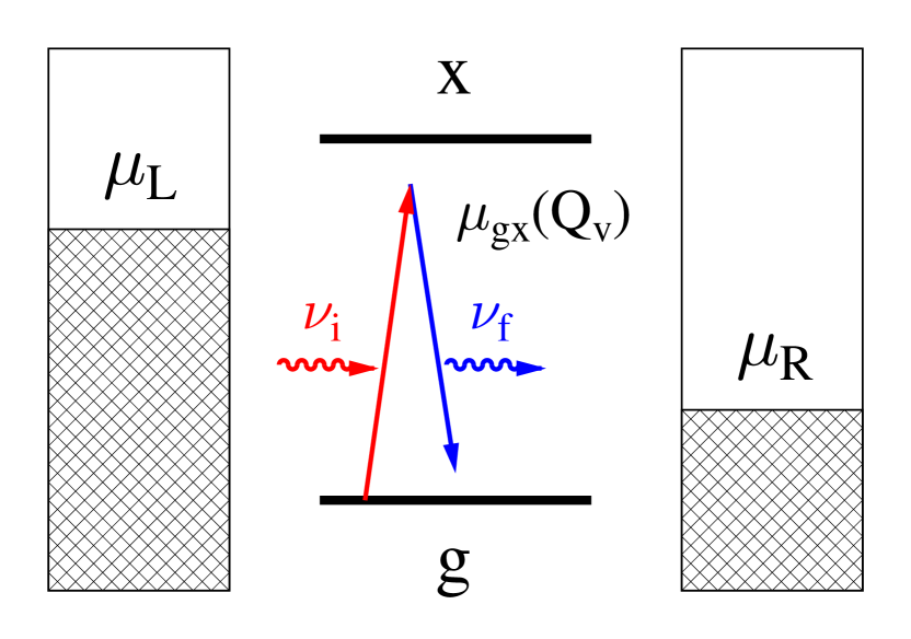
We consider junction comprised of a molecule coupled to two metallic contacts, and , each at its own equilibrium. The molecule is represented by two electronic levels (ground, , and excited, , states) and a molecular vibration, taken harmonic of frequency , linearly coupled to the levels populations (an Holstein-type model). The junction is subjected to an external radiation field, represented by a set of quantum harmonic modes (see sketch in Fig. 1). One of these modes, of frequency represent the incident mode that pumps the system. All other modes, , are taken to be vacant. The Hamiltonian is
| (1) |
where represents the dark junction, is Hamiltonian of the radiation field, and is the molecule-field coupling. Explicitly
| (2) | ||||
| (3) | ||||
| (4) |
Here () and () create (annihilate) electrons in the molecular level and state of the metal contacts, respectively. and are the corresponding electron number operators for states () of the molecule and of the contacts. and are molecular excitation and de-excitation operators. () and () create (annihilate) vibrational quanta in the molecule and mode of the thermal bath, respectively. and are the oscillators position operators. () creates (destroys) photon in the mode of radiation field. Note that this model contains two interactions that can cause inelastic light scattering. First is the dependence of the molecule-field coupling on the vibrational coordinate. The other is the polaronic coupling term in Eq.(II) whose importance is measured by the electron-vibration coupling .
Following Refs. Galperin et al. (2009a, b) and focusing on the low voltage bias regime, we consider only ‘normal Raman’ scattering, i.e. a process where the initial state is its ground state.111For strongly biased junctions both lower and upper molecular states may be partially occupied, giving rise to more contributions to elastic and inelastic light scattering, see Ref. Galperin et al. (2009b).
Raman scattering is a coherent process of fourth order in the matter-radiation field coupling (two orders correspond to the outgoing photon, blue line in Fig. 1, and two orders correspond to the incoming photon, red line in Fig. 1). Explicit steady-state expression for the ‘normal Raman’ scattering from the initial mode to a final mode of the radiation field is (see Ref. Galperin et al. (2009b) for details)
| (5) | ||||
where . As in standard treatments, we expand the molecule-field coupling to linear term in Taylor series in the molecular vibrational displacement
| (6) |
Depending on combination of molecule-field coupling terms ( or ) in the expression (II) one gets contributions to vibrational and electronic Raman (Rayleigh) scatterings. For example, substituting only in place of all molecule-field couplings in Eq.(II) yields the pure electronic Raman contribution discussed in Refs. Galperin and Nitzan (2011a, b). Here we focus on the vibrational Raman scattering, whose lowest order contribution comes from terms that are second order in the coupling to the molecular vibration. Such terms will be of order . After collecting all such contributions to the vibrational Raman we (a) separate vibrational and electronic degrees of freedom (i.e. neglecting vibration-induced electronic correlations) and (b) neglect electronic correlation between ground and excited states of the molecule assuming that the energy gap between them is much larger than the widths associated with their coupling to the contacts. We focus on off-resonant Raman scattering and restrict our consideration to gate voltages that keep the upper electronic level above the leads chemical potentials (so it is essentially unpopulated), Under these approximations the explicit expression becomes
| (7a) | ||||
| (7b) | ||||
| (7c) | ||||
| (7d) | ||||
Here , (), and are Fourier transforms of the greater/lesser/retarded projections of the single electron Green function and the greater projection of the phonon Green function, respectively
| (8) | ||||
| (9) |
where is the contour ordering operator. is the density of optical modes.
Next, some simplification can be made by invoking the reasonable assumption that the molecule-contacts coupling is much larger than the molecule-radiation field coupling as well as the electron-phonon interaction. Under this assumption we can disregard the latter interactions in the expressions for the electronic Green functions, taking the forms that correspond to a molecule coupled to the two metal leads
| (10) | ||||
| (11) | ||||
| (12) |
Here (, ) is electron escape rate from level into contact , , is the Fermi-Dirac thermal distribution in contact .
For the evaluation of the phonon Green functions we again disregard the molecule-radiation field coupling, but keep the electron-phonon interaction. This leads to
| (13) | ||||
| (14) |
We will henceforth assume that and use to access the region. In Eqs. (13) and (14) ,
| (15) |
is the retarded projection of free phonon Green function, and
| (16) | ||||
| (17) | ||||
| (18) |
are the projections of the self-energy of the molecular vibration due to its coupling to the (bosonic) white thermal bath. Here is the Bose-Einstein thermal distribution and is the dissipation rate of molecular vibrational excitation due to coupling to thermal bath. The self energy of the molecular phonon associated with the electron-vibration coupling is treated at the level of the Born approximation
| (19) | ||||
| (20) | ||||
| (21) |
Before describing our numerical results, it is important to note the different physical origins of the four contributions, Eqs. (7)-(7d), to the Raman signal, that can be inferred from the different forms of the electronic Green functions appearing in them and the forms of the corresponding energy denominators. It is convenient to look at them in comparison to the pure electronic Raman components discussed in Ref. Galperin and Nitzan (2011b) (see Fig. 2 in this reference). Without the vibrational shift the contribution (7) with would be the Rayleigh line where each scattering event involves a single electron-hole pair - an occupied electronic level near and an empty electronic level near . The contribution (7b) with if considered without the vibrational shift corresponds to that contribution to the pure electronic Raman scattering where the difference between the initial and final photon energy is expressed by moving an electron between two metal levels close to , requiring one of these levels to be occupied and the other empty. The term (7c) that depends on is similar, except that the difference between incoming and outgoing photons is expressed in electron motion between two levels near , again requiring one of them to be occupied and the other empty. Finally, the contribution (7d) that contains splits the photon energy difference between two electronic transitions, one near and the other near .
Two observations follow, still on this qualitative level: First, in equilibrium and at low bias, in the common situation where the lower and upper electronic orbitals are far below and far above the metal(s) Fermi energy(ies) respectively, Eq. (7) will be the dominant contribution to the vibrational Raman signal. Second, the vibrational Raman lines associated with this contribution will be narrow in the sense that their width will not reflect the excitation of electron-hole pairs in the metal. The contributions (7b) and (7c) will be important in situations where, respectively, and are close to the metals Fermi energies. Furthermore, these contributions will be considerable broader, reflecting the excitation of electron-hole pairs in the metal alongside the vibrational excitation. Note that at low temperatures this broadening will be asymmetric, corresponding to an electronic side-band of the vibrational Raman transition as recently discussed in Ref. Dey et al. (2016). Finally, we expect that also the pure vibrational Raman spectrum associated with Eq. (7) will be broader when one of the the molecular electronic levels is close to the Fermi energy, because of the increased importance of the electronic relaxation channel for the molecular vibration in this situation.Kaasbjerg et al. (2013)
III Numerical results
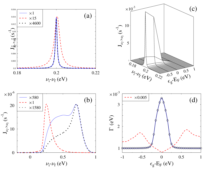
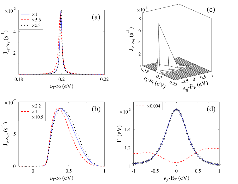
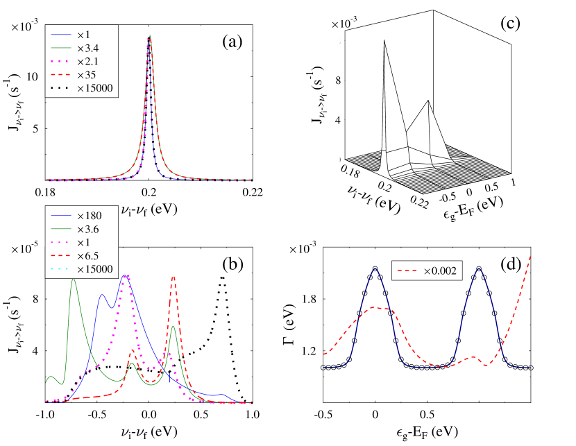
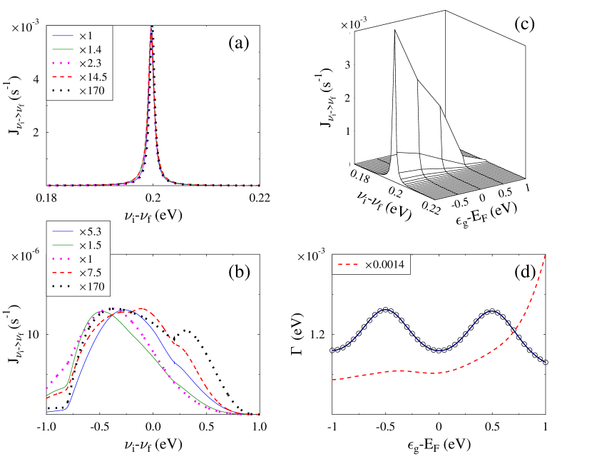
Here we present numerical results for the Raman flux, Eq. (7), for the model (1)-(4). Below we focus on the most prominent contributions, Eqs. (7) and (7b). The following parameters are used in these calculations: K, eV (the absolute level positions are varied as described below), eV (in Figs. 2 and 4) and eV (in Figs. 3 and 5), (), eV, eV, and eV. The Fermi energy is chosen as the origin, , and the bias is applied symmetrically and . The incident frequency is taken as eV, which corresponds for the present choice of molecular parameters to off-resonant Raman scattering. The couplings to the radiation field are assumed to satisfy eV. The optical resolution windows of the incident energy and measuring device, and in Eq. (7), are taken to be the same, . The calculations were performed on an energy grid spanning the range from to eV with step size eV.
We envision an experiment in which the position of the molecular resonances can be changed by a gate voltage. We start from the situation where level is far below the Fermi energy and level is far above it, so that the lower level is occupied and upper one is empty, and consider the effect on the Raman spectrum of applying a gate voltage to move to the vicinity of, and then beyond, the chemical potentials. In this regime the two main contributions to the Raman flux are given by Eqs. (7) and (7b) with the first one dominating the intensity of the Stokes line. (As explained above, the terms (7c) and (7d) are potentially important only when the excited state is populated). The Raman linewidths reported below are estimated using the standard deviation associated with the corresponding Raman peak calculated on the employed energy grid.
Figure 2 shows results of of this calculation for the equilibrium case, . Note that the intensity of the Stokes line decreases with decrease of the population in the ground state (see Fig. 2c), however the implication of this observation should be understood with respect to the 2-level model used here. In reality, when goes up and above the metal Fermi energy, other lower molecular levels will contribute to the Raman signal. Disregarding this issue, the following additional observations can be made:
-
1.
The dominant Raman feature is indeed that associated with contribution (7) the electronically elastic/vibrationally inelastic signal. The contribution (7b) becomes comparable when is near the metal Fermi energy. It should be kept in mind that and additional broad feature, the electronically inelastic/vibrationally elastic (pure electronic) is not displayed in these figures. In experimental spectra, the signal (7b) may often become part of this broad electronic background.
- 2.
- 3.
-
4.
Comparing the results displayed in Figures 2 and 3 (small and large molecule-metal coupling (), respectively, we note that the dominant low bias feature, namely the contribution (7) is essentially the same in both cases. Interestingly, when is at the Fermi energy (dashed red lines in Figs. 2a and 3a), this feature is broader in the smaller case. This is also seen in comparing Figs. 2d and 3d. This behavior reflects the fact that when , even when , most of the electronic spectral density (of width ) is outside the region of partial electronic occupation ( where f is the Fermi distribution) in which the electronic channel for vibrational relaxation is open. The fact that the spectra in Fig. 3 are smoother and less structured than in Fig. 2 similarly reflects the fact that for large all behaviors associated with the position of relative to and the width of the partially populated region are smoothened.
The width of the vibrational Raman lines reflects three types of contributions. First there is the relaxation to the thermal bosonic environment that is not affected (in our model) by the bias and gate potentials. Second is the additional relaxation channel due to electron-vibration coupling, that can dominate the overall width when the molecular electronic level approaches the metal Fermi level. The structure of this contribution suggests that the width of the term (7) (solid line in Fig. 2d) is dominated by the (renormalized) density of molecular vibration (circles in Fig. 2d). Finally, as discussed above, there is the electron-hole sideband that appears prominently in the term (7b) (as well as (7c) and (7d)). Note again that in actual observations it will not be easy to distinguish between this sideband to the vibrational transition and the underlying Raman continuum that originates primarily from the pure electronic Raman scattering.Galperin and Nitzan (2011b)
We now turn to the nonequilibrium situation with eV and eV. The total Stokes intensity is here affected by two factors: the population of the lower level and the current induced heating of the molecular vibration. As a result, the decrease in the Stokes intensity when approaches the lowest chemical potential due to depletion of the level population changes to increase in the intensity when the level is in the bias window (nonequilibrium feature) - see Fig. 4c. The width of the dominant contribution (7) shows similar behavior as in the equilibrium case, with increase of the width resulting from opening the electronic relaxation channel when approaches the metal Fermi energies. This contribution to the width is again symmetric about each of the Fermi energies (see Figs. 4a and 3d). In contrast, the nonequilibrium electronic distribution, in particular the existence of two energy regions of partial populations of metal electronic states, causes drastic changes and more structure in both lineshape (Fig. 4b) and linewidth (Fig. 3d) of the contribution (7b) as compared to equilibrium case. This structure is again smoothened in the large case (Fig. 5). Still, since this peak is much lower and broader than that of (7), it may be considered as part of the electronic Raman background.
IV Conclusion
Within a simple two-level model of a molecular junction we consider off-resonant Raman scattering and discuss dependence of Stokes linewidth on gate and bias voltages. We focus on low bias regime, where upper level is almost empty, and thus consider only ‘normal Raman’ contribution to the total signal (i.e. Raman scattering which originates at the lower molecular level). Employing realistic parameters we show that the linewidth changes non-monotonically with gate voltage demonstrating maximum at resonance between molecular level and chemical potential(s) of metallic contacts. Analysis shows that the effect is due to opening of an electronic relaxation channel for molecular vibrations by which e-h excitations are formed in metallic contacts. At low biases and for realistic parameters this mechanism is the dominant contribution to the Stokes linewidth. Other mechanisms are relaxation of molecular vibration due to coupling to the thermal environment and surface plasmons. The latter was not included in the consideration due to mismatch between characteristic plasmons and molecular vibrations frequencies. Note that the model also disregards inhomogeneous broadening and pure dephasing contributions. Experimental verification of our theoretical prediction seems to be a realistic possibility.
Acknowledgements.
The research of AN is partially supported by the Israel Science Foundation and the US-Israel Binational Science Foundation. MG gratefully acknowledges support by the US Department of Energy.References
- Galperin and Nitzan (2012) M. Galperin and A. Nitzan, Phys. Chem. Chem. Phys. 14, 9421 (2012).
- Wu et al. (2008) S. W. Wu, G. V. Nazin, and W. Ho, Phys. Rev. B 77, 205430 (2008).
- Chen et al. (2010) C. Chen, P. Chu, C. A. Bobisch, D. L. Mills, and W. Ho, Phys. Rev. Lett. 105, 217402 (2010).
- Schneider et al. (2010) N. L. Schneider, G. Schull, and R. Berndt, Phys. Rev. Lett. 105, 026601 (2010).
- Schneider et al. (2012) N. L. Schneider, J. T. Lü, M. Brandbyge, and R. Berndt, Phys. Rev. Lett. 109, 186601 (2012).
- Grosse et al. (2013) C. Grosse, M. Etzkorn, K. Kuhnke, S. Loth, and K. Kern, Appl. Phys. Lett. 103, 183108 (2013).
- Ioffe et al. (2008) Z. Ioffe, T. Shamai, A. Ophir, G. Noy, I. Yutsis, K. Kfir, O. Cheshnovsky, and Y. Selzer, Nature Nanotech. 3, 727 (2008).
- Ward et al. (2008) D. R. Ward, N. J. Halas, J. W. Ciszek, J. M. Tour, Y. Wu, P. Nordlander, and D. Natelson, Nano Lett. 8, 919 (2008).
- Ward et al. (2011) D. R. Ward, D. A. Corley, J. M. Tour, and D. Natelson, Nature Nanotech. 6, 33 (2011).
- Galperin and Nitzan (2011a) M. Galperin and A. Nitzan, J. Phys. Chem. Lett. 2, 2110 (2011a).
- Galperin and Nitzan (2011b) M. Galperin and A. Nitzan, Phys. Rev. B 84, 195325 (2011b).
- Selzer and Peskin (2013) Y. Selzer and U. Peskin, J. Phys. Chem. C 117, 22369 (2013).
- Ochoa et al. (2015) M. A. Ochoa, Y. Selzer, U. Peskin, and M. Galperin, J. Phys. Chem. Lett. 6, 470 (2015).
- Galperin et al. (2004a) M. Galperin, M. A. Ratner, and A. Nitzan, J. Chem. Phys. 121, 11965 (2004a).
- Rai and Galperin (2012) D. Rai and M. Galperin, Phys. Rev. B 86, 045420 (2012).
- Dey et al. (2016) S. Dey, M. Banik, E. Hulkko, K. Rodriguez, V. A. Apkarian, M. Galperin, and A. Nitzan, Phys. Rev. B 93, 035411 (2016).
- Park et al. (2000) H. Park, J. Park, A. K. L. Lim, E. H. Anderson, A. P. Alivisatos, and P. L. McEuen, Nature 407, 57 (2000).
- Pasupathy et al. (2005) A. N. Pasupathy, J. Park, C. Chang, A. V. Soldatov, S. Lebedkin, R. C. Bialczak, J. E. Grose, L. A. K. Donev, J. P. Sethna, D. C. Ralph, and P. L. McEuen, Nano Lett. 5, 203 (2005).
- Chae et al. (2006) D.-H. Chae, J. F. Berry, S. Jung, F. A. Cotton, C. A. Murillo, and Z. Yao, Nano Lett. 6, 165 (2006).
- Galperin et al. (2008) M. Galperin, A. Nitzan, and M. A. Ratner, Phys. Rev. B 78, 125320 (2008).
- White and Galperin (2012) A. J. White and M. Galperin, Phys. Chem. Chem. Phys. 14, 13809 (2012).
- Natelson et al. (2013) D. Natelson, Y. Li, and J. B. Herzog, Phys. Chem. Chem. Phys. 15, 5262 (2013).
- Kaasbjerg et al. (2013) K. Kaasbjerg, T. Novotný, and A. Nitzan, Phys. Rev. B 88, 201405 (2013).
- Li et al. (2014) Y. Li, P. Doak, L. Kronik, J. B. Neaton, and D. Natelson, Proc. Natl. Acad. Sci. 111, 1282 (2014).
- White et al. (2014a) A. J. White, S. Tretiak, and M. Galperin, Nano Lett. 14, 699 (2014a).
- White et al. (2014b) A. J. White, M. A. Ochoa, and M. Galperin, J. Phys. Chem. C 118, 11159 (2014b).
- Wang et al. (2004) W. Wang, T. Lee, I. Kretzschmar, and M. A. Reed, Nano Lett. 4, 643 646 (2004).
- Galperin et al. (2004b) M. Galperin, M. A. Ratner, and A. Nitzan, Nano Lett. 4, 1605 (2004b).
- Galperin et al. (2009a) M. Galperin, M. A. Ratner, and A. Nitzan, Nano Lett. 9, 758 (2009a).
- Galperin et al. (2009b) M. Galperin, M. A. Ratner, and A. Nitzan, J. Chem. Phys. 130, 144109 (2009b).
- Note (1) For strongly biased junctions both lower and upper molecular states may be partially occupied, giving rise to more contributions to elastic and inelastic light scattering, see Ref. Galperin et al. (2009b).