Interference features in scanning gate conductance maps of quantum point contacts with disorder
Abstract
We consider quantum point contacts (QPCs) defined within disordered two-dimensional electron gases as studied by scanning gate microscopy. We evaluate the conductance maps in the Landauer approach and wave function picture of electron transport for samples with both low and high electron mobility at finite temperatures. We discuss the spatial distribution of the impurities in the context of the branched electron flow. We reproduce the surprising temperature stability of the experimental interference fringes far from the QPC. Next, we discuss – previously undescribed – funnel-shaped features that accompany splitting of the branches visible in previous experiments. Finally, we study elliptical interference fringes formed by an interplay of scattering by the point-like impurities and by the scanning probe. We discuss the details of the elliptical features as functions of the tip voltage and the temperature, showing that the first interference fringe is very robust against the thermal widening of the Fermi level. We present a simple analytical model that allows for extraction of the impurity positions and the electron gas depletion radius induced by the negatively charged tip of the atomic force microscope, and apply this model on experimental scanning gate images showing such elliptical fringes.
I Introduction
Scanning gate microscopy (SGM) is an experimental technique which probes transport properties of systems based on a two-dimensional electron gas (2DEG) using the charged probe of an atomic force microscope (AFM) Eriksson1996 ; Sellier2011 ; Ferry2011 . A negatively charged AFM tip induces a finite size depletion in the 2DEG, which acts as a movable scatterer of size and location controlled by the voltage applied to the SGM tip and its position above the sample Brun2014 . The SGM technique was used first to investigate the electron transport in quantum point contacts (QPCs) Wees1988 . The SGM conductance maps recorded as a function of the tip position in the vicinity of a QPC contain two characteristic features (i) interference fringes with oscillation period equal to half the Fermi wavelength Topinka2000 ; Topinka2001 ; Kozikov2015 ; Jura2007 ; Jura2009 ; Kumar2013 and (ii) semiclassical branched flow of electron trajectories Heller2003 ; Liu2013 ; Liu2015 ; Jura2007 . The fringes (i) arise from the coherent interference between the electron waves incident from the QPC and backscattered by the SGM tip Kolasinski2014Slit ; Jura2007 . The branched flow (ii) stems from the smooth potential disorder in the high mobility semiconductor structures Jura2007 . For low-mobility samples the hard-impurity scattering is dominant and leads to coherent fringes which are surprisingly thermally stable, with the interference pattern visible at a distance from the QPC which largely exceeds the thermal length Topinka2000 ; Topinka2001 ; Jura2007 . This surprising behavior is explained Topinka2000 ; Topinka2001 ; Jura2007 by coherent scattering involving the tip and nearby impurities spaced by a distance below .
In this paper we consider numerical simulations of a coherent branched flow of electrons spreading from a QPC into the 2DEG. We study the effect of smooth and hard impurities on the transport for both low and high density of scatterers, i.e. for high and low mobility samples, respectively. For low mobility samples most of the features visible in the experimental SGM images can be explained in terms of a 1D model of the branch, including (i) thermally persistent fringes visible at K, (ii) reappearance of fringes in some part of SGM images far from the QPC, (iii) perpendicular alignment of the fringes to the branch direction, (iv) frequency of the fringes near the impurities that changes with . We discuss splittings of the branches at some defects and a funnel shaped features that accompany the splitting.
We also consider high mobility samples and indicate by both experiment and theory distinct signatures of a few hard scatterers present within the system that produce pronounced elliptical features in the SGM conductance maps. These elliptical features – never previously described – result from interference involving both the scatterer and the tip and remain stable up to at least K. We provide a simple model to describe these nearly elliptical contours which allows one to indicate the position of the scatterer within the sample, and the size of the area depleted by the tip.
II Model
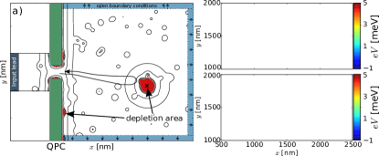
We consider a 2DEG system with a local constriction formed by the QPC [Fig. 1]. The electrons are fed from the input lead at left of the QPC. Behind the QPC the electrons propagate freely, with open boundary conditions denoted by arrows at the blue edge of Fig. 1(a). We consider the scattering of the Fermi level electrons solving the effective-mass Schrödinger equation (atomic units are used)
| (1) |
where is the two-dimensional scattering wave function with density , and is GaAs electron effective mass. In Eq. (1), contains contributions of all possible sources of electrostatic potentials considered in this paper. We assume meV which corresponds to 2DEG density of /cm2. is the QPC electrostatic potential modeled with Davies formula Davies1995 for a finite rectangular gate (green rectangles on Fig. 1(a))
where , with , , and being the left, right, bottom and top position of the gate edges, (see Fig. 1(a)). We choose the distance between 2DEG and gates to be nm. In the above formula is the gate potential. For the applied parameters, the Fermi energy meV corresponds to the first conductance plateau of the QPC. is the electrostatic potential of the charged tip, for which we use the Lorentzian approximation,
| (2) |
The Lorentzian form of the tip potential arises due to screening by the electron gas inside the heterostructure kolasinskiDFT2013 ; szafranDFT2011 ; Steinacher2015 . The width of the tip is of order of the tip - 2DEG distance and fixed at nm. The maximum potential change induced by the tip in the 2DEG is taken to be 30meV (except otherwise stated) corresponding to a depletion area of radius . This simple form of tip potential corresponds to the case of linear screening by the 2DEG electrons kolasinskiDFT2013 ; szafranDFT2011 , while the more complicated case with 2DEG depletion (i.e. when ) would require self consistent numerical calculations. Finally, the last contribution to the potential, arises from the disorder in the donor layer and it is assumed to be a superposition of uniformly distributed Gaussian functions
where is the number of impurities, is the potential amplitude generated from a uniform random distribution , is the center of the i-th Gaussian randomly distributed in the device and is the width of the Gaussians. We use nm and and for hard impurities, and nm and , for smooth impurities (see Fig. 1(b,c)).
We use the finite difference discretization of Eq. (1) and wave function matching (WFM) – described in the Appendix – in order to include the effect of the leads into the Hamiltonian and calculate the scattering amplitudes Zwierzycki2008 ; AndoWFM1991 ; Khomaykov2005 . The conductance of the system is then calculated from the Landauer formula
| (3) |
with being the Fermi-Dirac distribution, is the total transmission summed over all incoming modes in the input lead and is the conductance quantum.
III Results
III.1 Effect of disorder on the SGM maps
In Figure 2(a) we show the scattering electron density for the smooth disorder at =0K with depicted in Fig. 2(b). A branched flow is formed far from the QPC with well visible fringes Jura2007 . Near the QPC characteristic circular fringes Kolasinski2014Slit appear due to the standing wave between the QPC and the tip [see the backscattered trajectory in Fig. 1(a)]. Smooth defects lead to small-angle scattering and the branched flow remains straight over large distances. This kind of flow is found in the high mobility samples Jura2007 .

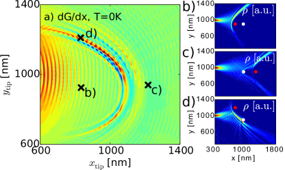
Figure 2(c) shows the scattering electron density for the case of hard impurities. The potential centers (white dots) are superimposed on the electron density image in order to show the relation between location of branches and impurity distribution within the sample. From this image one notices that the two main branches are formed along the lines with a lower impurity density (one of those branches is denoted by the black arrow in Fig. 2(d)). Not every impurity splits the electron flow in branches and the current passes across some of them.
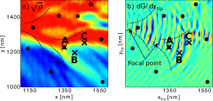
Aside from the two dominating branches in Fig. 2(c) one can see a number of characteristic funnel shaped fringe patterns denoted by the squares. Those patterns accompany the splitting of the electron density in two branches by a hard impurity in the branch. This process is schematically presented in Fig. 4(a) and can be also noted in the Fig. 3(a). Due to the finite size of the obstacle, the electron has to flow around, which leads to the funnel-shaped local widening of the branch near the impurity. In the presence of the SGM tip the electron waves can be backscattered within the funnel area (see Fig. 4(b) and (c)), which results in the characteristic circular fringes visible in Fig.3(b). At some point when the tip depletion area does not block both parts of the split branches, backscattering is reduced and circular fringes disappear from the SGM images. The funnel-shaped fringe patterns are also visible in the experimental images e.g. see in Fig. 2(b) of Refs. Paradiso2010 and Topinka2001 . Let us note that by analyzing the size of the circular fringes one may roughly estimate the depletion radius induced by the SGM tip, as the distance between the funnel focal point and the last fringe in the funnel i.e. the distance between tip location inducing the flow depicted in Figs. 4(b) and 4(d) (or points A and C in Fig. 3). From Fig. 3(b) we get an approximated value of depletion radius nm. This value of the order of the one obtained from condition , which is
| (4) |
III.2 Thermal stability of the fringes
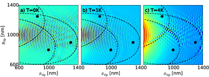
One of the most unexpected feature of the branched flow in the disordered samples is the stability of the interference fringes against thermal broadening which allows for observation of the fringes at several microns from the QPC at K, when the thermal length is only nm Topinka2000 ; Topinka2001 ; Jura2007 . In Figs. 5(a-c) we show the simulated SGM maps for a system with hard impurities at 0, 1, 4K.
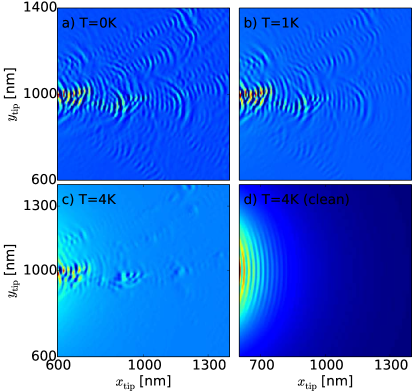
Comparing both Figs. 5(c) and (d) one can see that the persistence of the interference fringes at high temperatures at large distances is directly caused by the disorder within the sample Topinka2000 ; Topinka2001 . Additionally, a few other features can be found in the SGM images: i) interference fringes are perpendicular to the flow direction, ii) at some fringes disappear for a short distance to reappear further, iii) in general the fringe period is not uniform.
For the current flowing in branches the transport across the 2D system can be reduced to the 1D scattering system provided that the current leakage from the branch and the branch splittings are neglected. We found that the observed features of the branches can be explained within a model in which the electron branch is treated as a one dimensional electron channel. The perpendicular orientation of the fringes inside the branch is directly implied.
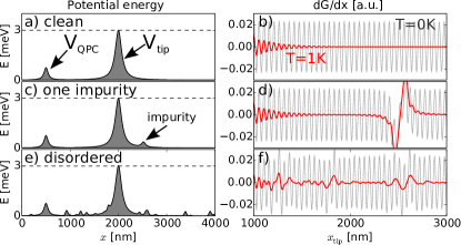
In Fig. 6(a) we show a 1D representation of a “clean” branch. An electron with kinetic energy meV is incoming from the left reservoir and scatters on the QPC and SGM tip potentials inside the channel. We set . The calculated SGM signal is presented in Fig. 6(b) for = 0 and 1 K. For K the interference fringes disappear as functions of tip position along the branch, which results from the finite width of the transport window near the Fermi level. The simulation for a single impurity within the channel [Fig. 6(c)] shows that the interference fringes reappear around the impurity [Fig. 6(d)]. This is possible when the distance between SGM tip and the impurity becomes smaller than the thermal length Jura2007 . The measured current is then sensitive to the interference which takes place far from the QPC, thus the presence of fringes in the SGM images at large distances is an evidence of nearby impurities. In Fig. 6(e-f) we show that for a disordered channel the fringes remain visible at large tip distances for K, which results from the multiple scattering between tip and nearby impurities. This effect is more dramatic in case of 2D scattering, where for 4K in Fig. 5(c) the amplitude of the fringes at some points is reduced almost to zero. One may note that at some points temperature does change the period of the fringes around the impurities in Fig. 6(f). The non-uniformity of the fringe spacing at finite temperature was experimentally observed for instance in Fig. 4 of Ref. Kozikov2015 and in Fig. 7 of Ref. Kozikov2013 .
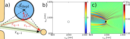
III.3 A single hard scatterer in a high mobility sample
Another interesting and previously unexplored interference scenario takes place in high mobility samples when a small number of hard impurities is present. In Fig. 7(a-c) we show SGM images for a single hard impurity within the device (with position marked by the black dot) for temperatures , 1K, and 4K. The characteristic quasi-elliptic fringes visible in the SGM images can be explained as result of the interference between electron waves following two different paths between the QPC and the impurity: (i) a direct path of length and (ii) a path of length induced by the reflection on the depleted area below the tip (see Fig. 8(a)). When the length difference is an integer multiple of the Fermi wavelength, the interference is constructive at the impurity location, resulting in a stronger backscattering and a lower conductance. The resulting interference fringes can be approximated as
| (5) |
The map calculated from Eq. (5) is presented in Fig. 8(b) and it can be compared with Fig. 8(c), where we show the SGM image calculated for a point-like tip (nm and such that nm). The white dashed lines in Fig. 8(b) and (c) represent the isolines for , i.e. the position of the tip leading to the first destructive interference between the paths marked in Fig. 8(a).
In Figs. 9(c-d) we show the scattering probability densities that are at the origin of subsequent interference fringes visible in SGM images in Fig. 9(a) or in Fig. 7(a). The circular fringes visible inside the ellipse – see Fig. 9(b) – are characteristic of a clean impurity-free sample and appear for the impurity hidden by the tip depletion area [as in Fig. 5(d)]. On the other hand in Fig. 9(c) the tip is located in the shadow of the impurity which results in strongly suppressed fringes, since very small electron flow arrives to the tip and thus the conductance map weakly depends on the tip position. In other tip positions [as in Fig. 9(d)] the process involves both the impurity and the tip [cf. Fig. 8(a)] producing the elliptic fringes.
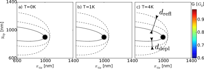
From Fig. 7(c) one can see that the elliptic pattern is thermally more stable than the circular fringes which decay rapidly with the distance to the QPC. The most stable elliptic fringe is the one for which the length difference between two paths in Fig. 8(a) is equal to the half the Fermi wavelength ( nm) – which is much shorter than the thermal length.
In order to explain the exact position of the first elliptic fringe one needs to account for the finite size of the depletion area and the electron incidence angle to the depletion area (see Fig. 8(a)). Since the kinetic energy related to the electron motion in the direction normal to the tip equipotential lines is , the reflection point is located at a distance from the tip given by . From this condition one derives the reflection radius
| (6) |
which equals the depletion radius (4) for the normal incidence , but is much larger for higher incidence angles. In Fig. 7(a-c) three lines have been drawn on the SGM images: (i) solid line is an ellipse corresponding to the first interference fringe for a point-like tip potential and denotes the first interference fringe (same as white dashed lines in Fig. 8(b-c)); (ii) The central ellipse corresponds to the smallest ellipse simply enlarged by in the normal direction; and (iii) The largest contour corresponds to the smallest ellipse but enlarged by from Eq. (6) in the normal direction. This contour is no longer an ellipse and we refer to this kind of curve by quasi-elliptic/ellipse (QE) in the following. In order to fit this model to the SGM image we have set nm in Eq. (6) which is about the nominal value of 80nm. We have to move slightly the impurity location by 20 nm to the left which is of the order of the impurity radius. The idea of the incidence-angle-dependent penetration depth was employed in a recent work of Ref. Steinacher2016 in which the authors analyzed small-angle scattering trajectories induced by potential barriers lower than the Fermi energy.
Figure 10(a-c) show SGM images for three hard impurities in the system with set of QE fringes. The dashed lines show QEs obtained from Eq. (6) with nm, which agree with the value used in the simulation. Note that for a few hard impurities, the SGM images resolve the QE fringes resulting from separate interference scenarios.
III.4 Experimental maps for hard scatterers
For the experiment we use the same series of samples as in Refs. Brun2014 ; Brun2016 for which the interference fringes between the QPC and the tip – independently of the hard scatterers – were reported previously at low temperature. The presence of hard scatterers can be more easily identified in SGM images recorded at a higher temperature, for which the "clean" interference fringes disappear. In this section, we illustrate the effects of single hard scatterers in a high mobility sample by discussing a SGM experiment performed at 4.2 K. The QPC is defined in a 2DEG located 105 nm below the surface of a GaAs/AlGaAs heterostructure. The 2DEG has a cm-2 electron density and a cm2V-1s-1 electron mobility Brun2014 ; Brun2016 . The QPC is defined by a Ti/Au split gate whose rectangular gap is 350 nm wide and 200 nm long. The device is mounted in a cryogenic scanning probe microscope and cooled down to a temperature of 4.2 K. The tip of the SGM microscope is a commercial platinum-coated AFM tip fixed with silver epoxy to a tuning fork which is used as the force sensor for topographic imaging. In SGM mode, the tip is scanned above the 2DEG with a constant tip voltage of V and a tip-to-surface distance of 35 nm. The QPC gate voltage is kept fixed at V in order to have the QPC conductance equal to one conductance quantum when the tip is far from the QPC. To enhance the sensitivity of the measurement to small tip-induced effects, a small ac voltage modulation is applied to the tip and the demodulated current response gives a transconductance signal. The conductance is measured with a 100 V ac bias voltage applied between source and drain, while the transconductance is measured with a 50 mV ac voltage applied to the tip and a 150 V dc bias voltage applied between source and drain. The current flowing through the QPC is amplified and the response to the ac excitation is measured with a lock-in technique.
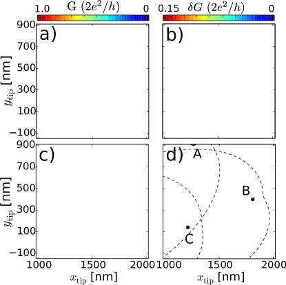
The SGM images plotted in Fig. 11(a,b) present the conductance and transconductance signals as a function of the tip position. The center of the QPC is located at coordinates as determined by SGM images recorded above the QPC and higher tip-to-surface distance (data not shown). While the conductance image simply shows the gating effect of the tip on the QPC transmission, the transconductance image shows several additional lines. The origin of these lines is attributed to the presence of hard scatterers in the 2DEG as discussed above in Sec. III.3.
In the following discussion, we assume that the lines arise from a single hard scatterer, although we are aware of the possibility that more impurities are involved. The dashed lines in Fig. 11(d) show QEs fitted using Eq. (6) in which we employ and nm for the impurities A and B. In order to fit Eq. (6) to fringes originating from impurities A and B we set position of the QPC to nm, nm and nm. Note, that the QPC position obtained from the fit is shifted with respect to the center of the QPC [ nominally (0,0)] which results from the fact that the interference result from scattering between the tip and the QPC gates – and not the QPC entrance Jura2009 – thus the QPC focal point of the QE is not located at the entrance of the QPC. At the scale of Fig. 11, the shift of from the origin is small anyway. For the impurity C we get slightly different values , nm, nm and nm. The difference in the tip potential parameters may be due to the screening of the tip by the gates ( is closer to the gates than and ). The observed number of impurities in the scanned area gives impurity density [], which can be used to roughly estimate the electron mobility inside the 2DEG with semiclassical formula , where is the mean free path. The value of is estimated from the semi-classical Broglie’s assumption of electron being a particle of diameter colliding with point like scatters uniformly distributed in the sample. The approximated expression for electron mobility reduces then to simple formula cm2V-1s-1 .
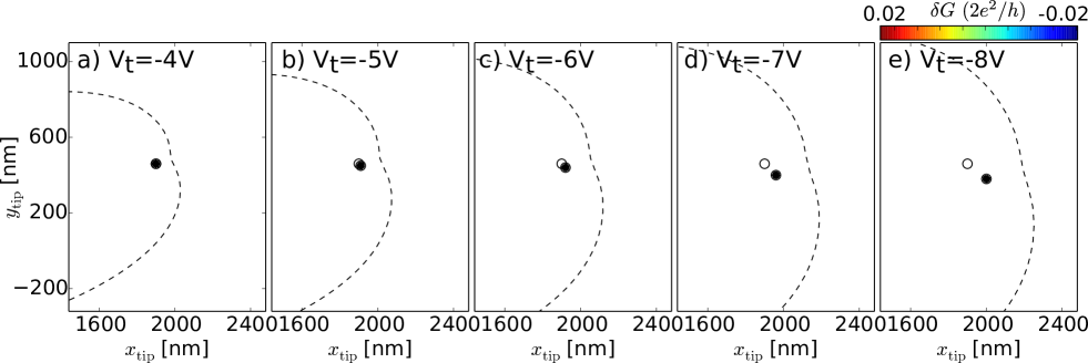
The evolution of the lines with the tip voltage is presented in Fig. 12(a-e). When the tip voltage is made more negative, the lines move to larger distances from the QPC and become wider in the transverse direction (smaller curvature). This behavior is consistent with the simulations presented in Fig. 7(c), where a larger depletion disk below the tip results in a lower eccentricity of the QE lines. The dashed lines in Figs. 12 show the results of Eq. (6) that are obtained with increasing values of nm and ratio , respectively. This non-trivial evolution of the tip-induced potential parameters (non constant and slowly varying ) reflects the complex behavior of the non-linear screening in case of partial depletion. We obtain a change of the tip radius to be about nm for a 1 V change on the tip. In order to obtain a good fit between the first QE lines and the analytical expression, we shift the positions of the impurity in Fig. 12(b-e) (filled circles) with respect to the calculated position in the first image (a) (empty circles) by about (20nm,-20nm) per image. The reason of this shift may be caused by the drift of the sample with respect to the tip position due to the long acquisition time of 2h per image.
IV Summary and Conclusions
To summarize we have discussed the role of smooth and hard impurities in the 2DEG on the SGM images. We have shown that the funnel like features that appear in conductance maps result from the splitting of the branches by hard impurities, and the position of the impurity is always shifted in the SGM images due the finite size of the depletion area. We have shown that 1D interpretation of branches can be used to explain most of the features present in the conductance maps, including their thermal stability. Additionally, we have discussed that in presence of a small number of hard impurities in high mobility sample characteristic quasi elliptic fringes can be found in the SGM images even at reasonably high temperatures . We have explained those findings in terms of interference between two paths involving both the tip and the impurity with length difference of the order of . We have provided an experimental evidence for this interference processes as well as a simple analytical formula which can be used to extract the position of the impurity and to estimate the depletion radius due to the tip.
Acknowledgments
This work was supported by National Science Centre according to decision DEC- 2015/17/N/ST3/02266, and by PL-Grid Infrastructure. The first author is supported by the scholarship of Krakow Smoluchowski Scientific Consortium from the funding for National Leading Reserch Centre by Ministry of Science and Higher Education (Poland) and by the Etiuda stipend of the National Science Centre (NCN) according to decision DEC-2015/16/T/ST3/00310. The experimental work was supported by the French Agence Nationale de la Recherche (“ITEM-exp” project) and the sample fabrication was done by U. Gennser and D. Mailly from CNRS/LPN.
Appendix
IV.1 Description of the numerical method
We start from the derivation of the scattering boundary conditions using the approach from Ref. Kirkner1990 . Let us assume that the simulated device can be approximated by tight-binding like Hamiltonian , in our case such Hamiltonian is generated from finite difference approximation of the derivatives of the differential operators in Kolasinski2016Lande . Additionally, we follow the Ref. Zwierzycki2008 and we divide the system into consecutive slices connected by coupling matrices , forming block-tridiagonal systems of linear equations for the scattering wave function inside the system
In the lead region (semi infinite lead can be located in any part of the system) the system is assumed to be homogeneous thus one may drop the indices in the matrices and write
| (7) |
which can be solved by Bloch substitution Zwierzycki2008 leading to quadratic eigenvalue equation for the transverse modes Zwierzycki2008 ; AndoWFM1991
which can be transformed to generalized eigenvalue problem (GEP) of double size
| (8) |
We solve it numerically by converting it to a standard eigenvalue problem (SEP), since in our case is invertible. If is non-invertible or ill-conditioned one may use more sophisticated methods which incorporate Singular Value Decomposition (SVD) of matrix Rungger2008 .
The eigenvalues of equation above are then grouped into incoming and outgoing modes , with each propagating mode (i.e. with ) normalized to carry the unit value of quantum flux. For more detailed description see Zwierzycki2008 .
The solution in the semi-infinite lead for the -th incoming mode can be expressed in terms of superposition transverse modes
| (9) |
where is the Bloch factor Zwierzycki2008 for the -th incoming mode and is the number of sites in the lead slice i.e. the size of the vector . Vector denotes the -th outgoing mode. For more detailed description how the transverse modes are calculated see Ref. Zwierzycki2008 . By choosing the frame of coordinates such that denotes the first slice in the considered system one may expand the wave function at this slice in terms of transverse modes
| (10) |
note that is now a part of discretized system. By projecting on Eq. (10), we get
with , which can be written in terms of matrices
with , , and . Additionally, by forcing the derivative of the wave function to be continuous at the device boundary we obtain second condition
Then by substituting the vector to the equation above we get
Let us now simplify the expression above, by starting from the first term in the sum on the right side
Where columns of matrix are constructed from transverse modes and . Analogically for the second term, we obtain
Thus we get
| (11) |
The expression above can be further simplified by noticing that , hence the matrix
The matrix is the Bloch matrix. The final formula for Eq. (11) is then
By inserting this to the Hamiltonian (7) for one removes the dependence of the slice from the linear system which gives
We note that
hence the right side can be written in a more compact form
To summarize the system of linear equation for the case of two terminal device can be written in the following way
| (12) | ||||
| (13) | ||||
| (14) |
where is the self energy calculated for left/right lead. Note, that in order to obtain open boundary conditions we use the approach from the Quantum Transmitting Boundary Method (QTBM) introduced in Ref. Kirkner1990 , but at the end we finish with the Wave Function Matching (WFM) equations Zwierzycki2008 , which shows that both methods are algebraically equivalent.
After solution of the scattering problem for a given -th incoming mode one may calculate transmission amplitudes from
| (15) |
and reflection amplitudes as
| (16) |
with and being the outgoing modes matrices for input and output lead, respectively.
References
- (1) M. A. Eriksson, R. G. Beck, M. Topinka, J. A. Katine, R. M. Westervelt, K. L. Campman, and A. C. Gossard, Applied Physics Letters 69, 671 (1996)
- (2) H. Sellier, B. Hackens, M. G. Pala, F. Martins, S. Baltazar, X. Wallart, L. Desplanque, V. Bayot, and S. Huant, Semicond. Sci. Technol. 26, 064008 (2011)
- (3) D. K. Ferry, A. M. Burke, R. Akis, R. Brunner, T. E. Day, R. Meisels, F. Kuchar, J. P. Bird, and B. R. Bennett, Sem. Sci. Tech. 26, 043001 (2011)
- (4) B. Brun, F. Martins, S. Faniel, B. Hackens, G. Bachelier, A. Cavanna, C. Ulysse, A. Ouerghi, U. Gennser, D. Mailly, S. Huant, V. Bayot, M. Sanquer, and H. Sellier, Nat Commun 5 (2014), article
- (5) B. J. van Wees, H. van Houten, C. W. J. Beenakker, J. G. Williamson, L. P. Kouwenhoven, D. van der Marel, and C. T. Foxon, Phys. Rev. Lett. 60, 848 (Feb 1988)
- (6) M. A. Topinka, B. J. LeRoy, S. E. J. Shaw, E. J. Heller, R. M. Westervelt, K. D. Maranowski, and A. C. Gossard, Science 289, 2323 (2000)
- (7) M. A. Topinka, B. J. LeRoy, R. M. Westervelt, S. E. J. Shaw, R. Fleischmann, E. J. Heller, K. D. Maranowski, and A. C. Gossard, Nature 410, 183 (2001)
- (8) A. A. Kozikov, R. Steinacher, C. Rössler, T. Ihn, K. Ensslin, C. Reichl, and W. Wegscheider, Nano Lett. 15, 7994 (2015)
- (9) M. P. Jura, M. A. Topinka, L. Urban, A. Yazdani, H. Shtrikman, L. N. Pfeiffer, K. W. West, and D. Goldhaber-Gordon, Nat Phys 3, 841 (2007), ISSN 1745-2473
- (10) M. P. Jura, M. A. Topinka, M. Grobis, L. N. Pfeiffer, K. W. West, and D. Goldhaber-Gordon, Phys. Rev. B 80, 041303 (2009)
- (11) M. Kumar, S. Lahon, P. K. Jha, and M. Mohan, Superlattices Microstruct. 57, 11 (2013)
- (12) E. J. Heller and S. Shaw, Int. J. Mod. Phys. B 17, 3977 (2003)
- (13) B. Liu and E. J. Heller, Phys. Rev. Lett. 111, 236804 (Dec 2013)
- (14) B. Liu, Journal of Physics: Conference Series 626, 012037 (2015)
- (15) K. Kolasiński, B. Szafran, and M. P. Nowak, Phys. Rev. B 90, 165303 (2014)
- (16) J. H. Davies, I. A. Larkin, and E. V. Sukhorukov, J. Appl. Phys 77, 4504 (1995)
- (17) K. Kolasiński and B. Szafran, Phys. Rev. B 88, 165306 (2013)
- (18) B. Szafran, Phys. Rev. B 84, 075336 (2011)
- (19) R. Steinacher, A. A. Kozikov, C. Rössler, C. Reichl, W. Wegscheider, T. Ihn, and K. Ensslin, New J. Phys. 17, 043043 (2015)
- (20) M. Zwierzycki, P. A. Khomyakov, A. A. Starikov, K. Xia, M. Talanana, P. X. Xu, V. M. Karpan, I. Marushchenko, I. Turek, G. E. W. Bauer, G. Brocks, and P. J. Kelly, Phys. Stat. Sol. 245, 623 (2008)
- (21) T. Ando, Phys. Rev. B 44, 8017 (1991)
- (22) P. A. Khomyakov, G. Brocks, V. Karpan, M. Zwierzycki, and P. J. Kelly, Phys. Rev. B 72, 035450 (2005)
- (23) N. Paradiso, S. Heun, S. Roddaro, L. Pfeiffer, K. West, L. Sorba, G. Biasiol, and F. Beltram, Physica E 42, 1038 (2010), 18th International Conference on Electron Properties of Two-Dimensional Systems
- (24) A. A. Kozikov, C. Rössler, T. Ihn, K. Ensslin, C. Reichl, and W. Wegscheider, New Journal of Physics 15, 013056 (2013)
- (25) R. Steinacher, A. A. Kozikov, C. Rössler, C. Reichl, W. Wegscheider, K. Ensslin, and T. Ihn, Phys. Rev. B 93, 085303 (2016)
- (26) B. Brun, F. Martins, S. Faniel, B. Hackens, A. Cavanna, C. Ulysse, A. Ouerghi, U. Gennser, D. Mailly, P. Simon, S. Huant, V. Bayot, M. Sanquer, and H. Sellier, Phys. Rev. Lett(2016), (to be published)
- (27) C. S. Lent and D. J. Kirkner, J. Appl. Phys. 67, 6353 (1990)
- (28) K. Kolasiński, A. Mreńca-Kolasińska, and B. Szafran, Phys. Rev. B 93, 035304 (2016)
- (29) I. Rungger and S. Sanvito, Phys. Rev. B 78, 035 (2008)