Impact of ex-situ rapid thermal annealing on the magneto-optical properties and the oscillator strength of In(Ga)As quantum dots
Abstract
We discuss the influence of a rapid thermal annealing step on the magneto-optical emission properties of In(Ga)As/GaAs quantum dots. We map out a strong influence of the growth- and anneling parameters on the quantum excitons’ effective Landé g-factors and in particular on their diamagnetic coefficients, which we directly correlate with the modification of the emitters shape and material composition. In addition, we study the excitons’ spontaneous emission lifetime as a function of the annealing temperature and the dot height, and observe a strong increase of the emission rate with the quantum dot volume. The corresponding increase in oscillator strenth yields fully consistent results with the analysis of the diamagenic behavior. In particular, we demonstrate that a rapid thermal annealing step of 850∘ C can be employed to increase the oscillator strength of as-grown InAs/GaAs QDs by more than a factor of .
I Introduction
Tremendous progress has been achieved the last years in understanding and exploiting the electronic as well as the photonic characteristics of semiconductor quantum dots (QDs), resulting in remarkable achievements such as the observation of triggered single photon emissionMichler et al. (2000); Santori et al. (2001); Moreau et al. (2001), generation of highly indistinguishableSantori et al. (2002); He et al. (2013) and entangledAkopian et al. (2006) photon pairs as well as reaching the strong coupling regime of a single solid state quantum emitter and the localized field of a cavity modeReithmaier et al. (2004); Yoshie et al. (2004); Peter et al. (2005). The QD’s oscillator strength (OS) is a dimensionless parameter describing the strength of the coupling of a transition from an excited to the ground state of a quantum emitter to the surrounding light field and is therefore a crucial factor in any kind of cavity quantumelectrodynamics (cQED) experiment. A larger OS leads to a stronger light matter interaction (light matter coupling constant ) which is, e.g. crucial to reach the strong coupling regime where a coherent exchange of light and matter is possible. In the limit of weak confinement of an exciton in a QD, the OS is associated to the QD’s size. Thus, morphologically large QDs in the III/V semiconductor system such as low strain InGaAs QDs ( up to 50)Reithmaier et al. (2004) and natural GaAs islands ()Peter et al. (2005) have been identified to particularly promote strong coupling conditions. As these QDs evolve just at the layer-to-island transition of the Stranski-Kranstanov growth mode, or form as natural islands driven by surface migration, routinely reproducing and engineering QDs with a high OS is very difficult.
Several groups have shown that rapid thermal annealing (RTA) of InAs QDs is a useful technique to take influence on the emission properties after the growing process. For example, RTA allows for tailoring the QD size, the indium composition and with that the emission energy as well as the linewidth of the quantum dot ensembleKosogov et al. (1996); Leon et al. (1996); Fafard and Allen (1999); Nishi et al. (1999); Hsu et al. (2000). Furthermore it is possible to adjust the dephasing time of QD excitonsLangbein et al. (2004). Recently, it also has been indicated that post growth, rapid thermal annealing of InAs QDs can also be exploited to significantly enhance the oscillator strength of QDsLoo et al. (2010). While these results are very promising, a thorough investigation of the effect of rapid thermal annealing on the intrinsic excitonic properties is still elusive. Here, in a systematic analysis we demonstrate the influence of a rapid thermal annealing (RTA) process on the QD properties via magnetic field dependent micro-photoluminescence ( PL) and time resolved spectroscopy. We show an increase of the mean lateral expansion of the exciton wavefunction in InAs/GaAs QDs by about 70% and more than a doubling of the OS under appropriate growth and annealing conditions. Furthermore, we demonstrate that measuring the diamagnetic response of a QD exciton is a viable tool to directly assess the emitter’s oscillator strength as it yields reliable and consistent results on the single emitter scale.
II Theory
To describe a QD in a magnetic field on a basic level, we consider the exciton energy without magnetic field, the Zeeman interaction between electrons and holes and the diamagnetic shift energy which is induced by the external magnetic field. The total energy of the system in a magnetic field in Faraday configuration () is then given by:
| (1) |
with the Bohr magneton and an effective excitonic Landé-factor in the Zeeman-term. The diamagnetic coefficient is defined byBabinski et al. (2006):
| (2) |
Hereby gives the mean quadratic expansion of the wave function of the carriers.
The dimensionless oscillator strength describes the coupling strength between the light field and the transition from an excited to the ground state of the emitter. It indicates the absorption and recombination probability in bulk material and depends primarily on the overlap of the wave functions of the electron and the hole. can be correlated with the radiative decay rate viaHours et al. (2005):
| (3) |
where is material’s the refractive index. For QDs which are larger than the excitonic Bohr radius (this is the so-called limit of weak confinement), can be approximated byStobbe et al. (2010):
| (4) |
Here is the Kane-energyKane (1957) and the expansion of the center-of-mass wave function in the plane perpendicular to the growth direction of the QD.
III Sample design and experimental methods
III.1 Sample preparation
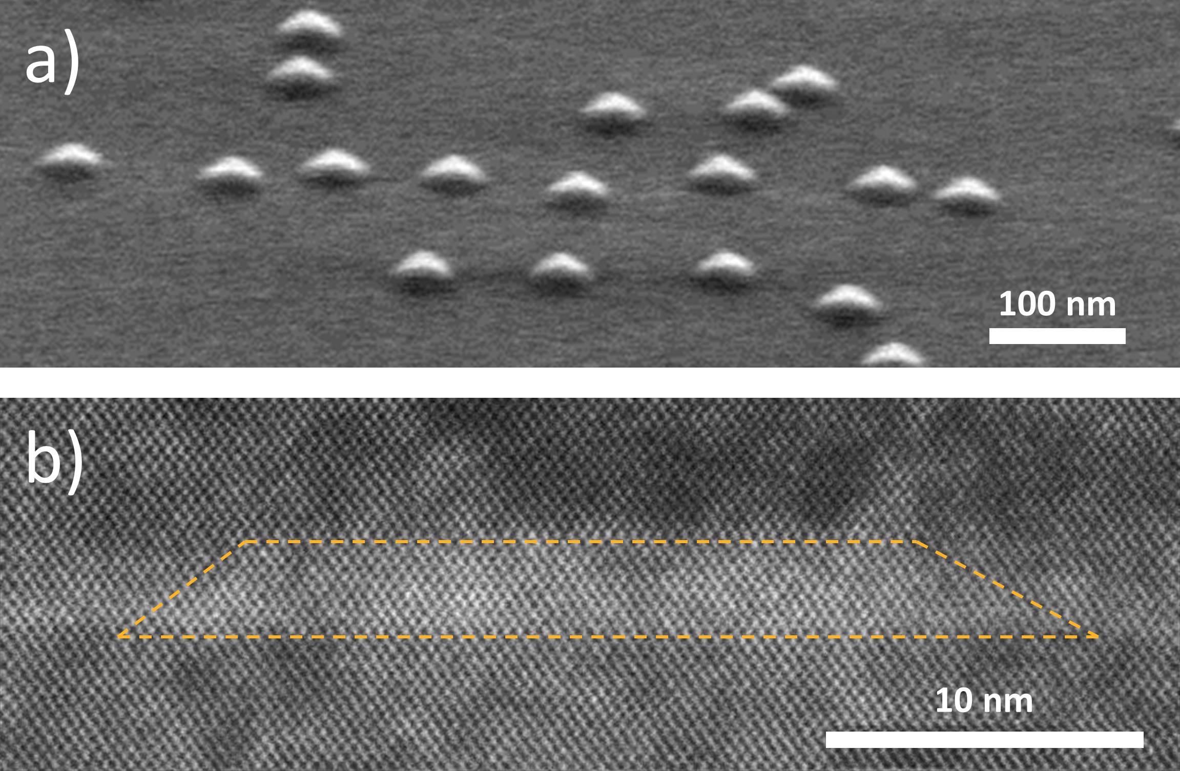
The QDs under consideration were grown via molecular beam epitaxy (MBE) and treated by the partial capping and annealing (PCA) technique. The InAs-QDs deposited on a GaAs buffer layer were overgrown by a GaAs cap layer and were then in-situ annealed for one minute at a nominal substrate temperature of 560∘ C. The PCA process leads to an enhanced interdifusion of the Ga- and In-atoms and flushes away the uncovered QD tipGarcia et al. (1997). The QD height and hence the emission energy hereby strongly depend on the cap thickness. After the in-situ annealing process the crystal growth was completed by a 100 nm thick GaAs cap to circumvent nonradiative surface recombination. The emission frequency of the QDs can additionally be tuned by an ex-site rapid thermal annealing (RTA) step. Thereby the samples were heated up to temperatures in the range of 750∘ C to 850∘ C for 5 minutes. Thus the interdiffusion process is boosted again and the further mixing of the atoms leads to an increase in the QD volume. In addition a blue shift of the emission takes place due to the reduction of the In content in the QDLeon et al. (1996); Fafard and Allen (1999); Hsu et al. (2000). For a detailed analysis of the influence of the annealing process on the OS we have grown three samples with a varying cap thickness from 2 nm to 4 nm. Each specimen was cleaved into four pieces, and three of these pieces were treated via RTA at 750∘ C, 800∘ C and 850∘ C. For the fourth piece, the annealing step was omitted and the sample served as a reference. Fig. 1 shows a scanning electron microscope (SEM) image of the surface QDs prior to the capping (a) and a scanning transmission electron microscope (STEM) image of a QD after the growth of the full structure has been accomplished (b). The thickness of the partial cap was chosen to in this particular sample. While the surface QDs exhibit the typical pyramidal shape, the top side of the overgrown QD is significantly flattened and QD height decreased down to the thickness of the capping layer.
III.2 Experimental methods
Magneto-optical studies were performed at a temperature of 5 K using a high resolution PL setup. The magnet cryostat provides magnetic flux densities up to 5 T in Faraday configuration. The samples were excited with a Ti:Sapphire laser tuned to 780 nm which can be operated in cw- as well as in pulsed-mode with a repetition rate of 82 MHz. The emitted photons were collected by a 50x microscope objective (), dispersed by a grating with 1200 lines/mm and detected with a LN2 cooled Si-CCD. The magneto-optical measurements were performed in cw-mode. To investigate the Zeeman-splitting, a quarter wave plate was mounted in addition to a linear polarizer. Adjusting the quarter wave plate accurately in an angle of with respect to linear polarizer we can extract the circular polarized part of the QD emission.
The samples were also investigated under pulsed excitation in order to measure the lifetime of the QDs. The emission signal of the quantum dot ensemble was filtered by the monochromator and then focused on a fiber-coupled avalanche photo diode (APD) with a temporal resolution of ps.
IV Experimental results
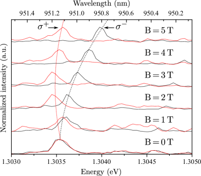
Figure 2 shows a typical emission spectrum of a QD at different magnetic fields. The investigated sample was the reference sample with a cap thickness of 3 nm. The intensity was normalized for each spectrum. Since the typical QD fine structure splitting (FSS) is on the order of 10 eV for these QDs and the resolution of our setup is about 35 eV no notable splitting was detected (without performing more sophisticated measurements). However, one clearly sees the influence of the magnetic field (cf. equation 1) on the QD emission energy. The Zeeman splitting between the right ()- and left ()-circular polarized photons increases linearly with the magnetic field and the diamagnetic shift superimposes the split doubled.
IV.1 Zeeman splitting and Landé g-factor
In order to study the evolution of the Zeeman splitting and the effective Landé g-factors of the QDs in greater detail, we plot the energetic gap between the and the emission, which is defined as , as a function of the magnetic field. The result for each sample is depicted in fig. 3 a)-c). Up to 9 different QDs per sample were investigated and the resulting mean value was plotted. Spectra were taken every 0.5 T up to a magnetic flux density of 5 T. We assume that the emission is completely circular polarized for Bayer et al. (2002).
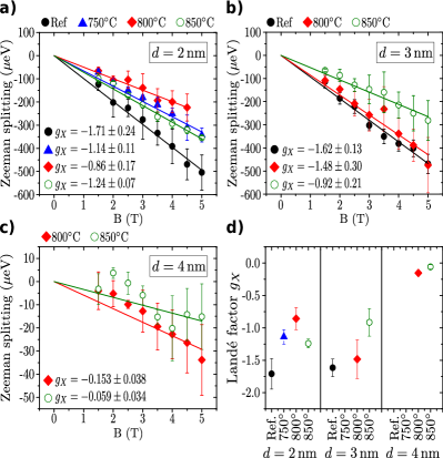
For each cap thickness a decrease of the Zeeman splitting and accordingly the g-factors is observable for increasing annealing temperatures. According to equation 1 the effective g-factor can be obtained by a linear fit. The absolute g-value of the QDs of the sample with drops from for the reference sample to at a temperature of 800∘ C (cf. fig. 3 a)). We attribute this effect to the interdiffusion of the Ga- with the In-atoms which leads to a lateral expansion of the QDs. According to Bayer et al.Bayer et al. (1995) and Kotlyar et al.Kotlyar et al. (2001) should be proportional to ( is the QD diameter). This effect is caused by spin-orbit interactions which increase with decreasing QD size due to the uncertainty relation. Furthermore we would like to note that also the composition in the QD significantly modifies both with the annealing temperature and the dot size, and thermal annealing additionally leads to a strain variation in the QD which results in a reduction of the absolute -valueNakaoka et al. (2005). This is consistently observed in fig. 3d, where we depict all obtained g-factors for varying cap thicknesses and annealing temperatures. The highest absolute -value is measured for the reference sample with with and the lowest for the sample with a 4 nm cap annealed at 850∘ C with . We note that the emission band of the sample with a cap thickness of 4 nm was outside of the detection window of our Si-CCD camera (both for the reference sample and the sample piece that was annealed at 750∘ C).
IV.2 Diamagnetic coefficient
Next, we study the diamagentic behavior of the emitters as a function of the annealing conditions. We plot the magnitude of the diamagnetic shift (which can be obtained via the energy mean value of the and emission lines) against the square of the magnetic field. Then a linear fit is applied to the data to extract the diamagnetic coefficient . The results are shown in fig. 4.
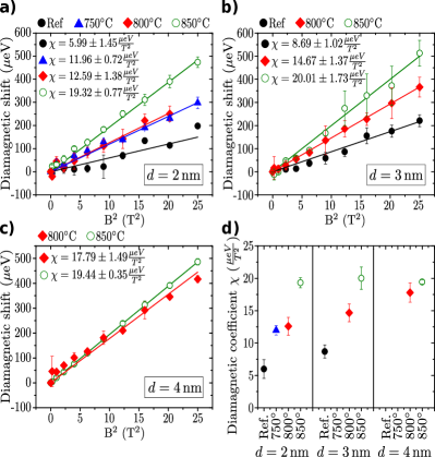
For all three chosen cap thicknesses we observe a distinct increase of the diamagnetic coefficient for higher ex-situ annealing temperatures. In addition, an increasing for the same temperatures and higher cap thicknesses can be noted (for ). It is reasonable to assume that thicker caps and higher temperatures lead to an increase of the lateral expansion of the QDs since is proportional to the expansion of the wave functions according to equation 2. With equation 4 and the approximation of Reitzenstein et al. (2009) we can estimate the mean lateral expansion of the wavefunction and can calculate the OS (cf. equation 2):
| (5) |
The determined values for will be discussed later in section IV.4 and are plotted as black squares in fig. 6. It should be noted that L is not equivalent to the physical expansion of our quantum dots as seen in the TEM image in figure 1. The determined L value (8.1 nm) and the average diameter of the quantum dots taken from TEM analysis (25.8 nm) deviate significantly. In order to explain the difference we performed six-band-kp model based calculations of the wave functions, using the software Nextnano Trellakis et al. (2006). For this, we used geometric parameters taken from TEM analyis. The resulting mean diameters of the wave functions are 9.8 nm for the electron wave function and 12.4 nm for the hole wave function . Therefore, the significant deviation between L and D are not in contradiction.
IV.3 Time resolved spectroscopy
According to equation 3 the OS is directly related to the radiative decay time of the quantum emitter. Therefore, measuring the lifetime of the QDs is another way to study the influence of ex-situ RTA on the OS. Fig 5 a) exemplarily shows the QD ensemble emission of the reference sample with . In this range we performed lifetime measurements by measuring gradually the monochromator filtered emission wavelength (spectral range 0.2 nm) over the whole QD emission spectrum. The lifetimes aquired at the spectral positions used for determination of the diamagnetic shift and the Zeeman splitting are plotted in fig. 5 b).
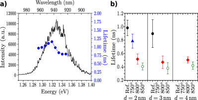
One cleary sees that a higher annealing temperature results in an enhancement of the spontaneous emission decay rate. Since is proportional to we note that the annealing procedure is a viable tool to increase the QD’s oscillator strenght, as we detail in the next section.
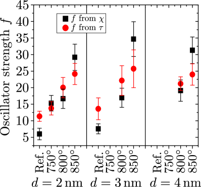
IV.4 Oscillator strength
| Annealing temperature | In content | (nm) | (from ) | (from ) | ||||
| 2 nm | not annealed | |||||||
| 750∘ C | ||||||||
| 800∘ C | ||||||||
| 850∘ C | ||||||||
| 3 nm | not annealed | |||||||
| 800∘ C | ||||||||
| 850∘ C | ||||||||
| 4 nm | 800∘ C | |||||||
| 850∘ C |
We now give a more detailed analysis of the data. Based on equation 5 and 3 we can calculate the OS from the experimental data. This calculation requires knowledge of the In content in the QDs. The In content was estimated in the following way: First, Nextnano simulations were carried out for the as-grown QDs, by adjusting the In content of the simulated QD in a way that the calculated transition energies matched the experimentally measured PL energies. The geometric parameters of the QDs were taken from the TEM analysis. The STEM analysis shows that the actual QD height (2.9 nm) is in very good agreement with the nominal height of the capping layer (3 nm). Therefore, 2 nm, 2.9 nm and 4 nm were used as QD heights for the respective samples. A QD width of 26 nm was used for all three nominal capping layer heights since the QD width is not expected to vary significantly between different capping procedures. In a second step we performed a boxcar type smoothing algorithm based on Fick’s law to simulate the reduction of In content during the annealing process. The results of this calculations are compiled in the third column of table 1. Finally, we use these estimations of the In content to calculate the oscillator strength for the acquired data. All other material dependent parameters were taken from literatureColdren et al. (1995); Stier et al. (1999); Vurgaftman et al. (2001).
Almost all values for derived from the diamagnetic shift as well from the lifetime measurements agree within the error bars (see fig. 6). The highest OS derived from the diamagnetic shift has been obtained for a cap thickness of and an annealing temperature of 850∘ C. The maximum OS from the lifetime measurements was calculated also for and a temperature of 850∘ C. For not annealed samples Warbuton et al.Warburton et al. (1997) indicates a OS about 10 which, indeed, is good agreement with our reference samples. Furthermore an increase of the lateral expansion of the QD wave function from of the reference sample with to for and a temperature of 850∘ C can be extracted from table 1, where we provide a full list of extracted parameters. In summary we have shown that the mean lateral expansion of the wavefunction increases by about 70% and the OS has more than doubled due to an ex-situ RTA process.
V Summary
In conclusion with have systematically investigated the influence of an ex-situ rapid thermal annealing process on InAs/GaAs PCA QDs with various cap thicknesses . We studied the emission properties of these QDs in a magnetic field and extracted the effective Landé g-factor and the diamagnetic coefficient . Both show a strong dependency on the annealing temperature as well as on the cap thickness. From these measurements we could derive the mean lateral expansion of the wavefunction and the oscillator strength of the QDs. Furthermore we compared the results to time resolved measurements to extract the oscillator strength on the QD ensemble. In these studies, we could confirm that RTA has a consistently positive effect on the oscillator strength of an InAs quantum emitter, which makes this technique highly appealing for post growth engineering dynamic emitter properties. We furthermore emphasize that both approaches, namely time resolved spectroscopy and magneto optical measurements yield values which are in very good agreement.
Acknowledgment
The authors acknowledge financial support by the State of Bavaria and the German Ministry of Education and Research (BMBF) within the project Q.com. We thank M. Lermer for sample fabrication.
Appendix A Modeling the effect of annealing
To simulate the effect of annealing we turned to a boxcar type smoothing algorithm. We started with a quantum dot having uniform In-distribution inside the boundaries of a capped pyramid. Subsequently, this proto-QD is being annealed applying -times the operation
| (6) |
with being the Indium concentration at coordinates of the numerical grid. The number refers to the number of smoothing steps. Then, for each a complete electronic structure calculation is carried out, thus accounting for the corresponding material redistribution, the resulting strain and piezoelectricity. The single particle states are calculated using a 3D implementation of eight-band-kp theory and the electron-hole pair lifetime is obtained within the dipole approximation.
Appendix B Effect of annealing on the optical properties of the samples
Ensemble photoluminescence spectra (excitation spot diameter 100 m) recorded at 10 K for the sample with a 2 nm high partial cap are plotted in Fig. 7. The spectra correspond to the four selected annealing conditions, which are also addressed in the main text. From these spectra, the intermixing induced emission blueshift and the narrowing in the ensembles’ inhomogeneous broadening becomes obvious, in agreement with previous reports.Kosogov et al. (1996); Fafard and Allen (1999); Nishi et al. (1999); Hsu et al. (2000); Leon et al. (1996).
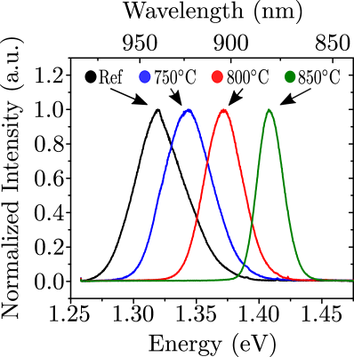
| Annealing temperature | (eV) | (meV) | FWHM (meV) |
|---|---|---|---|
| not annealed | 1.321 | — | 47.9 |
| 750∘ C | 1.343 | 22.3 | 45.0 |
| 800∘ C | 1.372 | 50.7 | 35.7 |
| 850∘ C | 1.409 | 87.9 | 24.1 |
References
- Michler et al. (2000) P. Michler, A. Kiraz, C. Becher, W. V. Schoenfeld, P. M. Petroff, L. Zhang, E. Hu, and A. Imamoglu, Science 290, 2282 (2000).
- Santori et al. (2001) C. Santori, M. Pelton, G. Solomon, Y. Dale, and Y. Yamamoto, Phys. Rev. Lett. 86, 1502 (2001).
- Moreau et al. (2001) E. Moreau, I. Robert, J. M. Gérard, I. Abram, L. Manin, and V. Thierry-Mieg, Applied Physics Letters 79, 2865 (2001).
- Santori et al. (2002) C. Santori, D. Fattal, J. Vuckovic, G. S. Solomon, and Y. Yamamoto, Nature 419, 594 (2002).
- He et al. (2013) Y.-M. He, Y. He, Y.-J. Wei, D. Wu, M. Atature, C. Schneider, S. Hofling, M. Kamp, C.-Y. Lu, and J.-W. Pan, Nat Nano 8, 213 (2013).
- Akopian et al. (2006) N. Akopian, N. Lindner, E. Poem, Y. Berlatzky, J. Avron, D. Gershoni, B. Gerardot, and P. Petroff, Phys. Rev. Lett. 96, 130501 (2006).
- Reithmaier et al. (2004) J. P. Reithmaier, G. Sek, A. Loffler, C. Hofmann, S. Kuhn, S. Reitzenstein, L. V. Keldysh, V. D. Kulakovskii, T. L. Reinecke, and A. Forchel, Nature 432, 197 (2004).
- Yoshie et al. (2004) T. Yoshie, A. Scherer, J. Hendrickson, G. Khitrova, H. M. Gibbs, G. Rupper, C. Ell, O. B. Shchekin, and D. G. Deppe, Nature 432, 200 (2004).
- Peter et al. (2005) E. Peter, P. Senellart, D. Martrou, A. Lemaître, J. Hours, J. Gérard, and J. Bloch, Phys. Rev. Lett. 95, 067401 (2005).
- Kosogov et al. (1996) A. O. Kosogov, P. Werner, U. Gösele, N. N. Ledentsov, D. Bimberg, V. M. Ustinov, A. Y. Egorov, A. E. Zhukov, P. S. Kop’ev, N. A. Bert, and Z. I. Alferov, Applied Physics Letters 69, 3072 (1996).
- Leon et al. (1996) R. Leon, Y. Kim, C. Jagadish, M. Gal, J. Zou, and D. Cockayne, Applied physics letters 69, 1888 (1996).
- Fafard and Allen (1999) S. Fafard and C. N. Allen, Applied Physics Letters 75, 2374 (1999).
- Nishi et al. (1999) K. Nishi, H. Saito, S. Sugou, and J.-S. Lee, Applied Physics Letters 74, 1111 (1999).
- Hsu et al. (2000) T. M. Hsu, Y. S. Lan, W.-H. Chang, N. T. Yeh, and J.-I. Chyi, Applied Physics Letters 76, 691 (2000).
- Langbein et al. (2004) W. Langbein, P. Borri, U. Woggon, V. Stavarache, D. Reuter, and A. D. Wieck, Phys. Rev. B 70, 033301 (2004).
- Loo et al. (2010) V. Loo, L. Lanco, A. Lemaître, I. Sagnes, O. Krebs, P. Voisin, and P. Senellart, Applied Physics Letters 97, 241110 (2010).
- Babinski et al. (2006) A. Babinski, G. Ortner, S. Raymond, M. Potemski, M. Bayer, W. Sheng, P. Hawrylak, Z. Wasilewski, S. Fafard, and A. Forchel, Phys. Rev. B 74, 075310 (2006).
- Hours et al. (2005) J. Hours, P. Senellart, E. Peter, A. Cavanna, and J. Bloch, Phys. Rev. B 71, 161306 (2005).
- Stobbe et al. (2010) S. Stobbe, T. Schlereth, S. Höfling, A. Forchel, J. Hvam, and P. Lodahl, Phys. Rev. B 82, 233302 (2010).
- Kane (1957) E. O. Kane, Journal of Physics and Chemistry of Solids 1, 249 (1957).
- Garcia et al. (1997) J. M. Garcia, G. Medeiros-Ribeiro, K. Schmidt, T. Ngo, J. L. Feng, A. Lorke, J. Kotthaus, and P. M. Petroff, Applied Physics Letters 71, 2014 (1997).
- Bayer et al. (2002) M. Bayer, G. Ortner, O. Stern, A. Kuther, A. Gorbunov, A. Forchel, P. Hawrylak, S. Fafard, K. Hinzer, T. Reinecke, S. Walck, J. Reithmaier, F. Klopf, and F. Schäfer, Phys. Rev. B 65, 195315 (2002).
- Bayer et al. (1995) M. Bayer, V. Timofeev, T. Gutbrod, A. Forchel, R. Steffen, and J. Oshinowo, Phys. Rev. B 52, R11623 (1995).
- Kotlyar et al. (2001) R. Kotlyar, T. Reinecke, M. Bayer, and A. Forchel, Phys. Rev. B 63, 085310 (2001).
- Nakaoka et al. (2005) T. Nakaoka, T. Saito, J. Tatebayashi, S. Hirose, T. Usuki, N. Yokoyama, and Y. Arakawa, Phys. Rev. B 71, 205301 (2005).
- Reitzenstein et al. (2009) S. Reitzenstein, S. Münch, P. Franeck, A. Rahimi-Iman, A. Löffler, S. Höfling, L. Worschech, and A. Forchel, Phys. Rev. Lett. 103, 127401 (2009).
- Trellakis et al. (2006) A. Trellakis, T. Zibold, T. Andlauer, S. Birner, R. K. Smith, R. Morschl, and P. Vogl, Journal of Computational Electronics 5, 285 (2006).
- Warburton et al. (1997) R. Warburton, C. Dürr, K. Karrai, J. Kotthaus, G. Medeiros-Ribeiro, and P. Petroff, Phys. Rev. Lett. 79, 5282 (1997).
- Coldren et al. (1995) L. Coldren, S. Corzine, and M. Mashanovitch, Diode Lasers and Photonic Integrated Circuits, Wiley Series in Microwave and Optical Engineering (Wiley, 1995).
- Stier et al. (1999) O. Stier, M. Grundmann, and D. Bimberg, Phys. Rev. B 59, 5688 (1999).
- Vurgaftman et al. (2001) I. Vurgaftman, J. R. Meyer, and L. R. Ram-Mohan, Journal of Applied Physics 89, 5815 (2001).