Influence of rhombohedral stacking order in the electrical resistance of bulk and mesoscopic graphite
Abstract
The electrical, in-plane resistance as a function of temperature of bulk and mesoscopic thin graphite flakes obtained from the same batch was investigated. Samples thicker than nm show metalliclike contribution in a temperature range that increases with the sample thickness, whereas a semiconductinglike behavior was observed for thinner samples. The temperature dependence of the in-plane resistance of all measured samples and several others from literature can be very well explained between 2 K and 1100 K assuming three contributions in parallel: a metalliclike conducting path at the interfaces between crystalline regions, composed of two semiconducting phases, i.e. Bernal and rhombohedral stacking. From the fits of we obtain a semiconducting energy gap of meV for the rhombohedral and meV for the Bernal phase. The presence of these crystalline phases was confirmed by x-ray diffraction measurements. We review similar experimental data from literature of the last 33 years and two more theoretical models used to fit .
pacs:
72.20.-i,73.20.-r,73.40.-cI Introduction
Graphite, a layered material built by weakly coupled graphene sheets, is a material being studied experimentally and theoretically for more than fifty years. Usually, the graphene layers adopt an hexagonal (2H) stacking sequence called the Bernal Bernal (1924) structure. However, another stable phase in graphite has an stacking order called rhombohedral (3R) graphite Lipson and Stokes (1942). According to early literature Lipson and Stokes (1942); Kelly (1981), high quality graphite samples can be composed of up to rhombohedral and the rest Bernal phase. Recent studies on exfoliated few-layer graphene (FLG) using Raman spectroscopy, show domains of different stacking order with of the total area displaying 3R stacking Lui et al. (2011). The domains exhibiting 3R stacking in FLG are stable after annealing to C Lui et al. (2011) and to C in bulk graphite Matuyama (1956); Freise and Kelly (1963).
Wallace calculated the band structure of graphite within tight-binding approximation with the result that graphite behaves like a semiconductor with a vanishing small energy gap Wallace (1947a, b). The existence of a finite energy gap in graphite was proposed by Mrozowsky based on the analysis of electrical resistivity and diamagnetism of polycrystalline graphite Mrozowski (1952, 1950). Recent theoretical work on 3R graphite suggests the formation of an energy gap that should become smaller increasing the number of graphene layers of the 3R phase Guinea et al. (2006); Koshino and McCann (2009); Koshino (2010). By means of angle-resolved photoemission Coletti et al. (2013) the existence of an energy gap of the order of 100 meV in trilayer 3R graphite was obtained. The study of the electrical transport properties of bulk graphite dates back to Dutta for single crystals Dutta (1953) and to Reynolds for natural and polycrystalline samples Reynolds et al. (1953). Since then, none of the large number of published studies on the transport properties of graphite considered the influence of the 3R phase, even though there is no doubt about its existence in usual graphite samples.
The presence of the 3R phase in graphite samples can have a further, drastic influence on their transport properties. Recent theoretical work predicts a topological protected flat band at the surface of 3R graphite Kopnin et al. (2011), which was recently confirmed experimentally Pierucci et al. (2015). Moreover, assuming a finite Cooper-pair coupling, this flat band might trigger high-temperature superconductivity Heikkilä et al. (2011); Heikkilä and Volovik (2011); Kopnin et al. (2013), which should exist also at the embedded interfaces between Bernal and 3R crystalline phases Kopnin and Heikkilä (2015); Muñoz et al. (2013) and/or at twisted single Bernal phases Esquinazi et al. (2014). Therefore, the presence of both stacking orders in a graphite sample can have clear competitive contributions to the conductivity of real samples.
In this work, the influence of 3R stacking on the in-plane resistance of 11 samples, bulk and mesoscopic graphite flakes, was studied. The presence of both stacking orders was confirmed by x-ray diffraction (XRD), see Section II. In Section III we show that assuming the contributions of the two crystalline stacking plus a metalliclike contribution from the interfaces in parallel, we are able to fit the temperature dependence of the resistance of all samples in a broad temperature range. From the fits we obtain an energy gap for the 3R stacking regions in our samples in agreement with results from literature Coletti et al. (2013). Furthermore, in Section IV we show that our model describes with high degree of accuracy published resistance data of macroscopic and mesoscopic samples of different thickness in a broad range of temperature, i.e. from 2 K to 1100 K Endo et al. (1983); Ohashi et al. (1997); Gutman et al. (2009), using as fitting parameters similar energy gaps. A detailed comparison of the proposed models in literature to explain the temperature dependence of the resistance of graphite Ohashi et al. (1997); Gutman et al. (2009) in a large temperature range, reveals that the proposed models do not really fit the published data, independently of the used fitting parameters.
II Experimental details and sample quality characterization
The graphite samples used for experiments were obtained from highly oriented pyrolytic graphite (HOPG) bulk material from Advanced Ceramic with a rocking curve width of and metallic impurities in the ppm range Spemann et al. (2014). Investigated mesoscopic flakes were produced on top of silicon substrates caped with a 150 nm thick insulating silicon nitride (). For this work, the flakes were produced by a rubbing method already described in previous publications Barzola-Quiquia et al. (2008). After selecting suitable samples, electron beam lithography was used to print the structures for the electrodes, which were sputtered with a bilayer of CrAu with a thickness of nm and nm, respectively. The temperature dependent resistance of the samples was measured in a commercial cryostat, within the temperature range of 2 K to 310 K. Low noise resistance measurements were performed using an AC Bridge (Linear Research LR-700), with a constant current .
| Sample | Thickness (nm) | (meV) | (meV) | (meV) | |||||
|---|---|---|---|---|---|---|---|---|---|
| GB1 | 6000 | 1.2 E-4 | 10 E-4 | 106 | 40 | 4.0 | 0.33 | 0.0018 | 0.61 |
| GF2 | 85 | 8.2 E-5 | 7.3 E-4 | 97 | 25 | 4.9 | 0.28 | 0.0028 | 1.14 |
| GF3 | 50 | 9.1 E-5 | 12.6 E-4 | 104 | 35 | 3.9 | 0.6 | 0.0012 | 0.68 |
| GF4 | 115 | 5.8 E-5 | 7.8 E-4 | 90 | 29 | 4.8 | 0.6 | 0.0075 | 0.77 |
| GF5 | 80 | 7.7 E-5 | 7.0 E-4 | 107 | 39 | 4.1 | 0.72 | 0.0016 | 0.67 |
| GF6 | 95 | 9.7 E-5 | 9.5 E-4 | 98 | 32 | 4.5 | 0.73 | 0.0011 | 0.72 |
| GF7 | 80 | 8.5 E-5 | 10 E-4 | 105 | 36 | 4.0 | 0.73 | 0.0011 | 0.69 |
| GF8 | 72 | 8.1 E-5 | 8.9 E-4 | 113 | 42 | 2.9 | 0.93 | 0.001 | 0.39 |
| GF9 | 35 | 7.9 E-5 | 6.6 E-4 | 124 | 51 | 3.8 | 1.3 | 0.0003 | 0.11 |
| GF10 | 35 | 9.1 E-5 | 9.8 E-4 | 103 | 43 | – | 1.98 | -0.0012 | - |
| GF11 | 57 | 6.1 E-5 | 6 E-4 | 114 | 44 | 3.5 | 0.52 | 0.0027 | 0.45 |
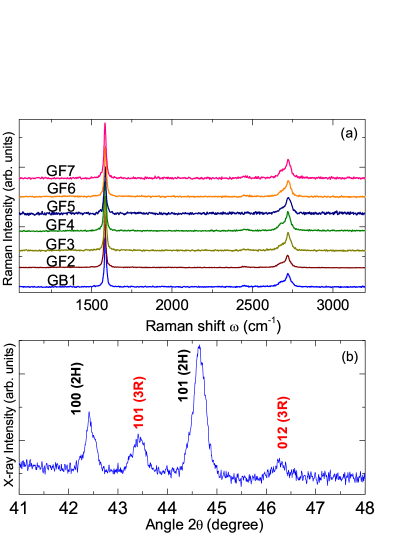
The structural quality of all samples was investigated by Raman and XRD measurements. For this purpose, a confocal micro-Raman microscope was used (alpha , WITec) with an incident laser light with nm and a maximal power of mW. The Raman results of some selected samples are shown in Fig. 1(a). The most intense peaks in the Raman spectra of graphene and graphite are expected at (the -peak) and at (the peak) Ferrari et al. (2006). The so-called -peak at is related to the disorder present in the material Ferrari and Robertson (2000); Ferrari (2007). The Raman results indicate, see Fig. 1(a), that all samples have the same structural order as the initial bulk material (sample GB1) with no evidence of disorder within experimental resolution.
The XRD measurements were done using a Bruker D8 Discover (Cu Kα radiation at 40 kV and 40 mA) with a GADDS-detector system (VÅNTEC-500). Note that there are several peaks not suitable for distinguishing both stacking modifications of graphite. Both the and of the 2H and 3R stacking are superposed. Therefore, the range was selected to determine and approximately quantify the rhombohedral phase in the samples, see Fig. 1(b), because the reflexes are not superposed in this particular range. Note, however, the reflex intensities are of the maximum relative intensity. The Rietveld refinement using TOPAS 4.2 results in wt.% for the 2H and wt.% for the 3R phase. We conclude that the presence of 3R stacking in our samples is confirmed. Scanning transmission electron microscopy (STEM) measurements for similar samples show that they are composed of many crystalline regions with aligned -axis but with different -axes orientations, i.e. twisted Bernal crystalline regions Barzola-Quiquia et al. (2008). As XRD results indicate, some of the crystalline regions have 3R stacking. Between both regions, Bernal and 3R as well as between twisted Bernal regions, interfaces are formed. Following STEM pictures Barzola-Quiquia et al. (2008); García et al. (2012) and electron back scattering diffraction (EBSD) done on similar samples González et al. (2007); García et al. (2008) the crystalline regions have in general a lateral size of the order of tenths of micrometer and a thickness varying from a few nanometers to nm. Because the percentage of 3R phase in our samples remains below 20% according the XRD results, we expect that probably the thin crystalline regions in our samples Barzola-Quiquia et al. (2008); García et al. (2012) have the 3R phase.
III Own experimental data and proposed model

The results of the temperature dependence of the normalized resistance of all investigated samples are presented in Fig. 2. Although all samples were obtained from the same initial material, different temperature dependence can be observed. Some samples show a metalliclike behavior in all temperature range, such as the GB1 (bulk), or for the multilayer graphene (MLG) flakes GF2 and GF3. Some samples exhibit a combination of metallic and semiconductinglike behavior (e.g. GF4 and GF5). The samples GF9 and GF10 show only semiconductinglike behavior with a saturation at low temperatures. The overall results are in agreement with those published earlier Barzola-Quiquia et al. (2008). At first, considering that the samples were produced using the same initial material and that the structural quality between samples does not appear to differ, the results shown in Fig. 2 are not obvious. Considering the internal structure of the initial bulk sample revealed by STEM Barzola-Quiquia et al. (2008), it is clear that the significant difference is given by the sample thickness. A dependence of the calculated resistivity on the sample thickness is shown in the inset of Fig. 2. The resistivity increases with decreasing thickness, indicating that the resistivity in relatively thick graphite samples is not constant and that these samples should not be considered as homogeneous material. In other words, the calculated resistivity using the sample geometry and resistance data should not be taken as an intrinsic value of the graphite structure. Therefore, in what follows we discuss and show resistance, not resistivity data.
The usual thickness dependence of the resistivity in metalliclike systems, such as Cu Ke et al. (2009) or Ag Tanner and Larson (1968), can be described using the theory of Fuchs-Sondheimer Fuchs (1938); Sondheimer (1952), which considers the influence of scattering processes at the sample surface. However, this does not apply for such an anisotropic material as graphite, which consists of very weakly coupled stacked layers of 2D graphene sheets, with each single graphene sheet already conducting. For the same reason and the lack of evidence of internal disorder within the MLG samples according to the Raman results, see Fig. 1, the sign change of temperature coefficient of resistance in thin graphite samples ( cannot be accounted for by enhanced electron scattering rate in analogy with the Mooij rule used to interpret the electrical conduction of disordered transition metal alloys Mooij (1973).
The decrease of the resistivity with increasing thickness can be interpreted as a consequence of the increasing metalliclike contribution of the interfaces between crystalline regions Barzola-Quiquia et al. (2008); García et al. (2012). We note that the formation of metalliclike regions at interfaces is not a new concept and was already observed in many oxide materials where even superconductivity was found at very low temperatures Reyren et al. (2007, 2009). García et al. García et al. (2012) proposed a simple, phenomenological model to understand the , which consists of two main contributions in parallel, one is originated from the interfaces and the other from the crystalline, semiconducting regions .
There should be no doubt that if the XRD results indicate that two well defined stacking orders exist in our samples, and STEM pictures show also clearly different crystalline regions Barzola-Quiquia et al. (2008); García et al. (2012); Esquinazi et al. (2014), one should take care that two-dimensional (2D) boundaries exist between those crystalline structures, embedded in the graphite sample. Moreover, 2D interfaces can occur also between twisted layers of graphene, which are characterized by a rotation angle and lateral translation. This type of 2D interfaces produces the so-called moiré patterns in the electron density of states, found on the surface of a macroscopic HOPG sample already in 1990 Kuwabara et al. (1990) and supported by several, recently done studies (for a recently published review see Esquinazi and Lysogorskiy (2016)). Our XRD results as well as other evidence Esquinazi and Lysogorskiy (2016) indicate that one cannot be sure that a transport property like the electrical resistance provides an intrinsic property of ideal graphite of the region checked between the voltage electrodes. Therefore, as a first guess we write the total measured resistance of the graphite samples as the sum of two parallel resistances formulated as García et al. (2012):
| (1) |
To obtain a good fit at low temperatures, where the metalliclike behavior overwhelms, it is necessary to assume an interface contribution to the total resistance of the form:
| (2) |
where the coefficients , , as well as the activation energy are free parameters. The temperature independent term represents the residual resistance at low temperatures. Note that this residual, temperature independent resistance is necessary to assume in the metalliclike contribution to Eq. (1), especially due to its influence at low temperatures. A similar residual, in series term is not necessary to assume in the semiconducting contribution. The linear term contribution (usually much weaker than the exponential one, i.e. ) is expected to come from the longitudinal acoustic (LA) phonon scattering Pietronero et al. (1980); Stauber et al. (2007); Park et al. (2014), for example. This contribution was already observed in graphene samples produced on Chen et al. (2008) and in suspended graphene Bolotin et al. (2008). A similar, exponential third term of Eq. (2) was already used to describe the temperature dependence of two dimensional electron-hole systems formed at the interfaces of non-conducting materials, e.g. GaAs/AlAs heterostructures Hanein et al. (1998) or -type SiGe Coleridge et al. (1997). This thermally activated contribution was first used by Kopelevich et al. Kopelevich et al. (2003) and later by Takumoto et al. Tokumoto et al. (2004) to fit the metalliclike increase in the resistance with temperature observed in bulk graphite samples. The origin of this contribution, however, remains still controversial. For example, it could be explained using a percolation of electron-hole liquid He and Xie (1998), disorder and electron-electron interactions Finkel stein (1983), or through the enhanced spin-orbit interaction by broken inversion symmetry Pudalov (1997). However, the probable origin of this thermally activated term could be related to the superconductivity localized at the interfaces between Bernal and 3R stacking. We note that a similar exponential dependence has been observed in granular Al-Ge Shapira and Deutscher (1983) for a particular Al concentration. This thermally activated behavior can be understood on the basis of the Langer-Ambegaokar-McCumber-Halperin (LAMH) model Langer and Ambegaokar (1967); McCumber and Halperin (1970) that applies to narrow superconducting channels in which thermal fluctuations can cause phase slips. The value of the activation energy meV obtained from the fits remains similar for all measured samples, see Table I.
The second term in Eq. (1) is related to the crystalline parts, which we assume to behave as intrinsic semiconductors, given by:
| (3) |
where is a mobility-dependent prefactor, is the semiconducting energy gap and is the Boltzmann constant. The temperature dependent parameter can be written as:
| (4) |
where is a temperature independent constant and and are the electron and hole mobilities. In the work of García et al. García et al. (2012), was assumed to be constant, which results of assuming , and it is a good approximation for typical semiconductors Norton et al. (1973); Canali et al. (1975).
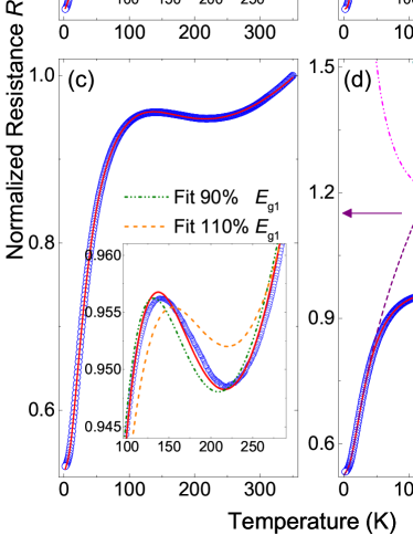
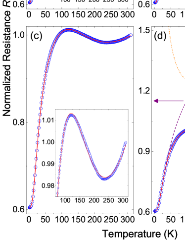
As example, we show the fitting procedure to Eq. (1) for sample GF11, see Fig. 3(a). The parameters obtained from the fittings have a maximum standard deviation of % and low correlation effects. Therefore, we restrict ourselves to show the best fits obtained after a careful test of the correlation effects between the free parameters. The assumed metalliclike contribution given by Eq. (2) fits well at low temperatures. However, in the inset we can clearly see that at higher temperatures, the fit considerably differs from the experimental data. We assume that this deviation at high temperatures is partially a consequence of the approximation that is constant. Therefore, we improve the model assuming that following experimental studies in graphite flakes García et al. (2012); Esquinazi et al. (2012). Taking this into account, we obtain and include it in Eq. (3). Using this in Eq. (1) we can fit the experimental data at high temperatures better than before (see Fig. 3(b) and its inset). In the inset we show the change of the best possible fits changing manually 10% and leaving all other parameters free.
Similar or even worse results for the other investigated samples are obtained assuming a single semiconducting contribution. From our XRD data we know that graphite is composed of two phases, Bernal and 3R stacking, and therefore we now consider these two independent and in-parallel contributions in our model to describe the temperature dependence of the resistance. For this purpose, Eq. (1) is modified by adding a new semiconducting contribution in parallel:
| (5) |
where and correspond to 3R and Bernal stacking. Using this new assumption, we can very well fit the experimental data over all temperature range for all samples, see Fig. 3(c) and Fig. 2. The contributions of each component of Eq. (5) are plotted in Fig. 3(d) as lines together with the data of sample GF11. Further example of these fits can be seen for sample GF3 in Fig. 4.
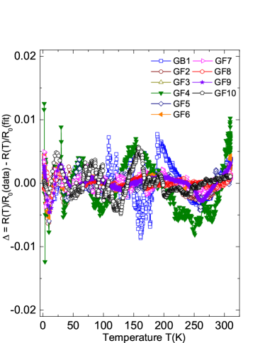
Both, the of bulk and thin MLG samples, can be very well fitted to Eq. (5) with the parameters listed in Table I. To show the accuracy of the fit of the data to Eq. (5) we plot in Fig. 5 the difference between the data and the fits defined as
| (6) |
The results in Fig. 5 indicate that the used model in this work predicts the measured normalized resistance with an accuracy better than 1% in the whole temperature range. Note that there is no systematic deviation, i.e. fluctuates around zero in the whole temperature range.
One may argue that the excellent fits to
the experimental data cannot be taken too seriously because of the large number
of free parameters, see Table I. However, a quick look at the values of the parameters
obtained from the fits of such different temperature dependences of (see Fig. 2),
indicates the following interesting facts that relativize
to some extent that argument:
(1) Regarding the interface metalliclike contribution given by Eq. (2), we note that it
defines mainly the behaviour of at temperatures K, if a metalliclike contribution
is present. The main part of the increase of with temperature (Eq. (2)) follows
always a thermally activated contribution
with an activation energy of the order of 4 meV.
(2) Although comparatively small, the introduction of
a linear in temperature term with the prefactor appears necessary.
For several samples, upon their thickness, a pure
metalliclike behavior () between 100 K and 300 K is not obvious, neither a
semiconductinglike one. It turns out that
the data showing pronounced maxima and minima cannot be well fitted without . Independently of the possible
justification based on electron-phonon interaction Pietronero et al. (1980); Stauber et al. (2007); Park et al. (2014), this term is necessary also to fit of other carbon-based materials like nanocrystal graphite thin films Cholula-Díaz
et al. (2014).
(3) In case the metalliclike interfaces contribution is negligible, e.g. sample GF10 in Fig. 2, a good fit of below K is only possible if we, as expected, neglect the thermally activated contribution and
. The negative sign of is not expected if electron-phonon interaction would play a role.
However, such a negative, nearly linear in term in especially at low temperatures,
has been observed in nano-Ag grains Liu et al. (2000) as well as in ion-beam-deposited W, Pd and Pt
nanostructures Barzola-Quiquia
et al. (2009). Its origin appears to be induced by
interfaces with very low order or disordered structures
at the interfaces between the Ag, PdC, WC and PtC nanograins. It
is appealing to suggest that the origin of this small, negative
term is related the disordered interfaces, i.e. the one to
vacuum and the one at the substrate of the FLG sample. On the
other hand, the best fit of for sample GF10 is obtained
assuming still the existence of the two stacking orders, see Table
I. In this case it is possible that not metallic but disordered
interfaces still exist in the 35 nm thick sample with a resistance
too high to play a main role in at high temperatures. Thus,
the contribution of these disordered interfaces can be seen only
at low enough temperatures, in contrast to samples where the
metalliclike interfaces dominate. Thinner samples may have only
one of the semiconducting contributions, as shown in
García et al. (2012) for a 13 nm thick HOPG sample.
(4) The behavior at K is given mainly by the semiconducting parts given by and in parallel.
(5) The values of the semiconducting energy gaps are similar for all samples with a ratio
.
(6) The weight ratio between the two semiconducting contributions given by , a value of the
order of the mass ratio between the 3R and 2H phases in our samples obtained from XRD, see Section II.
The values obtained for the activation energy are similar to those from literature Kopelevich et al. (2003); Tokumoto et al. (2004); García et al. (2012) and are, compared to 2DEG systems, one order of magnitude larger. In the work of García et al. García et al. (2012) the samples were investigated to K and the obtained semiconducting energy gap meV was attributed to the main phase of the sample, the Bernal stacking. Similar small band gaps have been observed in rhombohedral Bi Liu and Allen (1995) and alloy Saunders (1973). The values of meV obtained from the fits of for all samples are in good agreement with that of ARPES Coletti et al. (2013). Therefore, the energy gaps obtained from the fitting process can be related to the two semiconducting phases.
IV Comparison of our model with published resistance data and other theoretical models from literature
The effects of the thickness of graphite samples on the electrical properties were already studied by Ohashi et al. Ohashi et al. (1997) by cleaving a kish graphite sample with a relatively large rest resistance ratio of 32. Our results for and its thickness dependence are basically similar to those from Ohashi et al. (1997) and Barzola-Quiquia et al. (2008), compare our results in Fig. 2 and those in Figs. 6 and 7(a), i.e. the smaller the thickness of the sample the lower is the temperature where a metalliclike behavior is observed below 300 K. The model used by Ohashi et al. to interpret the obtained data is based on a two-band model and a theory for lattice vibration in thin-carbon films that includes electron-Rayleigh-wave interaction Sugihara (1988). The main assumptions of the model are: - three dimensional graphite is a semimetal because the valence band overlaps slightly the conduction band, - the degree of the overlap of these two bands depends on the film thickness and is included in the model by the free parameter , and - two relaxation rates, one due to lattice defects and the other due to lattice vibrations proportional to temperature Sugihara (1988), included in the model as the free parameter . According to this model the normalized resistance is given by the expression:
| (7) |
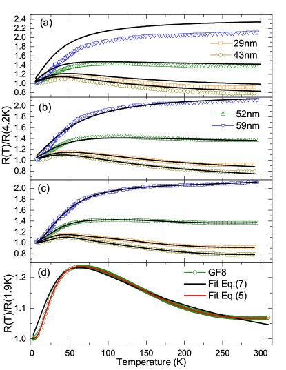
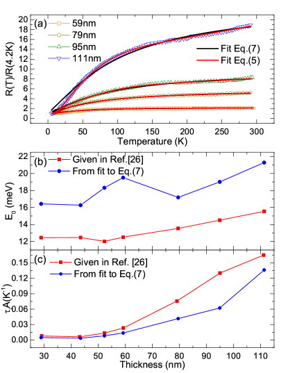
The experimental data from Ohashi et al. (1997) for samples of thickness between 111 nm and 29 nm are shown in Figs. 6 and 7(a). To check the accuracy of the fits to Eq. (7) to the authors data we show in Fig. 6(a) the data of samples with thickness between 59 nm and 29 nm taken from Ohashi et al. (1997). Using the same parameters from that publication one realizes that the fit to Eq. (7) is bad, see Fig. 6(a). Nevertheless, we left the two parameters and free and tried to get the best fits of the experimental data to Eq. (7). The results of these fits are shown in Figs. 6(b) and 7(a) and the obtained free parameters as a function of thickness are shown in Figs. 7(b) and 7(c), together with those from the original publication Ohashi et al. (1997).
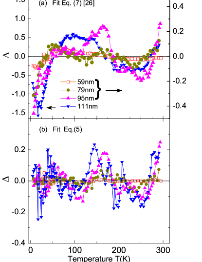
We note that the overlapping energy does show a non monotonous change with thickness, in contrast to the authors conclusion, with a maximum at a thickness around 60 nm, see Fig. 7(b). Within the assumptions of the model this behavior is not expected and it is difficult to provide any simple explanation, unless the samples with thickness between 50 nm and 60 nm would have had some peculiarities (defects, etc.) that there other samples do not. To check this speculation and also the accuracy of the fits of the data of Ohashi et al. (1997) to Eqs. (5) and (7) we show: - in Figs. 6(c) and 7(a) the fits to the Ohashi et al. data Ohashi et al. (1997) with our model, - the best fit of the data of our sample GF8 to their Eq. (7) (and to our Eq. (5)) in Fig. 6(d), - and in Fig. 8 the difference between the data and: (a) the fits using Eq. (7) from Ohashi et al. but with the best fit parameters (shown as blue circles in Fig. 7(b,c)) and (b) the fits according to our model given by Eq. (5). It is clear that the Ohashi et al. model does show systematic and much larger deviations from the experimental data (more that 100% in certain temperature range) than with our model. The parameters obtained from the fits of Ohashi et al. data to our model given by Eq. (5) are given in Table II. It is interesting to note that the obtained parameters are similar to those from the fits to our data, see Table I.
| Sample from | Thickness (nm) | (meV) | (meV) | (meV) | |||||
|---|---|---|---|---|---|---|---|---|---|
| Endo et al. (1983) | 8.2E-5 | 5.6E-4 | 127 | 38 | 5.7 | 0.96 | 0.004 | 1.55 | |
| Ohashi et al. (1997) | 29 | 4.5E-5 | 4.6E-4 | 107 | 37 | 9.8 | 0.96 | 0.0059 | 0.17 |
| Ohashi et al. (1997) | 43 | 3.4E-5 | 2.4E-4 | 109 | 33 | 12.2 | 0.98 | 0.003 | 6.29 |
| Ohashi et al. (1997) | 52 | 6.5E-5 | 4.7E-4 | 124 | 47 | 4 | 0.96 | 0.008 | 0.09 |
| Ohashi et al. (1997) | 59 | 1E-4 | 5.5E-4 | 154 | 61 | 3.7 | 0.97 | 0.0069 | 0.79 |
| Ohashi et al. (1997) | 79 | 2.9E-4 | 1.9E-3 | 116 | 35 | 2.7 | 0.66 | 0.0416 | 0.86 |
| Ohashi et al. (1997) | 95 | 5.4E-4 | 3.2E-3 | 104 | 42 | 6.5 | 0.69 | 0.0363 | 2.23 |
| Ohashi et al. (1997) | 111 | 1.6E-3 | 6.9E-3 | 104 | 42 | 6.5 | 0.71 | 0.0486 | 13.8 |
| Gutman et al. (2009) | 2.9E-4 | 2.5E-3 | 107 | 29 | 6.7 | 0.75 | 0.0371 | 1.91 |
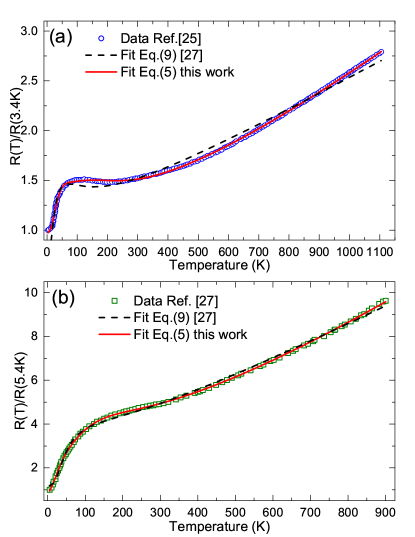
In what follows we compare one further model published by Gutman et al. Gutman et al. (2009) and our model with in-plane resistance data obtained from bulk graphite samples up to 1100 K. Figure 9 shows the experimental data of the normalized resistance vs. temperature obtained from (a) Endo et al. (1983) and (b) Gutman et al. (2009). It is interesting to note that the resistance of both samples increases with temperature above 300 K in a similar way, although according to the authors in Gutman et al. (2009), one expects a compensation between the increase in the number of carriers and the decrease in the scattering time, i.e. a saturation of the resistance. Therefore, an extra intervalley scattering of charge carriers by high-frequency, graphene-like optical phonons was assumed in Gutman et al. (2009) that provides according to those authors the necessary increase of the resistance with temperature. According to the model in Gutman et al. (2009) the resistance is given by the expression:
| (8) |
where the first term accounts for the low temperature behavior ( is the scattering rate due to impurities and due to soft phonons, similarly as in Eq. (eq:oh) and , the Fermi energy. The second term is due to intervalley scattering. Equation (8) has four free parameters, , and , being the last two the effective electron-phonon relaxation time and the frequency of the longitudinal optical mode () at the point. To fit the data of Endo et al. Endo et al. (1983) and the data of Gutman et al. Gutman et al. (2009) with this model we have used the normalized resistance following Eq. (8) as:
| (9) |
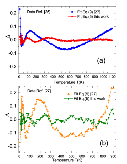
For the fit shown in Fig. 9(a) of the data of Endo et al. Endo et al. (1983) we obtained as best fit parameters: K-1, K and K=4.89 meV. in Fig. 9(b) we show the fit of the data of Gutman et al. to Eq. (9) using the same values for the free parameters as in the original publication Gutman et al. (2009). As comparison, we show in the same figures the fits of the data to our Eq. (5) with the parameters shown in Table II. For a better recognition of the differences between experimental data and fits, Fig. 10 shows the difference for both data using Eq. (9) from Gutman et al. (2009) and our Eq. (5). In this figure it is clearly observed that our model fits the resistance temperature dependence in the whole temperature range to 1100 K with a remarkable accuracy, better than 5% (relative) and without any systematic deviation from the main experimental temperature behaviour, in contrast to the model given by Eq. (9). From all these results we may conclude that the increase of in graphite is due to the temperature increase expected for a small-gap semiconducting material with a mobility that decreases with temperature as .
V Conclusion
Concluding, we have investigated the longitudinal resistance of a bulk and a series of mesoscopic graphite samples obtained from the same initial material with similar structural quality. Our results show that the transport properties of bulk graphite are not unique, as they depend strongly upon the amount of interfaces present in the material. By fitting the temperature dependence of the resistance we found indications for the contribution of the semiconducting rhombohedral phase with an energy gap similar to the one reported in literature. XRD measurements reveal the presence of the rhombohedral and Bernal phases in the graphite material used in our experiments. From our interpretation we can conclude that the metalliclike contribution to the electrical resistance is not intrinsic of ideal graphite but due to interfaces between, e.g., Bernal and 3R stacking.
Independently of the fit parameters used, none of the published models can fit as accurate as the one proposed in this study. The available data from literature and in a broad temperature range indicate also the existence of the two stacking orders with similar energy gaps as the samples studied in this work.
We note that these interfaces
might be the reason for the superconductinglike behavior at very
high temperatures observed in the magnetization of bulk and
treated graphite powders Kopelevich et al. (2000); Scheike et al. (2012, 2013), in the
transport properties of TEM graphite lamellae where a direct
contact to the interfaces has been achieved Ballestar et al. (2013), as well
as in stapled graphite flakes Kawashima (2013).
Acknowledgments: We acknowledge fruitful discussions with T. Heikkilä, G. Volovik and Y. Kopelevich.
References
- Bernal (1924) J. D. Bernal, Proc. R. Soc. Lond. A 106, 749 (1924).
- Lipson and Stokes (1942) H. Lipson and A. R. Stokes, Proc. R. Soc. Lond. A 181, 101 (1942).
- Kelly (1981) B. T. Kelly, Physics of Graphite (London: Applied Science Publishers, 1981).
- Lui et al. (2011) C. H. Lui, Z. Li, Z. Chen, P. V. Klimov, L. E. Brus, and T. F. Heinz, Nano Lett. 11, 164 (2011).
- Matuyama (1956) E. Matuyama, Nature 178, 1459 (1956).
- Freise and Kelly (1963) E. J. Freise and A. Kelly, Philos. Mag. A 8, 1519 (1963).
- Wallace (1947a) P. R. Wallace, Phys. Rev. 71, 622 (1947a).
- Wallace (1947b) P. R. Wallace, Phys. Rev. 72, 258 (1947b).
- Mrozowski (1952) S. Mrozowski, Phys. Rev. 85, 609 (1952).
- Mrozowski (1950) S. Mrozowski, Phys. Rev. 77, 838 (1950).
- Guinea et al. (2006) F. Guinea, A. C. Neto, and N. M. R. Peres, Phys. Rev. B 73, 245426 (2006).
- Koshino and McCann (2009) M. Koshino and E. McCann, Phys. Rev. B 80, 165409 (2009).
- Koshino (2010) M. Koshino, Phys. Rev. B 81, 125304 (2010).
- Coletti et al. (2013) C. Coletti, S. Forti, A. Principi, K. V. Emtsev, A. A. Zakharov, K. M. Daniels, B. K. Daas, M. V. S. Chandrashekhar, T. Ouisse, D. Chaussende, et al., Phys. Rev. B 88, 155439 (2013).
- Dutta (1953) A. K. Dutta, Phys. Rev. 90, 187 (1953).
- Reynolds et al. (1953) J. M. Reynolds, H. W. Hemstreet, and T. E. Leinhardt, Phys. Rev. 91, 1152 (1953).
- Kopnin et al. (2011) N. B. Kopnin, T. T. Heikkilä, and G. E. Volovik, Phys. Rev. B 83, 220503 (2011).
- Pierucci et al. (2015) D. Pierucci, H. Sediri, M. Hajlaoui, J.-C. Girard, T. Brumme, M. Calandra, E. Velez-Fort, G. Patriarche, M. G. Silly, G. Ferro, et al., ACS Nano 9, 5432 (2015).
- Heikkilä et al. (2011) T. T. Heikkilä, N. B. Kopnin, and G. E. Volovik, JETP Lett. 94, 233 (2011).
- Heikkilä and Volovik (2011) T. T. Heikkilä and G. E. Volovik, JETP Lett. 93, 59 (2011).
- Kopnin et al. (2013) N. B. Kopnin, M. Ijäs, A. Harju, and T. T. Heikkilä, Phys. Rev. B 87, 140503 (2013).
- Kopnin and Heikkilä (2015) N. B. Kopnin and T. T. Heikkilä, Carbon-based Superconductors: Towards High- Superconductivity (Pan Stanford Publishing, CRC Press, Taylor & Francis Group, 2015), chap. 9, pp. 231–263, arXiv:1210.7075.
- Muñoz et al. (2013) W. A. Muñoz, L. Covaci, and F. Peeters, Phys. Rev. B 87, 134509 (2013).
- Esquinazi et al. (2014) P. Esquinazi, T. T. Heikkilä, Y. V. Lysogoskiy, D. A. Tayurskii, and G. E. Volovik, JETP Letters 100, 336 (2014), arXiv:1407.1060.
- Endo et al. (1983) M. Endo, T. Chieu, G. Timp, , M. Dresselhaus, and B. S. Elman, Phys. Rev. B 28, 6982 (1983).
- Ohashi et al. (1997) Y. Ohashi, T. Koizumi, T. Yoshikawaa, T. Hironaka, and K. Shiiki, TANSO 180, 235 (1997).
- Gutman et al. (2009) D. Gutman, S. Tongay, H. Pal, D. Maslov, and A. Hebard, Phys. Rev. B 80, 045418 (2009).
- Spemann et al. (2014) D. Spemann, P. Esquinazi, A. Setzer, and W. Böhlmann, AIP Advances 4, 107142 (2014).
- Barzola-Quiquia et al. (2008) J. Barzola-Quiquia, J.-L. Yao, P. Rödiger, K. Schindler, and P. Esquinazi, phys. stat. sol. a 205, 2924 (2008).
- Ferrari et al. (2006) A. C. Ferrari, J. C. Meyer, V. Scardaci, C. Casiraghi, M. Lazzeri, F. Mauri, S. Piscanec, D. Jiang, K. S. Novoselov, S. Roth, et al., Phys. Rev. Lett. 187401, 97 (2006).
- Ferrari and Robertson (2000) A. C. Ferrari and J. Robertson, Phys. Rev. B 14095, 61 (2000).
- Ferrari (2007) A. C. Ferrari, Solid State Commun 143, 47 (2007).
- García et al. (2012) N. García, P. Esquinazi, J. Barzola-Quiquia, and S. Dusari, New Journal of Physics 14, 053015 (2012).
- González et al. (2007) J. C. González, M. Muñoz, N. García, J. Barzola-Quiquia, D. Spoddig, K. Schindler, and P. Esquinazi, Phys. Rev. Lett. 99, 216601 (2007).
- García et al. (2008) N. García, P. Esquinazi, J. Barzola-Quiquia, B. Ming, and D. Spoddig, Phys. Rev. B 78, 035413 (2008).
- Ke et al. (2009) Y. Ke, F. Zahid, V. Timoshevskii, K. Xia, D. Gall, and H. Guo, Phys. Rev. B 79, 155406 (2009).
- Tanner and Larson (1968) D. Tanner and D. Larson, Phys. Rev. 166, 652 (1968).
- Fuchs (1938) K. Fuchs, Cambridge Philos. Soc. 34, 100 (1938).
- Sondheimer (1952) E. Sondheimer, Adv. Phys. 1, 1 (1952).
- Mooij (1973) J. H. Mooij, Phys. Stat. Sol. (a) 17, 521 (1973).
- Reyren et al. (2007) N. Reyren, S. Thiel, A. D. Caviglia, L. F. Kourkoutis, G. Hammerl, C. Richter, C. W. Schneider, T. Kopp, A.-S. Rüetschi, D. Jaccard, et al., Science 317, 1196 (2007).
- Reyren et al. (2009) N. Reyren, S. Gariglio, A. D. Caviglia, D. Jaccard, T. Schneider, and J.-M. Triscone, Appl. Phys. Lett. 94, 112506 (2009).
- Kuwabara et al. (1990) M. Kuwabara, D. R. Clarke, and A. A. Smith, Appl. Phys. Lett. 56, 2396 (1990).
- Esquinazi and Lysogorskiy (2016) P. Esquinazi and Y. Lysogorskiy, Chapter 7 in Basic Physics of Functionalized Graphite, Springer Series in Materials Science (Springer International Publishing, 2016), ISBN 978-3-319-39353-7.
- Pietronero et al. (1980) L. Pietronero, S. Strässler, and H. Z. M. Rice, Phys. Rev. B 22, 904 (1980).
- Stauber et al. (2007) T. Stauber, N. M. R. Peres, and F. Guinea, Phys. Rev. B 76, 205423 (2007).
- Park et al. (2014) C.-H. Park, N. Bonini, T. Sohier, G. Samsonidze, B. Kozinsky, M. Calandra, F. Mauri, and N. Marzari, Nano Lett. 14, 1113 (2014).
- Chen et al. (2008) J.-H. Chen, C. Jang, S. Xia, M. Ishigami, and M. S. Fuhrer, Nature Nanotechnology 3, 206 (2008).
- Bolotin et al. (2008) K. I. Bolotin, K. J. Sikes, J. Hone, H. L. Stormer, and P. Kim, Phys. Rev. Lett. 101, 096802 (2008).
- Hanein et al. (1998) Y. Hanein, U. Meirav, D. Shahar, C. C. Li, D. C. Tsui, and H. Shtrikman, Phys. Rev. Lett. 80, 1228 (1998).
- Coleridge et al. (1997) P. T. Coleridge, R. L. Williams, Y. Feng, and P. Zawadzki, Phys. Rev. B 56, R12764(R) (1997).
- Kopelevich et al. (2003) Y. Kopelevich, P. Esquinazi, J. Torres, R. da Silva, H. Kempa, F. Mrowka, and R. Ocaña, Studies of High-Temperature Superconductors (Nova Science Publishers, Inc., 2003), vol. 45, chap. 3, pp. 59–106.
- Tokumoto et al. (2004) T. Tokumoto, E. Jobiliong, E. Choi, Y. Oshima, and J. Brooks, Solid State Commun. 129, 599 (2004).
- He and Xie (1998) S. He and X. C. Xie, Phys. Rev. Lett. 80, 3324 (1998).
- Finkel stein (1983) A. M. Finkel stein, Zh. Eksp. Teor. Fiz. 84, 168 (1983).
- Pudalov (1997) V. M. Pudalov, JETP Lett. 66, 175 (1997).
- Shapira and Deutscher (1983) Y. Shapira and G. Deutscher, Phys. Rev. B 27, 4463 (1983).
- Langer and Ambegaokar (1967) J. S. Langer and V. Ambegaokar, Phys. Rev. 164, 498 (1967).
- McCumber and Halperin (1970) D. E. McCumber and B. I. Halperin, Phys. Rev. B 1, 1054 (1970).
- Norton et al. (1973) P. Norton, T. Braggins, and H. Levinstein, Phys. Rev. B 8, 5632 (1973).
- Canali et al. (1975) C. Canali, C. Jacoboni, F. Nava, G. Ottaviani, and A. Alberigi-Quaranta, Phys. Rev. B 12, 2265 (1975).
- Esquinazi et al. (2012) P. Esquinazi, J. Barzola-Quiquia, S. Dusari, and N. Garcia, J. Appl. Phys. 111, 033709 (2012).
- Cholula-Díaz et al. (2014) J. L. Cholula-Díaz, J. Barzola-Quiquia, H. Krautscheid, U. Teschner, and P. Esquinazi, Carbon 67, 10 (2014).
- Liu et al. (2000) Y. Liu, C. Mo, and W. Cai, J. Mater. Sei. Techno. 16, 521 (2000).
- Barzola-Quiquia et al. (2009) J. Barzola-Quiquia, S. Schulze, and P. Esquinazi, Nanotechnology 20, 165704 (2009).
- Liu and Allen (1995) Y. Liu and R. E. Allen, Phys. Rev. B 52, 1566 (1995).
- Saunders (1973) G. A. Saunders, Contemporary Physics 14, 149 (1973).
- Sugihara (1988) K. Sugihara, Phys. Rev. B 37, 7063 (1988).
- Kopelevich et al. (2000) Y. Kopelevich, P. Esquinazi, J. Torres, and S. Moehlecke, J. Low Temp. Phys. 119, 691 (2000).
- Scheike et al. (2012) T. Scheike, W. Böhlmann, P. Esquinazi, J. Barzola-Quiquia, A. Ballestar, and A. Setzer, Adv. Mater. 24, 5826 (2012).
- Scheike et al. (2013) T. Scheike, P. Esquinazi, A. Setzer, and W. Böhlmann, Carbon 59, 140 (2013).
- Ballestar et al. (2013) A. Ballestar, J. Barzola-Quiquia, T. Scheike, and P. Esquinazi, New J. Phys. 15, 023024 (2013).
- Kawashima (2013) Y. Kawashima, AIP Advances 3, 052132 (2013).