Photon-assisted tunneling and charge dephasing in a carbon nanotube double quantum dot
Abstract
We report microwave-driven photon-assisted tunneling in a suspended carbon nanotube double quantum dot. From the resonant linewidth at a temperature of 13 mK, the charge dephasing time is determined to be ps. The linewidth is independent of driving frequency, but increases with increasing temperature. The moderate temperature dependence is inconsistent with expectations from electron-phonon coupling alone, but consistent with charge noise arising in the device. The extracted level of charge noise is comparable with that expected from previous measurements of a valley-spin qubit, where it was hypothesized to be the main cause of qubit decoherence. Our results suggest a possible route towards improved valley-spin qubits.
I Introduction
Qubit manipulation in carbon nanotube devices is of interest both for quantum computing Churchill et al. (2009); Flensberg and Marcus (2010); Pályi and Burkard (2011); Pei et al. (2012) and for coherent control of nanomechanical states via strong coupling to a spin qubit Pályi et al. (2012); Ohm et al. (2012). The low concentration of nuclear spins in carbon is at first sight promising for spin and valley coherence, but the qubit coherence time observed so far Laird et al. (2013); Viennot et al. (2014) has not exceeded 100 ns, well below the expected limit from electron-lattice and spin-orbit coupling Bulaev et al. (2008); Rudner and Rashba (2010). Instead, it is possible that this coherence is limited by charge dephasing, with a coupling to valley-spin states arising from spin-orbit coupling or gate-voltage dependent inter-dot exchange Li et al. (2014); Laird et al. (2015).
Here, we probe charge dephasing by measuring photon-assisted tunneling (PAT) Meyer et al. (2007) for the first time in a carbon nanotube double quantum dot. This effect occurs when energy absorbed from a microwave electric field stimulates charge tunneling between quantum dots that would otherwise be suppressed by Coulomb blockade. Because PAT is a resonant effect, the measured width of the absorption line is proportional to the charge dephasing rate. By measuring the frequency and temperature dependence of the PAT resonance linewidth, we deduce that in this device, low-temperature charge dephasing is limited mainly by electrical noise, with possible contribution from phonon coupling above 50 mK, and with electron tunneling excluded as the dominant mechanism. The noise level deduced from the dephasing rate is of the same order of magnitude as estimated previously to account for dephasing of the nanotube valley-spin qubit Laird et al. (2013).
II Photon-assisted tunneling
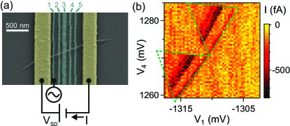
To fabricate the double quantum dot [Fig. 1(a)], a carbon nanotube is synthesized by chemical vapour deposition on a quartz chip using FeCl as a catalyst Zhou et al. (2008). On a separate chip, consisting of intrinsic Si substrate with 300 nm thermal oxide, 20 nm thick Cr/Au gates (labelled 1-5) are patterned, followed by 130 nm thick Cr/Au contact electrodes to define a trench. The nanotube is transferred by stamping Wu et al. (2010); Pei et al. (2012) so that it is suspended over the trench between the two contacts. The device is measured in a dilution refrigerator with a base temperature of 13 mK. Electron thermalization is achieved by heat-sinking all dc via printed circuit board copper powder filters containing stages with kHz cutoff Mueller et al. (2013). To allow a microwave signal to be added to the DC gate voltage, Gate 1 is connected via a bias tee to a microwave source via a section of NbTi superconducting coaxial cable fitted with cold attenuators totalling 28 dB.
A double quantum dot defined through a combination of Schottky barriers at the contacts and DC gate voltages, which together deplete three short segments of the nanotube so as to create a double-well potential. The gate voltages are set so that the double dot is measured in the configuration, where both quantum dots are occupied by holes. The chemical potentials in the left and right dots are adjusted by sweeping gate voltages and , applied to gates 1 and 4 respectively. Hole tunneling through the three tunnel barriers gives rise to a currnet through the nanotube. With a bias applied between the contacts, and with microwaves turned off, the current is shown in Fig. 1(b) as a function of and . For most gate voltage settings, the alignment of energy levels in the two quantum dots means that hole tunneling is suppressed by Coulomb blockade. The two triangles of allowed current are characteristic of a double quantum dot van der Wiel et al. (2003).
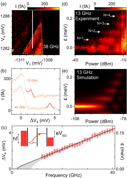
To detect PAT, the current is measured with microwaves applied [Fig. 2(a)]. A line of microwave-induced current [marked by an arrow in Fig. 2(a)] appears outside the transport triangle, in a region of gate space where Coulomb blockade suppresses current in the absence of microwaves. For these gate voltage settings, Coulomb blockade is broken by photon absorption Oosterkamp et al. (1998) allowing a hole to tunnel uphill from left to right between two resonant levels and subsequently escape to the right lead [Fig. 2(c) inset]. Measuring the position of this line as a function of microwave frequency allows spectroscopy of the double quantum dot. With the detuning defined as the difference in hole chemical potentials between right and left dots, a current peak is expected whenever , where is the energy difference between bonding and antibonding states of the double dot, is an integer, and is Planck’s constant.
This PAT spectroscopy is seen in Fig. 2(b), which shows peaks for two different microwave frequencies. The current is plotted against gate voltage location , defined along the line marked in Fig. 2(a). With the origin of this set at the triangle baseline, where the chemical potentials of left and right dots are equal, detuning is related to gate voltage by , where is the lever arm between gete voltage and detuning. As expected, the peak moves towards greater detuning with higher frequency. To characterize this behaviour in more detail, we fit the current peak at each frequency with a Lorentzian, including an offset slope to account for background current. The fitted peak centers are plotted in Fig. 2(c). The dependence of peak detuning on frequency is approximately linear, consistent with a weakly tunnel-coupled double dot. The data are fitted to the equation expected from a two-level model Oosterkamp et al. (1998):
| (1) |
where is the electron charge, with and the inter-dot tunnel coupling taken as fit parameters. As seen, the spectroscopic effect of the tunnel coupling eV is negligible within the uncertainty. The lever arm is consistent with that obtained from the size of the bias triangle in Fig. 2(a) van der Wiel et al. (2003).
With increased microwave power, multi-photon transitions can be observed [Fig. 2(d)]. The dependence on detuning and power is in reasonable agreement with a model of resonant transitions with dephasing Stoof and Nazarov (1996) [Fig. 2(e) and Appendix A]. In particular, the dependence of current on power is weakly non-monotonic, an indication of interference between different coherent transitions. However, this effect is masked by a non-resonant current increase at high power, presumably reflecting incoherent tunneling due to heating. The power offset between simulation and data allows the ratio between the generator output and quantum dot detuning to be extracted, which at this frequency is 68 dB. For the following data the power is set well below the threshold for multi-photon processes.
III Charge dephasing
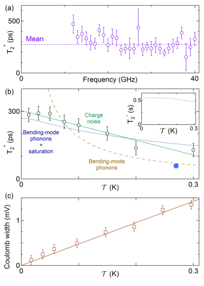
By studying PAT as a function of frequency and fridge temperature , information about charge dephasing and hence about the electrical environment can be obtained. The dephasing time is extracted from the width of the PAT peak in detuning Petta et al. (2004) using the formula , where is the full width at half maximum of the Lorentzian. Figure 3(a) shows as a function of microwave frequency at mK, obtained from fits as in Fig. 2(b). The mean value is ps, similar to measurements in GaAs quantum dots Hayashi et al. (2003); Petta et al. (2004); Frey et al. (2012), Si donors Dupont-Ferrier et al. (2013), and nanotube circuit-quantum-electrodynamics devices Viennot et al. (2015); Ranjan et al. (2015). Both in this data and at higher temperatures (not shown), no strong dependence on frequency is seen. Figure 3(b) shows the temperature dependence of averaged over the entire measured frequency range. As expected, decreases at higher temperature, indicating thermally activated dephasing mechanisms.
To confirm proper thermalization of the device, Fig. 3(c) shows the measured width of a Coulomb step feature (the edge of a bias triangle similar to Fig. 2(a)) as a function of temperature with no microwaves applied. Because this step is broadened by thermal smearing in the leads, the linear dependence indicates that the electron temperature closely tracks .
IV Mechanisms of dephasing
In this section, we compare the data of Fig. 3(a-b) with expectations from various charge dephasing processes in this device Hayashi et al. (2003). We consider first vibrational dephasing, by analysing the phonon spectrum and dominant coupling mechanisms to the charge state. We must consider both bending and stretching modes as potential contributors to charge dephasing. For the former, coupling to the charge state arises from displacement of the quantum dots in the gate electric field, whereas the electron-phonon coupling of longitudinal phonons arises from the deformation potential. The spectra of bending and stretching phonons are (neglecting tension) given by Suzuura and Ando (2002); Ando (2005); Bulaev et al. (2008); Rudner and Rashba (2010):
| (2) | ||||
| (3) |
where is the longitudinal sound velocity and and are the radius and length of the suspended nanotube. Estimating nm and using nm results in MHz and GHz for the lowest frequency bending and stretching mode.
The respective electron-phonon couplings for bending and stretching modes are calculated in Appendix B:
| (4) | ||||
| (5) |
Numerical estimates considering the underlying mechanisms Sup give (assuming an electric field based on applied gate voltage and sample geometry, and nanotube mass kg), and . In both cases the coupling strength peaks for the lowest frequency mode.
Dephasing will thus be dominated by thermally populated low-frequency modes. Contrary to a previous treatment of double dot electron-phonon coupling Hayashi et al. (2003) based on the canonical spin-boson model with quasi-continuous spectral density Leggett et al. (1987), we anticipate that only a small number of modes is relevant in this case, suggesting a different approach is required. To estimate , we therefore adapt analytically derived Rabi-model dephasing rates Fruchtman et al. (2015). These rely upon a perturbative expansion utilising the phase space representation of the oscillators. In our case the charge dephasing rate due to a single phonon mode with coupling is
| (6) |
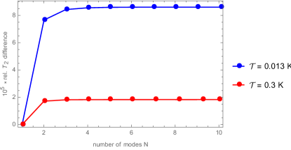
with being Boltzmann’s constant, the phonon relaxation rate, and the charge qubit energy splitting. In contrast to the spin-boson model, where the loss of coherence is determined by the spectral density Brandes (2005), Eq. (6) explicitly includes the finite lifetime of the relevant phonon modes, as well as the charge bias and tunneling. Generalisation to multiple modes is straightforward Fruchtman et al. (2015) but unnecessary here: for the parameters discussed below inclusion of up to 10 modes gives relative changes of less than (Appendix C).
Figure 3(b) shows a fit of calculated using Eq. (6) for the lowest frequency bending mode, where in Eq. (4) is taken as the fitting parameter. For the frequency of the lowest mode, measured electromechanically Sazonova et al. (2004); Ares et al. (2016), we take MHz and from the linewidth . The higher value of than in Eq. (2) presumably reflects tension in the suspended nanotube Sapmaz et al. (2003). The fit yields , in reasonable agreement with the previous estimate given the many uncertainties. By contrast, the lowest stretching mode [using Eqs. (3) and (5)] leads to dephasing on a timescale approaching seconds [Fig. 3(b)inset] and can therefore be ruled out. The calculated shows almost no dependence on in the measured temperature range, consistent with Fig. 3(a). Bearing in mind that Eq. (6) relies on a perturbative expansion of electron-phonon coupling, we have checked that full numerical simulations of a single mode Rabi model using QuTip Johansson et al. (2013) lead to a temperature dependence in the dephasing time that is consistent with Eq. (6) (Appendix C).
Thus, while bending mode phonons may limit above mK, they cannot explain the measurements across the entire temperature range due to the strong temperature dependence of the phonon model. This suggests that at least at low temperatures a different mechanism limiting coherence must be at play. We therefore next compare with expectations from electrical noise. In this case, the dephasing time is given by , where is the root-mean-square detuning noise at frequencies up to the driving frequency Laird et al. (2013). Assuming that the noise spectrum is dominated by frequencies below 10 GHz, this is consistent with the data in Fig. 3(a) if meV at low . There is no clear expectation for the temperature dependence; however, in a GaAs spin qubit device where dephasing was attributed to thermally activated electrostatic noise, an approximately linear dependence of on was found Dial et al. (2013). This simple model fits the data well [Fig. 3(b)], meaning charge noise cannot be excluded as the limit of across the temperature range.
Thirdly, we suppose that phonon-mediated dephasing operates in conjunction with some other mechanism, such as temperature-independent charge noise. To model these two mechanisms combining incoherently, we fit the data in Fig. 3(b) across the entire range with
| (7) |
where is the phonon dephasing time given by Eq. (6) and ps is a saturation value taken as equal to the measured at 13 mK. This model also fits the data well with .
Finally, we consider that is set by the lifetime of the excited state, limited by tunneling to the leads. Because escape from the right dot is not Coulomb-blocked [Fig. 2(c) inset], this effect should show no strong temperature dependence, and therefore is not the main limit on . Furthermore, we observe no dependence of on gate voltage tuning, indicating that it is not affected by tunnel barriers as tunneling or cotunneling would be. In conclusion, we deduce that charge coherence is limited by electrical noise at low temperatures, with a possible contribution from phonons above 50 mK.
V Conclusion
Because PAT spectroscopy gives a direct measurement of the charge dephasing rate, it may shed light on the cause of dephasing for a valley-spin qubit defined in a similar device Laird et al. (2013). In that experiment, performed at 270 mK, a voltage-dependent spin splitting made the qubit sensitive to electrical noise, which was suggested as the main limit on the decoherence rate. To explain the measured valley-spin decoherence rate, an rms detuning jitter meV was required. In Fig. 3(b), the charge expected from the same detuning jitter is plotted as a filled circle, and is found to be of the same order of magnitude as measured here. It is therefore plausible that charge noise was a contributor to the decoherence and dephasing rates measured for that valley-spin qubit Laird et al. (2013).
The origin of the noise remains unclear. The required noise level is far in excess of expectation from our room-temperature electronics. The fact that the noise is apparently reduced compared with that in Ref. Laird et al. (2013) (where the nanotube rested on an oxide layer) suggests a contribution from the substrate. However, in our device most substrate noise should be screened by the surface gates. One origin could be electrostatic patch noise on the electrode surfaces, as seen in ion traps Wineland et al. (1998). Another is possible presence of fluctuating charge traps on the surface of the nanotube itself, either in amorphous carbon deposited during synthesis, or from adsorbed water Kim et al. (2003). These results suggest that, provided other decoherence mechanisms such as magnetic 13C nuclear impurities can be eliminated, careful control of nanotube synthesis and/or vacuum conditions in the cryostat may enhance both charge and valley-spin coherence in nanotube quantum dots.
VI Acknowledgements
We acknowledge N. Ares, C.S. Allen, and Y. Li for discussions, and support from EPSRC (EP/J015067/1), Templeton World Charity Foundation, a Marie Curie Career Integration Grant, the Royal Society of Edinburgh and Scottish Government, and the Royal Academy of Engineering.
Appendix A Photon-assisted tunneling with dephasing
The simulation in Fig. 2(e) uses a model of time-dependent resonant tunneling between two states Stoof and Nazarov (1996), with the phenomenogical inclusion of a level-broadening term due to dephasing. The current is:
| (8) |
where is the microwave voltage at the signal generator, is the corresponding detuning variation, and an overall scaling factor (set by the double-dot tunnel couplings). Here is the insertion loss between generator and device, including attenuators, cable losses, and the gate lever arm. To generate Fig. 2(e) was set to 300 ps and and were adjusted by hand to match the data. By this procedure is estimated at 68 dB, consisting of 28 dB from the inline attenuators, dB from the lever arm, and dB from losses in room-temperature cable and the sample holder.
Appendix B Electron-phonon coupling constants
Our starting point is the spin-boson Hamiltonian Leggett et al. (1987); Brandes (2005):
| (9) |
with bare double dot represented by a pseudo-spin Hamiltonian
| (10) |
where and for representing the presence of the hole on the left or the right dot, respectively. Each phonon mode with wavevector , angular frequency , and ladder operators is governed by the Hamiltonian of the harmonic oscillator
| (11) |
and the charge-phonon coupling given by
| (12) |
Here the electron-phonon coupling in each mode is parameterized by .
To estimate we express the oscillator displacement for each wavevector in terms of the (real-space) position variable ,
| (13) |
where is the mass of the nanotube. Two physical mechanisms contribute to the electron-phonon interaction: coupling to bending-mode phonons via the gate electric field and coupling to longitudinal phonons via the deformation potential Ando (2005); Suzuura and Ando (2002); Rudner and Rashba (2010); Bulaev et al. (2008). We estimate them in turn.
B.1 Bending-mode phonons
The bending-mode dispersion relation Bulaev et al. (2008) is , with , where and are the radius and length of the nanotube. The deformation potential associated with these phonons averages to zero around the nanotube circumference Bulaev et al. (2008), so electron-phonon coupling arises mainly from the perpendicular electric field induced by the gates. This mediates coupling to bending-mode phonons according to the Hamiltonian
| (14) |
where is a form factor that parameterizes the average displacement over the length of a quantum dot Golovach et al. (2004). Equating Eq. (14) with Eq. (12) gives
| (15) |
B.2 Longitudinal phonons
For longitudinal phonons, we must consider both stretching and torsional modes, with each mode coupling via both diagonal and off-diagonal matrix elements in sublattice space Ando (2005). The dominant term is the diagonal coupling to stretching-mode phonons, whose dispersion relation is . The deformation potential Hamiltonian in this case leads to Bulaev et al. (2008)
| (16) |
where the coupling constant is eV. Equating Eqs. (16) and (12) gives
| (17) |
For torsional modes, the dispersion relation is similar and the coupling constant is about an order of magnitude smaller Bulaev et al. (2008). These can therefore be neglected.
Since and are out of phase, the mechanisms decouple to second order and can be treated independently.
Appendix C Approximation of dephasing time
Ref. Fruchtman et al., 2015 allows us obtain an analytical estimate of the ‘spin’ coherence time in the presence of one or more oscillator modes. This is more appropriate than solutions to the canonical spin-boson model, as the discrete oscillator environment is too small to assume short environmental correlations times. By contrast, the phase space representation technique Fruchtman et al. (2015) is capable of resolving non-Markovian dynamics of combined charge qubit and oscillator(s). Note that in our case the qubit dephasing will be predominantly caused by oscillator relaxation.
The main text only considers the lowest frequency mode. To verify the validity of this simplification, Fig. 4 shows the effect on the predicted dephasing time as the next higher frequency modes are included at both the lowest and the highest temperature of the experiment. In both cases the relative shortening of the dephasing time is smaller than .
At low temperature, we can also solve the full dynamics of Hamiltonian (9) numerically, for example using a package like QuTip Johansson et al. (2013). However, rigorously extracting a dephasing time is not straightforward: time traces of the charge qubit’s coherence are rich in features over a long time in the relevant parameter regime, leading to a rather messy Fourier spectrum. A possible way of extracting a crude estimate of the dephasing time is to consider the amplitude range of coherence oscillations over ten Rabi periods , and finding the smallest for which .
In the low temperature regime K (where the Hilbert space can be safely truncated at below 100 excitations) a single mode Rabi model with parameters as in the main text shows a temperature dependence in the decay of the qubit coherence that is consistent with the predictions of Eq. (6) in the main text. We therefore conclude that the qualitative predictions of Eq. (6) are indeed adequate for ruling out phonons as the origin of low temperature charge dephasing.
References
- Churchill et al. (2009) H. O. H. Churchill, F. Kuemmeth, J. Harlow, A. Bestwick, E. I. Rashba, K. Flensberg, C. Stwertka, T. Taychatanapat, S. Watson, and C. M. Marcus, Phys. Rev. Lett. 102, 166802 (2009).
- Flensberg and Marcus (2010) K. Flensberg and C. M. Marcus, Phys. Rev. B 81, 195418 (2010).
- Pályi and Burkard (2011) A. Pályi and G. Burkard, Phys. Rev. Lett. 106, 86801 (2011).
- Pei et al. (2012) F. Pei, E. A. Laird, G. A. Steele, and L. P. Kouwenhoven, Nature Nanotech. 7, 630 (2012).
- Pályi et al. (2012) A. Pályi, P. Struck, M. Rudner, K. Flensberg, and G. Burkard, Phys. Rev. Lett. 108, 206811 (2012).
- Ohm et al. (2012) C. Ohm, C. Stampfer, J. Splettstoesser, and M. R. Wegewijs, Appl. Phys. Lett. 100, 143103 (2012).
- Laird et al. (2013) E. A. Laird, F. Pei, and L. P. Kouwenhoven, Nature Nanotech. 8, 565 (2013).
- Viennot et al. (2014) J. J. Viennot, M. R. Delbecq, M. C. Dartiailh, A. Cottet, and T. Kontos, Phys. Rev. B 89, 165404 (2014).
- Bulaev et al. (2008) D. V. Bulaev, B. Trauzettel, and D. Loss, Phys. Rev. B 77, 235301 (2008).
- Rudner and Rashba (2010) M. S. Rudner and E. I. Rashba, Phys. Rev. B 81, 125426 (2010).
- Li et al. (2014) Y. Li, S. C. Benjamin, G. A. D. Briggs, and E. A. Laird, Phys. Rev. B 90, 195440 (2014).
- Laird et al. (2015) E. A. Laird, F. Kuemmeth, G. A. Steele, K. Grove-Rasmussen, J. Nygård, K. Flensberg, and L. P. Kouwenhoven, Rev. Mod. Phys. 87, 703 (2015).
- Meyer et al. (2007) C. Meyer, J. Elzerman, and L. P. Kouwenhoven, Nano Lett. 7, 295 (2007).
- Zhou et al. (2008) W. Zhou, C. Rutherglen, and P. J. Burke, Nano Research 1, 158 (2008).
- Wu et al. (2010) C.-C. Wu, C. H. Liu, and Z. Zhong, Nano Lett. 10, 1032 (2010).
- Mueller et al. (2013) F. Mueller, R. N. Schouten, M. Brauns, T. Gang, W. H. Lim, N. S. Lai, A. S. Dzurak, W. G. van der Wiel, and F. A. Zwanenburg, Rev. Sci. Inst. 84, 044706 (2013).
- van der Wiel et al. (2003) W. G. van der Wiel, S. De Franceschi, J. M. Elzerman, T. Fujisawa, S. Tarucha, and L. P. Kouwenhoven, Rev. Mod. Phys. 75, 1 (2003).
- Oosterkamp et al. (1998) T. H. Oosterkamp, T. Fujisawa, W. Wiel, K. Ishibashi, R. V. Hijman, S. Tarucha, and L. P. Kouwenhoven, Nature 395, 873 (1998).
- Stoof and Nazarov (1996) T. Stoof and Y. V. Nazarov, Phys. Rev. B 53, 1050 (1996).
- Petta et al. (2004) J. R. Petta, A. C. Johnson, C. M. Marcus, M. P. Hanson, and A. C. Gossard, Phys. Rev. Lett. 93, 186802 (2004).
- Hayashi et al. (2003) T. Hayashi, T. Fujisawa, H.-D. Cheong, Y.-H. Jeong, and Y. Hirayama, Phys. Rev. Lett. 91, 226804 (2003).
- Frey et al. (2012) T. Frey, P. J. Leek, M. Beck, A. Blais, T. Ihn, K. Ensslin, and A. Wallraff, Phys. Rev. Lett. 108 (2012).
- Dupont-Ferrier et al. (2013) E. Dupont-Ferrier, B. Roche, B. Voisin, X. Jehl, R. Wacquez, M. Vinet, M. Sanquer, and S. De Franceschi, Phys. Rev. Lett 110, 1 (2013).
- Viennot et al. (2015) J. J. Viennot, M. C. Dartiailh, A. Cottet, and T. Kontos, Science 349, 408 (2015).
- Ranjan et al. (2015) V. Ranjan, G. Puebla-Hellmann, M. Jung, T. Hasler, A. Nunnenkamp, M. Muoth, C. Hierold, A. Wallraff, and C. Schönenberger, Nature Comm. 6, 7165 (2015).
- Suzuura and Ando (2002) H. Suzuura and T. Ando, Phys. Rev. B 65, 235412 (2002).
- Ando (2005) T. Ando, J. Phys. Soc. Jpn. 74, 777 (2005).
- (28) See Supplementary Material for description and justification of phonon model.
- Leggett et al. (1987) A. J. Leggett, S. Chakravarty, A. T. Dorsey, M. P. A. Fisher, A. Garg, and W. Zwerger, Rev. Mod. Phys. 59, 1 (1987).
- Fruchtman et al. (2015) A. Fruchtman, B. W. Lovett, S. C. Benjamin, and E. M. Gauger, New Journal of Physics 17, 023063 (2015).
- Brandes (2005) T. Brandes, Physics Reports 408, 315 (2005).
- Sazonova et al. (2004) V. Sazonova, Y. Yaish, H. Ustunel, D. Roundy, T. A. Arias, and P. L. McEuen, Nature 431, 284 (2004).
- Ares et al. (2016) N. Ares, A. Mavalankar, T. Pei, J. Warner, G. A. D. Briggs, and E. A. Laird, in preparation (2016).
- Sapmaz et al. (2003) S. Sapmaz, Y. M. Blanter, L. Gurevich, and H. S. J. van der Zant, Phys. Rev. B 67, 235414 (2003).
- Johansson et al. (2013) J. Johansson, P. Nation, and F. Nori, Computer Physics Communications 184, 1234 (2013).
- Dial et al. (2013) O. E. Dial, M. D. Shulman, S. P. Harvey, H. Bluhm, V. Umansky, and A. Yacoby, Phys. Rev. Lett. 110, 146804 (2013).
- Wineland et al. (1998) D. J. Wineland, C. Monroe, W. M. Itano, D. Leibfried, B. King, and D. Meekhof, J. Res. NIST 103, 259 (1998).
- Kim et al. (2003) W. Kim, A. Javey, O. Vermesh, Q. Wang, Y. Li, and H. J. Dai, Nano Lett (2003).
- Golovach et al. (2004) V. N. Golovach, A. Khaetskii, and D. Loss, Phys. Rev. Lett. 93, 16601 (2004).