Green’s function approach to edge states in transition metal dichalcogenides
Abstract
The semiconducting two-dimensional transition metal dichalcogenides MX2 show an abundance of one-dimensional metallic edges and grain boundaries. Standard techniques for calculating edge states typically model nanoribbons, and require the use of supercells. In this paper we formulate a Green’s function technique for calculating edge states of (semi-)infinite two-dimensional systems with a single well-defined edge or grain boundary. We express Green’s functions in terms of Bloch matrices, constructed from the solutions of a quadratic eigenvalue equation. The technique can be applied to any localized basis representation of the Hamiltonian. Here we use it to calculate edge states of MX2 monolayers by means of tight-binding models. Besides the basic zigzag and armchair edges, we study edges with a more general orientation, structurally modifed edges, and grain boundaries. A simple three-band model captures an important part of the edge electronic structures. An eleven-band model comprising all valence orbitals of the M and X atoms, is required to obtain all edge states with energies in the MX2 band gap. Here states of odd symmetry with respect to a mirror plane through the layer of M atoms have a dangling-bond character, and tend to pin the Fermi level.
I Introduction
In the wake of graphene a whole new class has emerged of materials that are essentially two-dimensional (2D) in nature.Geim and Novoselov (2007); Xu et al. (2013) The subset of materials with honeycomb-like structures alone contains metals such as graphene, insulators such as boron nitride (h-BN), and semiconductors such as the transition metal dichalcogenides (MX2; M = Mo,W, X = S,Se,Te).Geim and Grigorieva (2013); Chhowalla et al. (2013) It becomes more and more feasible to grow nanostructures and in-plane heterostructures of 2D materials in a controlled way.Helveg et al. (2000); Ci et al. (2010); Levendorf et al. (2012); van der Zande et al. (2013); Najmaei et al. (2013); Liu et al. (2014); Li et al. (2015) As a result the electronic structure of edges and grain boundaries attracts increasing attention.
Graphene edges, for instance, are predicted to have remarkable one-dimensional electronic and magnetic properties.Son et al. (2006); Yazyev and Katsnelson (2008) The edges and grain boundaries of MX2 sheets are generally metallic.Bollinger et al. (2001, 2003); Vojvodic et al. (2009); Botello-Méndez et al. (2009); Andersen et al. (2014); Zou et al. (2013); Zhou et al. (2013); Liu et al. (2014) As the bulk 2D MX2 materials are semiconducting, the metallicity is truly localized at the edge or grain boundary, where one could see manifestations of the peculiar spectral and transport properties of one-dimensional (1D) metals Giamarchi (2003). In chemistry MoS2 edges have been identified as sites that show a special catalytic activity.Bollinger et al. (2001); Vojvodic et al. (2009); Schweiger et al. (2002) Such experimental developments have motivated a large number of calculations on the electronic structure of edge states, both first-principles calculations, as well as model calculations.
The electronic structure of graphene edges in particular have been studied extensively. As graphene has a relatively simple electronic structure, some features of the edge states in graphene can be studied by analytical or simple numerical techniques.Nakada et al. (1996); Akhmerov and Beenakker (2008); Delplace et al. (2011) The edges of MoS2 have attracted renewed attention recently.Bollinger et al. (2001, 2003); Vojvodic et al. (2009); Botello-Méndez et al. (2009); Andersen et al. (2014); Ataca et al. (2011); Wang et al. (2010); Zou et al. (2013); Kou et al. (2012); Seivane et al. (2013); Çakır and Peeters (2014); Chu et al. (2014); Zhou et al. (2013); Xu et al. (2014); Lucking et al. (2015); Pavlović and Peeters (2015) Here the complexity of the electronic structure requires more extensive calculations, even for relatively simple modeling at the tight-binding level. A standard technique for calculating edge states uses supercells to model nanoribbons of a finite width. Drawbacks of this approach are that the electronic structure of the edge states is mixed with that of the bulk-like interior of the nanoribbon, and that the two edges of the nanoribbon can interact electronically. The ribbon has therefore to be sufficiently wide in order to electronically separate the two edges from one another and from the bulk. It may require the use of large supercells, which in particular if the materials are modeled from first principles, leads to time-consuming calculations and complicates analysis of the results.
Green’s function techniques constitute an alternative approach. They enable calculations on semi-infinite structures with a single well-defined edge, or on infinite structures containing a single grain boundary, and they generally do not require the use of large supercells. Green’s function techniques have been pioneered for calculations on surface states of 3D materials.Bernholc and Pantelides (1978); Pollmann and Pantelides (1978); Lee and Joannopoulos (1981a, b); Chang and Schulman (1982) Here we formulate a special Green’s function technique for calculating edge and grain boundary states. This technique is inspired by the Green’s function formalism that has been introduced for calculating electronic transport through nanostructures.Ando (1991); Khomyakov and Brocks (2004); Khomyakov et al. (2005); Khomyakov and Brocks (2006); Zwierzycki et al. (2008)
We express both edge Green’s functions and bulk Green’s functions in terms of Bloch matrices, which are constructed from the eigenvalues and eigenfunctions of a quadratic eigenvalue problem.Ando (1991); Tisseur and Meerbergen (2001); Khomyakov and Brocks (2004); Khomyakov et al. (2005); Khomyakov and Brocks (2006); Zwierzycki et al. (2008) Structural and chemical modifications at the edges and grain boundaries are then tackled by connecting the modified edges to semi-infinite bulk structures. The method allows for a clean separation of edge and bulk properties at a moderate computational cost.
Our Green’s function approach requires a representation of the Hamiltonian on a localized basis, such as atomic orbitals or Wannier functions, or a real space grid. It can be applied to tight-binding, as well as first-principles models. In this paper we illustrate its use on tight-binding models for MX2 monolayers, MoS2 in particular. We apply the approach to the three-band model for the simplified electronic structure of MoS2, developed by MattheisMattheiss (1973) and Liu et al..Liu et al. (2013) We study the electronic structures of the elementary (zigzag, armchair) MoS2 edges, and of edges of a more general orientation. We illustrate the effect on the electronic structure of edge modifications and of the formation of grain boundaries. For comparison we also study edges within an eleven-band model comprising all MoS2 valence orbitals, developed by Cappelluti et al.Cappelluti et al. (2013).
The paper is organized as follows. In Sec. II.1 we formulate the technique of calculating Green’s functions using Bloch matrices. How to apply this technique to MX2 edges and grain boundaries is described in Sec. II.2. The tight-binding models are discussed in Sec. II.3, and appendices A and B. We discuss results obtained with these models for MX2 edges and grain boundaries in Secs. III.1 and III.2.
II Theory
II.1 Green’s functions
We divide the 2D layers into 1D strips, see Fig. 1.Lee and Joannopoulos (1981a) Assuming translational symmetry with period along the strip, the Hamiltonian matrix can be labeled by a Bloch wave number . For clarity of notation we suppress the label in the following. The thickness of the strips is chosen such that a direct interaction exists between neighboring strips only. We label the strips by an index , and divide the Hamiltonian matrix into blocks , with an for an inifinite system. Having only nearest neighbor interactions between strips means that the Hamiltonian matrix is block tridiagonal, i.e., . For a unit cell in the strip containing orbitals, all these matrix blocks are .
The columns of the retarded Green’s function matrix blocks obey
| (1) |
where is the identity matrix, and with the usual infinitesimal positive real number. Note that we assume a representation based upon an orthogonal basis set. We are foremost interested in the layer resolved density of states, given by the usual expression . Obviously, besides on the Bloch wave number , the Green’s function matrix also depends on the energy . Again for ease of notation we often omit both these labels in the following.
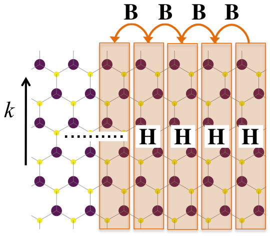
In an infinite system with translational symmetry between the layers, the strips are identical, and Eq. 1 becomes
| (2) |
with , , and for , see Fig. 1. For a left semi-infinite system with to , the equations remain the same, except for the equation, which becomes
| (3) |
In surface science the matrix block is called the surface Green’s function. In the context of 2D structures we call it the edge Green’s function.
In a similar way, for a right semi-infinite system with , only the equation for is different from the bulk equation, Eq. 2
| (4) |
with the matrix block the edge Green’s function. Note that if the 2D layer has no two-fold symmetry, such as inversion, a mirror plane perpendicular to the 2D layer, or a two-fold rotation axis perpendicular to the 2D layer, then , i.e., a right edge is different from a left edge.
The density of states of the edge strip of a left/right semi-infinite system is given by
| (5) |
where is the density of states projected on a single orbital .
Partitioning the infinite system into a right and a left semi-infinite halve, the on-strip matrix blocks of the Green’s function of the infinite system can be expressed as
| (6) |
II.1.1 Eigenmodes and Bloch matrices
We will express the Green’s function matrices of (semi)infinite systems in terms of Bloch matrices.Ando (1991) Equation 2 for is the same as the Schrödinger equation in tight-binding representation
| (7) |
where is the -dimensional vector of orbital coefficients of the wave function on strip . With translational symmetry between the strips, the elementary solution is a Bloch wave, and , with a complex constant. For an inifinite system this holds for all , and for a left (right) semi-infinite system for (). Using this relation as an ansatz in Eq. 7 gives a quadratic eigenvalue equation in of dimension .
| (8) |
As , if is a root of , then so is . Numerically, the solutions are usually found by solving an equivalent linear generalized eigenvalue equation of dimension ,Tisseur and Meerbergen (2001)
| (9) |
which resembles the eigenvalue equation for the transfer matrix.Lee and Joannopoulos (1981a, b); Hatsugai (1993); Hatsugai et al. (2006); Teo et al. (2008); Mong and Shivamoggi (2011)
The maximally solutions of this equation can be divided into two classes, i.e. right-going modes and left-going modes, labeled respectively by and superscripts in the following. Right-going modes are either evanescent waves that decay to the right, , or waves that travel to the right, meaning and a positive group velocity. Left-going modes either decay to the left, , or travel to the left, with negative group velocity. With the eigenvector belonging to the eigenvalue in Eq. 9, the group velocity is given byKhomyakov et al. (2005)
| (10) |
Only for traveling waves is the group velocity non-zero.
We divide the eigenvectors into a set of right-going modes and a set of left-going modes . The evanescent waves always come in pairs of a right-going and a left-going mode, i.e., if is the eigenvalue of a right-going mode, then gives a left-going solution. Traveling waves do not necessarily come in such pairs, and the numbers of right- and left-going traveling waves may be different. Neither right-going modes or left-going modes necessarily form a complete set in -dimensional space, nor are they an orthogonal set in general.
One can use these two sets of modes to form the two matrices
| (11) |
and construct the two Bloch matrices
| (12) |
where are the diagonal matrices with the eigenvalues on the diagonal, and are the (pseudo)inverses of .Golub and van Loan (1996) The Bloch matrices have the convenient property
| (13) |
for any integer , as , the identity matrix, with . It follows that
| (14) |
satisfies the tight-binding equation, Eq. 7, where set the boundary conditions in strip number 0. We assume that all relevant solutions can be expressed this way.
II.1.2 Green’s functions in terms of Bloch matrices
The general expression of Eq. 14 also applies to the columns of the Green’s function matrices, compare Eqs. 2 and 7. The boundary conditions require that a retarded Green’s function comprises traveling waves moving outwards from its point source and/or evanescent waves decaying away from the source. For left and right semi-infinite systems this gives
| (15) | |||||
| (16) |
Using Eq. 15 in Eqs. 2 and 3 then leads to
| (17) | |||
Solving these two equations gives the edge Green’s function of a left semi-infinite system as
| (18) |
where the inversion should be treated as a pseudoinversion if is singular.Golub and van Loan (1996) Using Eq. 16 in Eqs. 2 and 4 gives the edge Green’s function of a right semi-infinite system
| (19) |
Finally, using Eq. 6 gives the on-strip Green’s function matrix block of an infinite system
| (20) |
II.1.3 Ideal edge states
One cannot have traveling Bloch waves for energies in the band gap of a semiconductor. In semi-infite systems one can however have solutions in the form of evanescent states that originate from the edge of the system. One can find the energies of these edge states from the edge Green’s functions, Eqs. 18 and 19, which have isolated poles at these energies. Obviously in numerical calculations one has to work at complex energies to avoid these poles, but can be chosen small.
Alternatively, edge states can be obtained from the solutions of the eigenvalue problem, Eq. 8, solved at real energies .Lee and Joannopoulos (1981a); Harrison (2003); Teo et al. (2008); Dang et al. (2014) As edge states should decay away from the edge, only the modes can contribute to an edge state for a left semi-infinite system, and only the modes for a right semi-infinite system. An edge state of a left semi-infinite system has amplitude zero beyond the edge of that system, i.e., (Eq. 14). This means , the number of left-going solutions of Eq. 8. Because , see Eq. 12 with and , a necessary and sufficient condition for the existence of an edge state is that the eigenmodes are linearly dependent. A similar reasoning holds for the edge states of a right semi-infinite system. The number of edge states at a particular energy and wave number of a left/right semi-infinite system is then given by .
II.1.4 Ideal grain boundaries
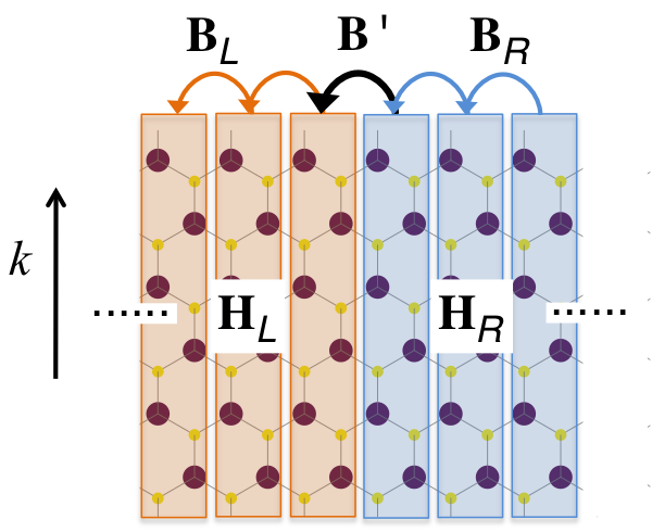
A model for an ideal grain boundary is shown in Fig. 2. Space is divided into two parts with the hopping matrix block connecting the left and right halves. We assume that the on-strip Hamiltonian matrix blocks of all the strips in the left half are given by right up to the boundary, and that the hopping matrix blocks between all nearest neighbor strips in the left part are given by . The corresponding matrix blocks for the right half are and , respectively. The Green’s function matrix blocks and pertaining to the two strips just left and right of the grain boundary interface can be derived like Eq. 6
| (21) | |||||
| (22) |
where and are the edge Green functions of the left and right semi-infinite systems, respectively. With Eqs. 18 and 19 one can express the interface Green’s functions in terms of Bloch matrices
| (23) | |||||
| (24) |
II.1.5 Modified edges
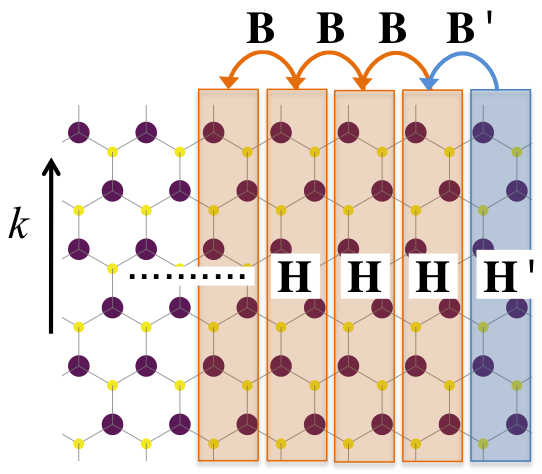
So far we have assumed that all layers are identical right up to an edge or grain boundary. The formation of an edge or boundary often involves an electronic and a structural reconstruction, which makes the Hamiltonian matrix blocks of the strips adjacent to an edge or grain boundary different from those of the bulk strips.
We illustrate this on a left semi-infinite system with an edge layer that is different from the bulk. The tight-binding equations for the two layers closest to the edge are
| (25) |
where is the on-site Hamiltonian of the edge layer, and is the coupling of this layer to the rest of the system, see Fig. 3. Using , see Eqs. 14 and 15, transforms Eq. II.1.5 into
| (26) |
In the terminology used in non-equilibrium Green’s function (NEGF) transport calculations, the term is called the self-energy of the left lead.Khomyakov et al. (2005) The Green’s function matrix blocks pertaining to the two layers closest to the edge are then given by
| (27) |
The Green’s function gives the density of states in the usual way, cf. Eq. 5. The density of states is zero for energies inside the band gap, except for isolated poles at particular energies, which represent the edge states of the modified edges. This formalism can be adapted in an obvious way to model modified edges of right semi-infinite systems, or grain boundaries where the strips left and right of the interface are modified.
II.1.6 Charge neutrality level
Experimentally the Fermi level in MX2 compounds is often determined by unintentional doping due to defects.Yong et al. (2008); McDonnell et al. (2014); KC et al. (2014) In addition, as MX2 compounds are polar materials, an internal electric field is created if a crystallite is terminated by polar edges.Güller et al. (2013); Gilbertini and Marzari (2015) Such an electric field can cause a long range charge transfer between different edges, even if the bulk material does not contain any impurities. The position of the Fermi level can then become dependent on the size and the shape of the sample, which makes the intrinsic Fermi level an ill-defined quantity.
Each edge or grain boundary has a well-defined energy level at which that edge or grain boundary is electrically neutral, the charge neutrality level (CNL). We use the CNL as a reference point in the following. The charge neutrality level is defined as the energy at which
| (28) |
where is the number of electrons that makes the strip neutral, and is the electron counting function
| (29) |
with is the -integrated density of states
| (30) |
The -resolved density of states can be obtained from Eq. 5 for edge strips, and a similar expression for a bulk strip.
II.2 MX2 edges
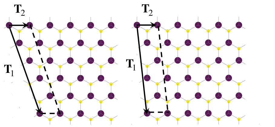
The hexagonal lattice of MX2 is shown in Fig. 4. We specify an edge starting from a supercell spanned by vectors and . This supercell is used to define a semi-infinite system, choosing one of the vectors as the translation vector parallel to the edge.
II.2.1 Zigzag and armchair edges
Similar to graphene the basic-type edges of the MX2 lattice are the zigzag and armchair edges as defined in Fig. 4. A zigzag edge is defined by and , with as the vector parallel to the edge. The matrix blocks discussed in section II.1 become
| (31) | |||||
| (32) |
where denotes the real space Hamiltonian matrix block that describes the interaction between atoms in the unit cell situated at the origin and atoms in the unit cell situated at . The matrix elements of depend on the specific tight-binding model that is used to represent the electronic structure of MX2. They are given in the appendices.
Note that by solving the quadratic eigenvalue equation, Eqs. 8 and 9, one has simultaneous access to the Green’s functions of the edges of a right and a left semi-infinite system via Eqs. 18 and 19. Unlike graphene the MX2 monolayer lacks inversion symmetry, which means that the zigzag edge termination of a right semi-infinite system is different from that of a left semi-infinite system, see Fig. 4. The zigzag edge of a right semi-infinite system is terminated by metal atoms. We call this the M-edge, consistent with previous studies on MoS2, where it is called the Mo-edge.Bollinger et al. (2001, 2003); Vojvodic et al. (2009) The zigzag edge of a left semi-infinite system is then called the X-edge, as it is terminated by chalcogen atoms. In previous studies on MoS2, it has been called the S-edge.
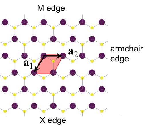
An edge in armchair orientationcan be constructed from and with the translation vector parallel to the edge, see Fig. 4. The corresponding supercell is twice as large as the unit cell, so the dimension of the matrix blocks defining the edge are twice the dimension of the blocks defining the zigzag edge.
| (33) |
| (34) |
Note that the termination at the edge is controlled by the contents of the cell used to define the primitive vectors . In particular, the cell defined in Fig. 4 does not lead to a pristine armchair edge, but one with additional M or X atoms attached to the edge. It is straightforward to remove these atoms and by applying the technique outlined in Sec. 3 obtain the electronic structure of a pristine armchair edge.
II.2.2 General edges
Edges with a somewhat more general orientation are defined by the supercell
| (35) |
with the translation vector parallel to the edge, defined as zigzag vectors plus armchair vectors, see Fig. 5. The angle with the direction of is given by
| (36) |
Because of the symmetry of the lattice one only has to cover the angle between a zigzag orientation , , and an armchair orientation , . Left and right edges (M-type and X-type edges) are then obtained by using and , respectively.
A series of edge orientations is obtained by setting and varying , where the translation vector along the edge is the sum of zigzag vectors and one armchair vector. We call this a generalized zigzag edge, see Fig. 5. The supercell defined by the lattice vectors, Eq. 35, contains unit cells. For instance, values give angles , respectively. The construction of the Hamiltonian matrix blocks defining the edge is straightforward. As an example, the Hamiltonian matrix blocks for , are
| (37) |
| (38) |
To generate edges with an orientation closer to the armchair edge () one can use the series with and vary . The translation vector parallel to the edge is then the sum of one zigzag vector and armchair vectors, which we call a generalized armchair edge, see Fig. 5. The supercell then contains unit cells. As an example, , gives . The edge termination can be controlled by adding and removing atoms at the edge, and apply the technique outlined in Sec. 3.
II.3 Tight-binding models
We consider tight-binding models with spin degeneracy, i.e., we neglect spin-orbit coupling. The main contributions to the valence and conduction bands of MX2 around the band gap come from the valence -shell of the M atom and the -shell of the X atoms. A minimal basis set then comprises eleven orbitals: five metal -orbitals, and six -orbitals of the two chalcogen atoms.Cappelluti et al. (2013) Monolayer MX2 has point-group symmetry. The trigonal prismatic coordination of the metal atom splits the d-states into three groups: {}, {}, and {}. The six -orbitals of the two chalcogen atoms split into the groups {}, {}, {} and {}. Mirror symmetry in the plane of the metal atoms, , allows for hybridization between orbitals that are even with respect to , i.e., and orbitals, or between orbitals that are odd, i.e., and orbitals.
The set of orbitals with even symmetry thus comprises the six orbitals , , , , , and , and the set with odd symmetry the five orbitals , , , , and . As the even/odd symmetry is conserved for the edges and grain boundaries considered in this paper, all corresponding Hamiltonian matrices are blocked, and the even/odd solutions can be obtained separately. The matrix blocks required for constructing the Hamiltonian matrices of Sec. II.2, are given in appendix B. The values of the tight-binding parameters have been obtained by fitting the bulk band structure to bands obtained from density functional theory (DFT) calculations with the generalized gradient approximation (GGA/PBE) functional.Perdew et al. (1996) For the even states we use the parameters given by Rostami et al.,Rostami et al. (2015) and for the odd states we use the parameters given in appendix B.
The eleven band model can be simplified further. From early theoretical studies and recent first-principles calculations one observes that the MX2 bands at the top of the valence band and at the bottom of the conduction band, are dominated by the metal d-orbitals, in particular those with even symmetry, i.e., , , and .Mattheiss (1973); Coehoorn et al. (1987); Cappelluti et al. (2013) Contributions to the bands around the gap from the and orbitals and from the chalcogen -orbitals are much smaller. Matheiss has constructed an effective tight-binding model for MX2, where only the metal sites are taken into account explicitly.Mattheiss (1973) These sites form a two-dimensional triangular lattice, and the presence of the X atoms lowers the symmetry of this lattice from to . The metal orbitals with even symmetry, , , and , are used to construct an effective three-band model. The matrix blocks of this model are given in appendix A. We use the parameters given by Liu et al.Liu et al. (2013), which have been obtained by fitting the bulk bands to GGA/PBE results.
III Results
III.1 Three-band model
III.1.1 Zigzag and armchair edges
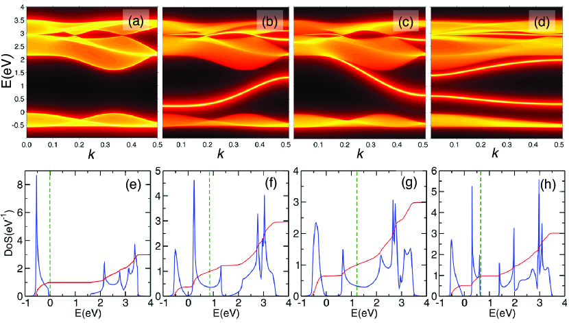
The eigenvalues and eigenvectors of Eq. 8, are used to construct the Bloch matrices, Eq. 12. The bulk density of states is shown in Fig. 6(a), as calculated from the Green’s function matrix of a bulk strip, Eqs. 2 and 20, in the zigzag edge orientation. In the three-band model, the lowest band is the valence band, and the overlapping two upper bands form the conduction band. Note that the zero of energy is chosen at the top of the valence band. The same Bloch matrices give access to the Green’s function matrices of the zigzag edge strips, Eqs. 18 and 19. Here and are the energy and -resolved Green’s function of the M-edge and the X-edge, respectively, see Fig. 4. Again using MoS2 as an example, the associated densities of state and of the Mo-edge, respectively the S-edge, are shown in Fig. 6(b) and (c).
The Mo-edge has a prominent edge state inside the bulk band gap dispersing upwards from to . The S-edge has an edge state that starts in the bulk conduction band at , and disperses downward to . In surface physics such states are termed Shockley states.Pershoguba and Yakovenko (2012) These edge states are also found in the more detailed eleven-band model with a similar dispersion, see Sec. III.2. The latter model shows a richer edge state structure, originating from bands that are omitted in the simple three-band model. Nevertheless, the three-band model finds prominent Mo-edge and the S-edge states with the correct dispersion. Edge states are also found at energies close to eV, which is in the hybridization gap between the two conduction bands.
The structure of a bulk strip in armchair orientation has a mirror plane perpendicular to the MX2-plane and along the armchair orientation, see see Fig. 4. It follows that the densities of states of right and left edges, and , are identical for the armchair orientation. The -resolved density of states of the MoS2 armchair edge, Eq. 33-34, is shown in Fig. 6(d). There are two clear edge states with energies in the band gap. One edge state is just below the conduction band and roughly follows the dispersion of the conduction band edge, whereas the other one is positioned at eV above the valence band, following the dispersion of valence band edge.
The -integrated densities of states, Eq. 30, of a bulk MoS2 strip in zigzag orientation, the Mo-edge, the S-edge, and the armchair edge, are given in Figs. 6(e)-(h), respectively. These densities of states show the van Hove singularities at the band edges that are typical of 1D structures. With the zero of energy at the top of the valence band, the bulk valence band lies in the energy range -0.0 eV, and the two conduction bands in the range 1.6-3.5 eV, see Fig. 6(e). The Mo-edge shows edge bands in the energy range 0.1-1.4 eV, and around 3 eV. The S-edge has an edge band starting at 0.5 eV, which merges with the conduction band at higher energies, and additional edge states with energies 2.7-3.0 eV. The armchair edge has two edge band in the gap at in the energy ranges 0.3-0.6 eV and 1.4-2.0 eV, respectively, and an edge state around 3.1 eV.
Also shown in Figs. 6(e)-(h) are the electron counting function (red curves), Eq. 29, and the charge neutrality level (CNL; green lines), Eq. 28. Obviously for the bulk the CNL is at the top of the valence band, see Fig. 6(e). The position of the CNL at the Mo-edge corresponds to a filled edge band in the gap, see Fig. 6(f). One might interpret this as effectively two-third of the bonds being broken for a Mo atom at the Mo-edge. Likewise, the position of the CNL at the S-edge corresponds to a filled edge band in the gap, see Fig. 6(g). This correlates with one-third of the bonds being broken for a Mo atom at the S-edge. The supercell of the armchair edge has two Mo atoms along the edge, where the local environments of one is similar to that of a Mo atom at an Mo-edge, and the local environment of the other is similar to that of a Mo atom at the S-edge, see Fig. 4. Summing the and edge state occupations at the Mo- and S-edges, one predicts that the armchair edge has one completely filled edge band. The calculated CNL shows that this is indeed the case; the armchair edge has one fully occupied edge band, and one empty edge band, see see Fig. 6(h).
The CNLs of all three basic edges are quite close, cf. Figs. 6(f)-(h). This is an artefact of the three-band model, and of disregarding the odd bands in particular. The latter play an important role in setting the CNLs in MX2 edges, as we will discuss in Sec III.2. In polar lattices such as MX2 the CNL does not fix the intrinsic Fermi level, unlike in a non-polar lattice such as graphene.Güller et al. (2013); Gilbertini and Marzari (2015) In a finite-sized MX2 sample electrons can be redistributed among all the edges in the sample, driven by the internal electric field set up by the intrinsic polarization of the material.
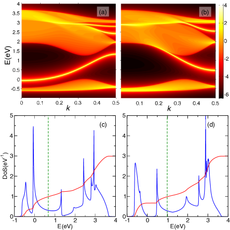
So far we have focused on edges of MoS2, but all MX2 compounds with a similar structure ( point group, trigonal prismatic coordination of M atoms by X atoms) have similar edge structures. Figure 7 shows the densities of states of the W and Te zigzag edges of -WTe2 as an example. These densities of states are very similar to those of the corresponding Mo- and S-edges of MoS2, see Figs. 6(b), (c), (f) and (g). The band gap of bulk WTe2 is somewhat smaller than that of MoS2, and the band widths are somewhat larger. WTe2 has a band gap of 1.1 eV (GGA/PBE), a valence band in the range -0.0 eV, and conduction bands in the range 1.1-3.7 eV. The W-edge has a state in the gap in the energy range 0.0-1.4 eV, and the Te-edge has a state in the gap in the range 0.5-2.0 eV. As is the case for the bulk bands, the band widths of these edge states are somewhat larger than the corresponding states in MoS2.
III.1.2 General edges and grain boundaries
The electronic structure of the more general edges defined in Sec. II.2.2 can be calculated along the same lines. Figs. 8(a) and (b) give the densities of states of generalized zigzag edges of MoS2 with translation vectors along the edge defined by and 3, respectively, and , see Eq. 35 and Fig. 5. The generalized zigzag edge has a rich structure of edge states within the bulk band gap. The peak at 0.4 eV in Figs. 8(a) and (b) results from the armchair part of this edge, compare to Fig. 6(h). The band in the range 1-1.5 eV in 8(a), and the structure of bands in the range 0.8-1.9 eV in 8(b) originates mainly from the zigzag parts.
The counting system for the three-band model, as outlined in the previous section, gives a filling 2/3 per Mo atom at a Mo-edge and a filling 1 per two Mo atoms at an armchair edge. For a generalized zigzag edge one would then predict the CNL to correspond to filled edge states. This would mean that the CNL is inside an edge band, unless is a multiple of three. This is confirmed by a calculation of the CNL according to Eq. 28. In Fig. 6(a), where , the position of the CNL corresponds to a 2/3-filled edge band, whereas in Fig. 6(b), where , the CNL is in a gap between two edge states. The gaps between the edge states of the general edges are quite small however. In a sample that involves long range charge transfer between the edges, as discussed above, these semiconducting edges easily become doped.
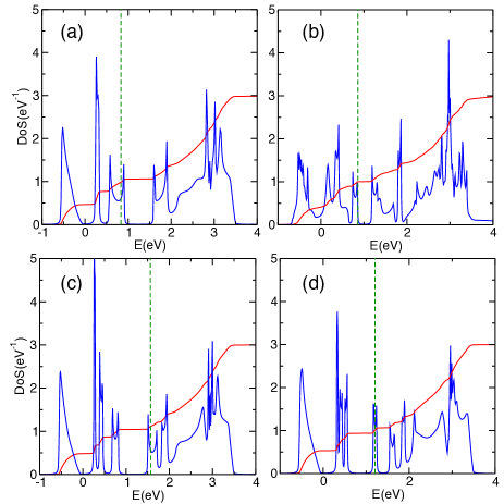
Figures 8(c)and (d) show the densities of states of generalized armchair edges of MoS2, with translation vectors along the edge with and and 3, respectively, see Eq. 35 and Fig. 5. Again this general edge has a rich structure of states within the bulk band gap. In particular the peaks around 0.4 eV and 1.7 eV have a strong armchair character. The counting model gives filled edge states, so it predicts that the CNL always lies inside an edge band. Calculations of the CNL according to Eq. 28 confirm this, as shown in Fig. 8(c) and (d). In conclusion, within the three-band tight-binding model, pristine charge neutral edges are metallic for most edge orientations.
A similar analysis can be applied to the states found at grain boundaries. We illustrate the use of Eq. 21 for calculating the states at grain boundaries using a simple grain boundary in MoS2. It consists of a left semi-infinite part, terminated by a S-edge, connected to a right semi-infinite part, terminated by a Mo-edge. As hopping matrix defining the coupling between left and right parts, Fig. 2, we choose a scaled version of the bulk hopping matrix, Eq. 32.
| (39) |
Obviously gives two uncoupled S- and Mo-edges with corresponding edge states, Figs. 6(b), (c), (f) and (g), whereas gives the bulk electronic structure, Figs. 6(a) and (e), without any edge states. The values then represent a simple model for a weak link with zigzag orientation.
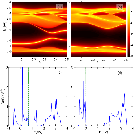
Figure 9(a) gives the -resolved density of states for , which represents a relatively weak coupling between the left and right parts. In the band gap one observes the two edge bands that are typical of the Mo-edge and the S-edge, see Figs. 6(b) and (c). Due to the coupling between the S- and Mo-edges at the grain boundary, the two bands interact, which results in an avoided crossing between the two edge states at and eV. The avoided crossing creates an energy gap in the range 0.7-1.2 eV, which is clearly visible in the -integrated density of states for , shown in Fig. 9(c). The counting model predicts 2/3, respectively 1/3 filling per Mo atom of an edge state at the Mo-edge and the S-edge, if the grain boundary is charge neutral. This implies that the lower edge band is fully occupied, whereas the upper edge band is empty. A calculation of the CNL according to Eq. 28 confirms this, see Fig. 9(c).
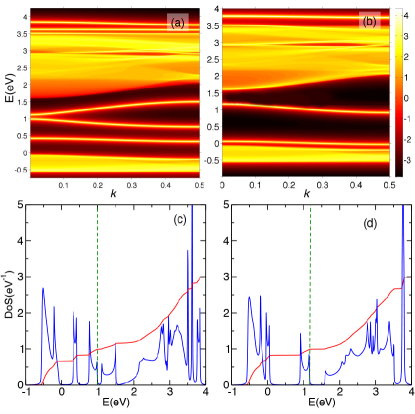
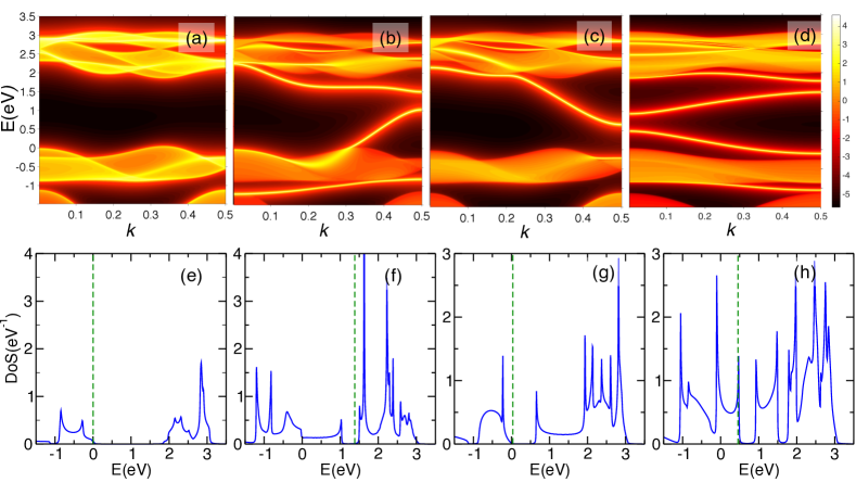
Figure 9(b) gives the -resolved density of states for a strong coupling between the left and right parts, . The interaction between the two edge bands is now much stronger than for the case discussed in the previous paragraph, which results in a much larger gap in the range 0.2-1.6 eV, see Fig. 9(d). The two edge bands are pushed toward the valence band and the conduction band, respectively, and they more closely follow the dispersions of the valence and conduction band edges. The occupancy of a charge neutral grain boundary is the same as before, i.e., a fully occupied lower edge band and an empty upper edge band.
As a final point in this section we illustrate the technique introduced in Sec. 3 for handling edges that involve an electronic or a structural reconstruction. For the zigzag edges we have found a 2/3 respectively a 1/3 occupied edge band for the Mo-edge and the S-edge. It suggests that a reconstruction that triples the translational period along the edge, may lead to fully occupied edge states for both edges. As a proof of principle, we test a very simple reconstruction, where one in three Mo atoms at the Mo-edge or the S-edge has a different on-site energy. The Green’s function matrix is calculated from Eq. II.1.5. The densities of states of the modified edge layers are shown in Fig. 10(a) and (c) for the Mo-edge and (b) and (d) for the S-edge. Obviously increasing the periodicity from to folds the edge band, so one observes three edge states instead of one. Decreasing the on-site energy of every third Mo atom at the edge by 1 eV introduces energy gaps between the edge states.
By calculating the CNL we observe that at the Mo-edge the two lowest edge bands, starting at 0.4 eV and 0.7 eV in Fig. 10(b) and (d), are filled, whereas the third band, starting at 1.1 eV, is empty. The lowest edge band of the S-edge at 0.0 eV, Fig. 10(a) and (c), is filled, whereas the two upper bands, starting at 0.9 eV and 1.6 eV, respectively, are empty.
III.2 Eleven-band tight-binding model
As discussed in Sec. II.3, the eleven-band tight-binding model of MX2 uses a basis set composed of the five valence -orbitals of the M atom, and the six valence orbitals of the two X atoms. Because mirror symmetry in the MX2 plane holds both for monolayers as well as for edges, states that are even or odd with respect this mirror symmetry are treated separately. The even symmetry set comprises the six orbitals , , , , , and , and the odd symmetry set the five orbitals , , , , and , leading to six- and five-dimensional Hamiltonian matrices, respectively.
Again we use MoS2 as an example of a MX2 monolayer. The procedure for obtaining the Green’s functions and the densities of states are the same as those described in the previous section. In the following we will only discuss the results obtained for the basic edges, the zigzag and the armchair edges, and compare those to the results obtained with the three-band model.
III.2.1 Even bands
The -resolved density of states of the even states of a bulk strip in the zigzag edge orientation is shown in Fig. 11(a) in an energy region around the band gap, and the corresponding -integrated density of states is given in Fig. 11(e). As before, the zero of energy is positioned at the top of the valence band. Qualitatively, these densities of states are similar to those of the three-band model, compare to Figs. 6(a) and (e). Quantitatively, the eleven-band model gives a highest valence band that is wider by eV, whereas the two lowest conduction bands are narrower by eV in total.
Figures 11(b) and (f) show the -resolved and -integrated densities of states of the Mo-edge. There are two prominent edge bands with energies in the MoS2 band gap. One edge band emerges from the bulk valence band at , and disperses upward with increasing to 1 eV. A second band disperses downward from the conduction band to 1.6 eV. The first edge band is also found in the three-band model, compare Figs. 6(b) and (f). In the three-band model it is found at a slightly higher energy, such that it is completely isolated from the bulk valence band. The second edge band is absent in the three-band model. We will discuss the character of these bands in more detail below. Like in the three-band model, there are also edge states at other energies, for instance just below the highest valence band at eV, and in the hybridization gaps of the conduction bands.
The -resolved and -integrated densities of states of the S-edge are given in Figs. 11(c) and (g). At energies in the MoS2 band gap there is one prominent edge state, which starts at in the conduction band, and disperses downward with increasing to 0.7 eV. The three-band model shows the same edge state with more or less the same dispersion, compare to Figs. 6(c) and (g). In the eleven-band model this state is somewhat more prominently isolated from the conduction band. Unlike for the Mo-edge, the eleven-band model does not give additional even edge states for the S-edge in the band gap, as compared to the three-band model.
Finally, Figs. 11(d) and (h) show the -resolved and -integrated densities of states of the armchair edge. There are three edge bands with energies in the MoS2 band gap. One band is situated at -0.5 eV and a second edge band lies at 0.9-1.5 eV. These two edge bands roughly correspond to the ones that are found in the three-band model of the armchair edge, see Figs. 6(d) and (h). In the eleven-band model these two edge bands are found at a slightly lower energy in the gap. In addition the present model finds a third edge band in the gap, just below the conduction band at 1.7-1.9 eV.
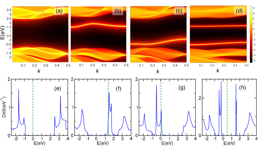
In conclusion, although there are quantitative differences between the electronic structures found with the eleven-band model and the three-band model, qualitatively they give similar results concerning the prominent edge states of even symmetry found in the MoS2 band gap. For the Mo-edge and the armchair edge, the eleven-band model gives an additional edge state, as compared to the three-band model, with energies just below the conduction band.
Figures 11(e)-(h) also show the CNLs. One needs of course all the bands to calculate the CNLs, including the odd bands to be discussed in the next section. A comparison to Fig. 6 reveals that the odd bands are in fact instrumental in fixing the CNLs. For instance, the CNLs of the Mo-edge and the S-edge differ by 1.4 eV, Figs. 11(f) and (g), whereas the corresponding CNLs in Figs. 6(f) and (g) differ by 0.3 eV only. The eleven-band model gives one completely occupied even edge band for the Mo-edge and one empty one, see Fig. 11(f). For the S-edge it gives one completely empty even edge band, see Fig. 11(g). This is unlike the the three-band model, where we found partially filled even edge bands, both for the Mo-edge and the S-edge. As we will see in the next section, edge states of odd symmetry, which are absent in the three-band model, pin the CNLs of the Mo-edge and the S-edge, and make these edges metallic. The CNL at the armchair edge is in the gap between the two edge bands, see Fig. 11(h), as it also is in the three-band model, see Fig. 6(h)
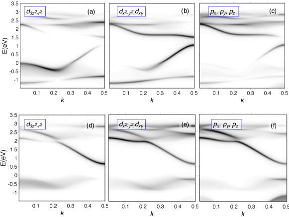
The orbital character of the edge states can be analyzed using the projected density of states, according to Eq. 5. The projections on the Mo orbital, the and orbitals, and the orbitals of the S atoms are given in Figs. 12(a), (b), and (c), respectively, for the Mo-edge. The results indicate that both edge states in the MoS2 band gap have a mixed Mo and S character. The dominant Mo contributions clearly come from the and orbitals. The upper edge state has S character mixed in, in particular for , whereas the lower edge state has some S character mixed in for . There is little character mixed in these edge bands, except at the band edges.
The projected densities of states of the S-edge, projected on the same orbitals, are given in Figs. 12(d), (e), and (f). Also here the edge state in the MoS2 band gap has a mixed Mo and S character. As for the Mo contribution, for the dominant character is Mo and . That changes somewhat for larger ; at the dominant character is Mo . The contribution of the S-orbitals is fairly constant throughout the whole edge band.
III.2.2 Odd bands
The -resolved and -integrated bulk densities of states corresponding to the odd states are given in Figs. 13(a) and (e). The band gap between the odd states is 3.3 eV, which is significantly larger than the gap between the even states. The top of the highest valence band of the odd states is approximately 0.8 eV below the top of the highest valence band of the even states, whereas the bottom of the lowest conduction band of the odd states is approximately 0.6 eV above that of the even states.
The -resolved densities of state of the odd bands are shown in Figs. 13(b) and (c) for the Mo-edge and of the S-edge, respectively, and the corresponding -integrated densities of states are shown in Figs. 13(f) and (g). Both edges have a prominent edge band with moderate dispersion inside the gap between the odd states. The edge band of the Mo-edge lies close to the conduction band between 1.3 and 1.8 eV, whereas the edge band of the S-edge is close to the top of the valence band between and 0.2 eV.
If we also take the bulk band structure of the even bands into consideration, Figs. 11(a) and (d), then most of the edge band at the S-edge, Figs. 13(c) and (g) overlaps with the valence band. It is still a true edge state though, because the interaction between the odd edge state and the even bulk bands is symmetry forbidden. The edge band at the Mo-edge, Figs. 13(b) and (f) partially overlaps with the conduction band of the even states. Also this is a true edge state over the whole 1D Brillouin zone, as interaction with the bulk states is symmetry forbidden.
Figures 13(d) and (h) give the -resolved and -integrated densities of states corresponding to the armchair edge. These results show two edge bands in the gap region with a modest to small dispersion. The lowest of these edge bands has a dispersion of 0.4 eV, and taking also the even bulk bands into consideration, it lies in the MoS2 valence band. The upper edge band is near dispersionless; it is found in the gap at 1.6 eV.
The calculated CNLs are also given in Figs. 13(e)-(h). From these figures it becomes clear that the odd edge states are instrumental in controlling the CNLs of the edges. The CNL of the Mo-edge is found in the edge band that is close to the MoS2 conduction band, see Fig. 13(f), and the CNL of the S-edge lies in the edge band close to the MoS2 valence band, see Fig. 13(g). Within the eleven-band model both these edges are metallic in their charge neutral state. The CNL of the armchair edge lies between the two edge bands, Fig. 13(h), which means that the neutral armchair edge is semiconducting.
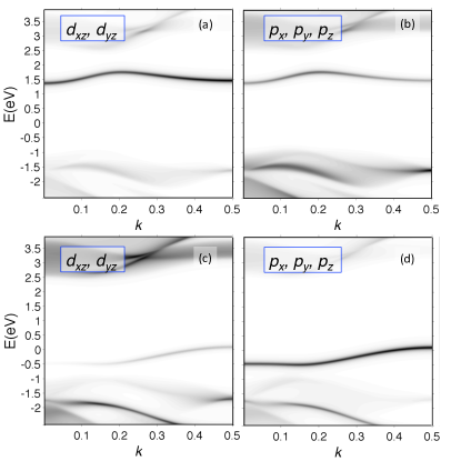
The orbital character of the odd symmetry edge states is identified using the projected densities of state. Figures 14(a) and (b) show the projections on the - and -orbitals of the density of states of the Mo-edge, and Figs. 14(c) and (d) show the projections for the S-edge. The edge state at the Mo-edge has somewhat of a mixed character, but it is dominated by Mo -orbitals. The edge state at the S-edge has a clear S character. More than the even edge states discussed in the previous section, these two odd edge states have a “dangling-bond” character, i.e., they correspond to bulk bonds that are broken at the edge atoms.
IV Summary and Conclusions
Growth of 2D semiconductors, such as the transition metal dichalcogenides MX2, commonly results in sheets that contain quasi-1D metallic structures, which are located at the edges of 2D crystallites, or at the boundaries between 2D crystal grains. Such edges and grain boundaries form a practical realization of 1D metals. Metalic edges have also been identified as the active sites in MX2 catalysts. A standard technique for modeling edge or grain boundary states starts from nanoribbon structures, which involves using large supercells if one aims at obtaining converged results that enable the separation between edge and bulk properties. Moreover, as a nanoribbon has two edges, electron transfer between the edges can occur in order to equilibrate the system, which complicates identifying the properties of single edges.
In this paper we formulate a Green’s function technique for calculating edge states of (semi-)infinite 2D systems with a single well-defined edge or grain boundary. We express bulk, edge and boundary Green’s functions in terms of Bloch matrices. The latter are constructed from the solutions of a quadratic eigenvalue equation, which gives the traveling and evanescent Bloch states of the system. Electronic and structural reconstructions of edges or grain boundaries are easily incorporated in the technique. The formalism can be implemented in any localized basis set representation of the Hamiltonian.
Here we use it to calculate edge and grain boundary states of MX2 monolayers by means of tight-binding models. A simple three-band model is employed to explore the electronic structures of the basic pristine zigzag and armchair edges in MX2. Within this model the zigzag edges are metallic in their charge neutral state, whereas the armchair edge is semiconducting. The three-band model is also used to analyze the electronic structures of MoS2 edges with a more general orientation between zigzag and armchair; these edges are generally metallic. The same model is applied to obtain electronic structures of grain boundaries and of structurally modifed edges.
The three-band model captures only part of MX2 edge electronic structure. A more complete picture of the rich electronic structure of MX2 edges is obtained from an eleven-band tight-binding model comprising the metal valence orbitals and the valence orbitals of the chalcogen atoms. Edge states in the band gap with even symmetry (with respect to a mirror through the plane of M atoms) are qualitatively similar to those found in the three-band model. As in the latter model, charge neutral zigzag edges are metallic and the armchair edge is semiconducting in the eleven-band model. Unlike the three-band model, however, the charge neutrality level is fixed by edge states of odd symmetry in the band gap. The odd states have a character that reflects the dangling bonds on the edge atoms, unlike the even states, which have more of a mixed M- and X- character. The odd edge states are likely to be found near the Fermi level under experimental conditions, and can not be discarded when modeling MX2 edges.
Acknowledgements.
This work is part of the research program of the Foundation for Fundamental Research on Matter (FOM), which is part of the Netherlands Organization for Scientific Research (NWO).Appendix A Three-band tight-binding model
Following Mattheis, the three-band tight binding model discussed in Sec II.3 only explicitly uses the sublattice of the M atoms and the -orbitals of and symmetry, i.e., the orbitals that are symmetric with respect to , mirror symmetry in the MoS2 plane.Mattheiss (1973) We number these orbitals as
| (40) |
The matrix blocks discussed in Sec. II.2 are then matrices, where denotes the real space Hamiltonian matrix block pertaining to the interaction between atoms in the unit cell at the origin and atoms in the unit cell at . Using only nearest neighbor interactions, one has . Defining the tight-binding parameters and , and making use of the rotation properties of the -orbitals, one derives the matrix blocks
| (41) |
| (42) |
The hopping associated with matrix elements is even with respect to inversion and the one associated with is odd. It is then easy to see that
| (43) |
The values of the tight-binding parameters are taken from Liu et al.,Liu et al. (2013) which have been ontained by fitting the tight-binding band structure of a MX2 sheet to a DFT GGA/PBE band structure,Perdew et al. (1996) using the highest valence band and the two lowest conduction bands in the fit. GGA/PBE gives an optimized lattice parameter of Å for MoS2, which is 1-2 % larger than the reported experimental values.Young (1968); Al-Hilli and Evans (1972); Böker et al. (2001) With this lattice parameter the calculated band gap is 1.63 eV, which is smaller than the experimental optical band gap of 1.85 eV.Mak et al. (2010)
Appendix B Eleven-band tight-binding model
The eleven-band tight-binding model of MX2 uses a basis set composed of all five -orbitals of the M atom, and the six orbitals of the two X atoms. Following the approach of Cappelluti et al.,Cappelluti et al. (2013); Castellanos-Gomez et al. (2013) we include next nearest neighbor interactions, and use the Slater-Koster two-center approximation for the hopping matrix elements.Slater and Koster (1954) The real space matrix blocks discussed in Sec. II.2 then have the form
| (44) |
with the remaining blocks constructed according to Eq. 43. The bulk Hamiltonian for an infinite layer with two-dimensional translation symmetry is written in this notation as
| (45) |
The parameters in the model can be found by fitting the tight-binding band structure obtained with this bulk Hamiltonian to a band structure obtained from a DFT calculation. The model turns out to be too restrictive to obtain a satisfactory fit for all eleven bands with one parameter set. A good fit can however be obtained if we divide the bands into a set of even symmetry, and a set of odd symmetry, and use different parameters for the two sets. Mirror symmetry in the MX2 plane holds for monolayers, as well as for edges, so states that are even or odd with respect to , can be treated separately. In Sec. B.1 we give the expressions for the matrix blocks and in Eq. 44 for the even states, and in Sec. B.2 for the odd states.
B.1 Even states
The even states are composed of orbitals of and symmetry,
| (46) |
The matrix blocks and in Eq. 44 are then all
| (47) |
where are the on-site orbital energies and are the Slater-Koster two-center integrals.Slater and Koster (1954) Similarly,
| (48) |
| (49) |
| (50) |
| (51) |
| (52) |
| (53) |
| (54) |
We use values of the parameters as obtained by Rostami at al. from fitting the even tight-binding bands to DFT GGA/PBE bands.Rostami et al. (2015) A lattice parameter of Å for MoS2 has been used in these calculations, which is 1% smaller than the optimized GGA/PBE value, but close to the reported experimental values. It results in a calculated band gap of 1.76 eV, which is slightly smaller than the experimental optical band gap of 1.85 eV.Mak et al. (2010) We have shifted the tight-binding bands such, that the zero of energy coincides with the top of the valence band.
B.2 Odd states
The odd states are composed of orbitals of and symmetry,
| (55) |
The matrix blocks in Eq. 44 are if and if , whereas the matrix blocks are are if , if , and if
| (56) |
| (57) |
| (58) |
| (59) |
| (60) |
| (61) |
| (62) |
We obtain values of the parameters by fitting the tight-binding bands of odd symmetry to bands obtained from a density functional theory (DFT) calculation with the generalized gradient GGA/PBE functional,Perdew et al. (1996); Kresse and Furthmüller (1996); Kresse and Joubert (1999) using the same lattice parameter as for the even bands. The optimal parameters are given in table 1, and the quality of the fit can be judged from Fig. 15.

References
- Geim and Novoselov (2007) A. K. Geim and K. S. Novoselov, Nat. Mater. 6, 183 (2007).
- Xu et al. (2013) M. Xu, T. Liang, M. Shi, and H. Chen, Chem. Rev. 113, 3766 (2013).
- Geim and Grigorieva (2013) A. K. Geim and I. V. Grigorieva, Nature 499, 419 (2013).
- Chhowalla et al. (2013) M. Chhowalla, H. S. Shin, G. Eda, L.-J. Li, K. P. Loh, and H. Zhang, Nat. Chem. 5, 263Ð275 (2013).
- Helveg et al. (2000) S. Helveg, J. V. Lauritsen, E. Lægsgaard, I. Stensgaard, J. K. Nørskov, B. S. Clausen, H. Topsøe, and F. Besenbacher, Phys. Rev. Lett. 84, 951 (2000).
- Ci et al. (2010) L. Ci, L. Song, C. Jin, D. Jariwala, D. Wu, Y. Li, A. Srivastava, Z. F. Wang, K. Storr, L. Balicas, F. Liu, and P. M. Ajayan, Nat. Mater. 9, 430 (2010).
- Levendorf et al. (2012) M. P. Levendorf, C.-J. Kim, L. Brown, P. Y. Huang, R. W. Havener, D. A. Muller, and J. Park, Nature 488, 627 (2012).
- van der Zande et al. (2013) A. M. van der Zande, P. Y. Huang, D. A. Chenet, T. C. Berkelbach, Y. You, G.-H. Lee, T. F. Heinz, D. R. Reichman, D. A. Muller, and J. C. Hone, Nat. Mater. 12, 554 (2013).
- Najmaei et al. (2013) S. Najmaei, Z. Liu, W. Zhou, X. Zou, G. Shi, S. Lei, B. I. Yakobson, J.-C. Idrobo, P. M. Ajayan, and J. Lou, Nat. Mater. 12, 754 (2013).
- Liu et al. (2014) H. Liu, L. Jiao, F. Yang, Y. Cai, X. Wu, W. Ho, C. Gao, J. Jia, N. Wang, H. Fan, W. Yao, and M. Xie, Phys. Rev. Lett. 113, 066105 (2014).
- Li et al. (2015) M.-Y. Li, Y. Shi, C.-C. Cheng, L.-S. Lu, Y.-C. Lin, H.-L. Tang, M.-L. Tsai, C.-W. Chu, K.-H. Wei, J.-H. He, W.-H. Chang, K. Suenaga, and L.-J. Li, Science 349, 524 (2015).
- Son et al. (2006) Y.-W. Son, M. L. Cohen, and S. G. Louie, Nature 444, 347 (2006).
- Yazyev and Katsnelson (2008) O. V. Yazyev and M. I. Katsnelson, Phys. Rev. Lett. 100, 047209 (2008).
- Bollinger et al. (2001) M. V. Bollinger, J. V. Lauritsen, K. W. Jacobsen, J. K. Nørskov, S. Helveg, and F. Besenbacher, Phys. Rev. Lett. 87, 196803 (2001).
- Bollinger et al. (2003) M. V. Bollinger, K. W. Jacobsen, and J. K. Nørskov, Phys. Rev. B 67, 085410 (2003).
- Vojvodic et al. (2009) A. Vojvodic, B. Hinnemann, and J. K. Nørskov, Phys. Rev. B 80, 125416 (2009).
- Botello-Méndez et al. (2009) A. R. Botello-Méndez, F. López-Urías, M. Terrones, and H. Terrones, Nanotechnology 20, 325703 (2009).
- Andersen et al. (2014) K. Andersen, K. W. Jacobsen, and K. S. Thygesen, Phys. Rev. B 90, 161410 (2014).
- Zou et al. (2013) X. Zou, Y. Liu, and B. I. Yakobson, Nano Lett. 13, 253 (2013).
- Zhou et al. (2013) W. Zhou, X. Zou, S. Najmaei, Z. Liu, Y. Shi, J. Kong, J. Lou, P. M. Ajayan, B. I. Yakobson, and J.-C. Idrobo, Nano Lett. 13, 2615 (2013).
- Giamarchi (2003) T. Giamarchi, Quantum Physics in One Dimension (Oxford University Press, Oxford, 2003).
- Schweiger et al. (2002) H. Schweiger, P. Raybaud, G. Kresse, and H. Toulhoat, J. Catal. 207, 76 (2002).
- Nakada et al. (1996) K. Nakada, M. Fujita, G. Dresselhaus, and M. S. Dresselhaus, Phys. Rev. B 54, 17954 (1996).
- Akhmerov and Beenakker (2008) A. R. Akhmerov and C. W. J. Beenakker, Phys. Rev. B 77, 085423 (2008).
- Delplace et al. (2011) P. Delplace, D. Ullmo, and G. Montambaux, Phys. Rev. B 84, 195452 (2011).
- Ataca et al. (2011) C. Ataca, H. Şahin, E. Aktürk, and S. Ciraci, J. Phys. Chem. C 115, 3934 (2011).
- Wang et al. (2010) Z. Wang, H. Li, Z. Liu, Z. Shi, J. Lu, K. Suenaga, S.-K. Joung, T. Okazaki, Z. Gu, J. Zhou, Z. Gao, G. Li, S. Sanvito, E. Wang, and S. Iijima, J. Am. Chem. Soc. 132, 13840 (2010).
- Kou et al. (2012) L. Kou, C. Tang, Y. Zhang, T. Heine, C. Chen, and T. Frauenheim, J. Phys. Chem. Lett. 3, 2934 (2012).
- Seivane et al. (2013) L. F. Seivane, H. Barron, S. Botti, M. A. Lopes Marques, Á. Rubio, and X. López-Lozano, J. Mater. Res. 28, 240 (2013).
- Çakır and Peeters (2014) D. Çakır and F. M. Peeters, Phys. Rev. B 89, 245403 (2014).
- Chu et al. (2014) R.-L. Chu, G.-B. Liu, W. Yao, X. Xu, D. Xiao, and C. Zhang, Phys. Rev. B 89, 155317 (2014).
- Xu et al. (2014) G. Xu, J. Wang, B. Yan, and X.-L. Qi, Phys. Rev. B 90, 100505 (2014).
- Lucking et al. (2015) M. C. Lucking, J. Bang, H. Terrones, Y.-Y. Sun, and S. Zhang, Chem. Mater. 27, 3326 (2015).
- Pavlović and Peeters (2015) S. Pavlović and F. M. Peeters, Phys. Rev. B 91, 155410 (2015).
- Bernholc and Pantelides (1978) J. Bernholc and S. T. Pantelides, Phys. Rev. B 18, 1780 (1978).
- Pollmann and Pantelides (1978) J. Pollmann and S. T. Pantelides, Phys. Rev. B 18, 5524 (1978).
- Lee and Joannopoulos (1981a) D. H. Lee and J. D. Joannopoulos, Phys. Rev. B 23, 4988 (1981a).
- Lee and Joannopoulos (1981b) D. H. Lee and J. D. Joannopoulos, Phys. Rev. B 23, 4997 (1981b).
- Chang and Schulman (1982) Y.-C. Chang and J. N. Schulman, Phys. Rev. B 25, 3975 (1982).
- Ando (1991) T. Ando, Phys. Rev. B 44, 8017 (1991).
- Khomyakov and Brocks (2004) P. A. Khomyakov and G. Brocks, Phys. Rev. B 70, 195402 (2004).
- Khomyakov et al. (2005) P. A. Khomyakov, G. Brocks, V. Karpan, M. Zwierzycki, and P. J. Kelly, Phys. Rev. B 72, 035450 (2005).
- Khomyakov and Brocks (2006) P. A. Khomyakov and G. Brocks, Phys. Rev. B 74, 165416 (2006).
- Zwierzycki et al. (2008) M. Zwierzycki, P. A. Khomyakov, A. A. Starikov, K. Xia, M. Talanana, P. X. Xu, V. M. Karpan, I. Marushchenko, I. Turek, G. E. W. Bauer, G. Brocks, and P. J. Kelly, Phys. Status. Solidi. B 245, 623 (2008).
- Tisseur and Meerbergen (2001) F. Tisseur and K. Meerbergen, SIAM Rev. 43, 235 (2001).
- Mattheiss (1973) L. F. Mattheiss, Phys. Rev. B 8, 3719 (1973).
- Liu et al. (2013) G.-B. Liu, W.-Y. Shan, Y. Yao, W. Yao, and D. Xiao, Phys. Rev. B 88, 085433 (2013).
- Cappelluti et al. (2013) E. Cappelluti, R. Roldán, J. A. Silva-Guillén, P. Ordejón, and F. Guinea, Phys. Rev. B 88, 075409 (2013).
- Hatsugai (1993) Y. Hatsugai, Phys. Rev. Lett. 71, 3697 (1993).
- Hatsugai et al. (2006) Y. Hatsugai, T. Fukui, and H. Aoki, Phys. Rev. B 74, 205414 (2006).
- Teo et al. (2008) J. C. Y. Teo, L. Fu, and C. L. Kane, Phys. Rev. B 78, 045426 (2008).
- Mong and Shivamoggi (2011) R. S. K. Mong and V. Shivamoggi, Phys. Rev. B 83, 125109 (2011).
- Golub and van Loan (1996) G. Golub and C. F. van Loan, Matrix Computations (Johns Hopkins University Press, Baltimore, 1996).
- Harrison (2003) W. A. Harrison, Phys. Scripta. 67, 253 (2003).
- Dang et al. (2014) X. Dang, J. D. Burton, A. Kalitsov, J. P. Velev, and E. Y. Tsymbal, Phys. Rev. B 90, 155307 (2014).
- Yong et al. (2008) K. S. Yong, D. M. Otalvaro, I. Duchemin, M. Saeys, and C. Joachim, Phys. Rev. B 77, 205429 (2008).
- McDonnell et al. (2014) S. McDonnell, R. Addou, C. Buie, R. M. Wallace, and C. L. Hinkle, ACS Nano 8, 2880 (2014).
- KC et al. (2014) S. KC, R. C. Longo, R. Addou, R. M. Wallace, and K. Cho, Nanotechnology 25, 375703 (2014).
- Güller et al. (2013) F. Güller, A. M. Llois, J. Goniakowski, and C. Noguera, Phys. Rev. B 87, 205423 (2013).
- Gilbertini and Marzari (2015) M. Gilbertini and N. Marzari, Nano Lett. 15, 6229 (2015).
- Perdew et al. (1996) J. P. Perdew, K. Burke, and M. Ernzerhof, Phys. Rev. Lett. 77, 3865 (1996).
- Rostami et al. (2015) H. Rostami, R. Roldán, E. Cappelluti, R. Asgari, and F. Guinea, Phys. Rev. B 92, 195402 (2015).
- Coehoorn et al. (1987) R. Coehoorn, C. Haas, J. Dijkstra, C. J. F. Flipse, R. A. de Groot, and A. Wold, Phys. Rev. B 35, 6195 (1987).
- Pershoguba and Yakovenko (2012) S. S. Pershoguba and V. M. Yakovenko, Phys. Rev. B 86, 075304 (2012).
- Young (1968) P. A. Young, J. Phys. D Appl. Phys. 1, 936 (1968).
- Al-Hilli and Evans (1972) A. Al-Hilli and B. Evans, J. Cryst. Growth 15, 93 (1972).
- Böker et al. (2001) T. Böker, R. Severin, A. Müller, C. Janowitz, R. Manzke, D. Voß, P. Krüger, A. Mazur, and J. Pollmann, Phys. Rev. B 64, 235305 (2001).
- Mak et al. (2010) K. F. Mak, C. Lee, J. Hone, J. Shan, and T. F. Heinz, Phys. Rev. Lett. 105, 136805 (2010).
- Castellanos-Gomez et al. (2013) A. Castellanos-Gomez, R. Roldán, E. Cappelluti, M. Buscema, F. Guinea, H. S. J. van der Zant, and G. A. Steele, Nano Letters 13, 5361 (2013).
- Slater and Koster (1954) J. C. Slater and G. F. Koster, Phys. Rev. 94, 1498 (1954).
- Kresse and Furthmüller (1996) G. Kresse and J. Furthmüller, Phys. Rev. B 54, 11169 (1996).
- Kresse and Joubert (1999) G. Kresse and D. Joubert, Phys. Rev. B 59, 1758 (1999).