Mg(OH)2-WS2 Heterobilayer: Electric Field Tunable Bandgap Crossover
Abstract
Magnesium hydroxide (Mg(OH)2) has a layered brucite-like structure in its bulk form and was recently isolated as a new member of 2D monolayer materials. We investigated the electronic and optical properties of monolayer crystals of Mg(OH)2 and WS2 and their possible heterobilayer structure by means of first principles calculations. It was found that both monolayers of Mg(OH)2 and WS2 are direct-gap semiconductors and these two monolayers form a typical van der Waals heterostructure with a weak interlayer interaction and a type-II band alignment with a staggered gap that spatially seperates electrons and holes. We also showed that an out-of-plane electric field induces a transition from a staggered to a straddling type heterojunction. Moreover, by solving the Bethe-Salpeter equation on top of single shot G0W0 calculations, we show that the oscillator strength of the intralayer excitons of the heterostructure is an order of magnitude larger than the oscillator strength of the interlayer excitons. Because of the staggered interfacial gap and the field-tunable energy band structure, the Mg(OH)2-WS2 heterobilayer can become an important candidate for various optoelectronic device applications in nanoscale.
pacs:
31.15.A, 31.15.E, 68.35.bg, 78.67-nI Introduction
Over the past decade, graphene, a two dimensional form of carbon atoms arranged in a honeycomb structure, led to an enormous interest in the field of two dimensional materials due to its exceptional physical propertiesNovo1 ; Geim1 . However, the lack of a band gap is a major obstacle for the use of graphene in optoelectronic applications. Subsequently other novel two dimensional (2D) materials such as hexagonal structures of III-V binary compoundsNovo3 ; hasan1 and transition metal dichalcogenides (TMDs)Gordon ; Wang have gained a lot of interest due to their wide range of band gap energies. The synthesized members of TMDs, notably MoS2Radisavlijevic , MoSe2Lu , WS2Matte , and recently ReS2Tongay and ReSe2Wolverson which have band gaps around 1-2 eV, are suitable monolayer materials for many optoelectronic applications. Beyond being novel atomic-thick materials, lateral and vertical heterostructures of these monolayer crystals have also recieved considerable attention.
As constituents of possible heterostructures TMDs are very promissing. Those new members of 2D monolayer materials have tunable electronic properties from metalic to wide-gap semiconductingWilson ; Ataca and excellent mechanical propertiesGomez . Moreover, TMDs can be used in various fields such as nanoelectronicsRadisavlijevic ; Li ; Popov , photonicsEda ; Mak ; Yin , and for transistorsWang , catalysisDrescher , hydrogen storageSeayad , and Li-ion battery applicationsChang . Among TMDs, WS2 has been studied intensively. It is an indirect-gap semiconductor in its bulk form while it shows a transition to direct-gap character in its monolayer formBoker ; Klein ; Thomalla . It was shown by Ramasubramaniam that the optoelectronic properties of WS2 and MoX2 (X=S or Se) monolayers are tunable through quantum confinement of carriers within the monolayersRamasubramaniam . Shi et al. showed that the electron effective mass decreases as the applied strain increases, and monolayer WS2 possesses the lightest charge carriers among the TMDsShi . In addition, strong excitonic features of WS2, including neutral and redshifted charged excitons were observed by Mak et al.Mak2 Due to these interesting electronic and optical properties, one may go a step further and construct 2D heterostructures incorporating monolayer WS2 with other 2D monolayer with the potential to achieve enhanced functionalities.
Recently synthesized monolayer of Mg(OH)2, a member of alkaline-earth hydroxides (AEH), with formula X(OH)2 where X = Mg or Ca, are candidate materials for constructing such heterostructures. Magnesium and calcium hydroxides are multifunctional materials which have many important applications in industry, technology, solid-state electronics, and in photovoltaic devicesEstrela ; Ghali ; Cao ; Snider . Recently, we studied Ca(OH)2 monolayer crystals and found that the number of layers of Ca(OH)2 does not affect the electronic, structural, and magnetic properties qualitatively while the intrinsic mechanical stiffness of each layer becomes slightly larger as the structure changes from monolayer to bilayer. Very recently, Torun et al.Torun investigated the electronic and optical properties of the heterobilayer structure GaS-Ca(OH)2 and found that it is a type-II heterojunction where spatially seperated charge carriers can be formed. The optical spectra of different stacking types exhibit distinct properties. Like Ca(OH)2, Mg(OH)2 has a layered structure in its bulk form possessing the trigonal symmetry of the space group Pm1 (brucite)Desgranges ; Catti ; Busing . Mg(OH)2 itself is a wide-gap insulator with a band gap of 7.6 eV found experimentally for the bulk structureMurakami . Kuji et al. reported properties of C-doped Mg(OH)2 films and found that the material becomes transparent in the visible region and electrically conducting which are favourable properties for applications in photovoltaic devicesKuji . Huang et al.Huang found experimentally a spectral peak near the band edge corresponding to strongly localized excitons with an exciton binding energy of 0.53 eV. This indicates a strong localization of the hole and electron to the oxygen px and py states. Most recently, successful synthesis of Mg(OH)2 monolayers on MoS2 and their optical properties were reported by Suslu et al.Suslu
Here, we predict an electric field dependence of the electronic and optical properties of the Mg(OH)2-WS2 heterobilayer structure. Our results reveal that monolayer crystal of Mg(OH)2 combined with TMDs may lead to the emergence of novel multifunctional nanoscale optoelectronic devices.
The paper is organized as follows: Details of the computational methodology is given in Sec. II. Structural and electronic properties of monolayers of Mg(OH)2 and WS2 are presented in Sec. III while the structural properties of the Mg(OH)2-WS2 heterobilayer are presented in Sec. IV. The effect of an external electric field on the electronic properties of the heterobilayer structure is given in Sec. V. In Sec. VI the electric field dependence of the optical properties of the heterobilayer are disscussed. Finally, we conclude in Sec. VII.
II Computational Methodology
For our first-principles calculations, we employed the plane-wave basis projector augmented wave (PAW) method in the framework of density-functional theory (DFT). For the exchange-correlation potential, the generalized gradient approximation (GGA) in the Perdew- Burke-Ernzerhof (PBE) formGGA-PBE1 ; GGA-PBE2 was employed as implemented in the Vienna ab-initio Simulation Package (VASP)vasp1 ; vasp2 . The van der Waals (vdW) correction to the GGA functional was included by using the DFT-D2 method of GrimmeGrimme . The inherent underestimation of the band gap given by DFT within the inclusion of spin-orbit-coupling (SOC) is corrected by using the Heyd-Scuseria-Ernzerhof (HSE) screened-nonlocal-exchange functional of the generalized Kohn-Sham schemeHeyd . Analysis of the charge transfers in the structures was determined by the Bader techniqueHenkelman .
The dielectric function and the optical oscillator strength of the individual monolayers and the heterostructure were calculated by solving the Bethe-Salpeter equation (BSE) on top of single shot GW (G0W0) calculation which was performed over standard DFT calculations including spin-orbit coupling (SOC). During this process we used -centered k-point sampling. The cutoff for the response function was set to 200 eV. The number of bands used in our calculations is 320. The cutoff energy for the plane-waves was chosen to be 400 eV. We included 4 valence and 4 conduction bands into the calculations in the BSE step.
The energy cut-off value for the plane wave basis set was taken to be eV. The total energy was minimized until the energy variation in successive steps became less than eV in the structural relaxation and the convergence criterion for the Hellmann-Feynman forces was taken to be eV/Å. The minimum energy was obtained by varying the lattice constant and the pressure was reduced below 1 kbar. 27271 -centered k-point sampling is used for the primitive unit cell. The Gaussian broadening for the density of states calculation was taken to be 0.05. In order to investigate the effect of an external electric field, an electric field is applied in the direction normal to the plane of the heterobilayer. The binding energy per unit cell was calculated by using the following formula: =+-, where and denote the total energies of WS2 and Mg(OH)2 monolayers, respectively, while denotes the total energy of the heterobilayer structure.
| Geometry | Magnetic | |||||||||||||
|---|---|---|---|---|---|---|---|---|---|---|---|---|---|---|
| (Å) | (Å) | (Å) | (Å) | (Å) | State | () | (meV) | (eV) | (eV) | (eV) | (eV) | |||
| Mg(OH)2 | 1T | 3.13 | 3.13 | 2.09 | 0.96 | - | NM | 2.9 | - | 3.25 | 3.22 | 4.75 | 4.15 | |
| WS2 | 1H | 3.18 | 3.18 | - | - | 2.41 | NM | 1.1 | - | 1.86 | 1.54 | 2.30 | 5.29 | |
| Heterobilayer | 1T | 3.16 | 3.16 | 2.10 | 0.96 | 2.41 | NM | - | 147 | 1.05 | 0.97 | 2.24 | 4.34 |
III single layer Mg(OH)2 and WS2
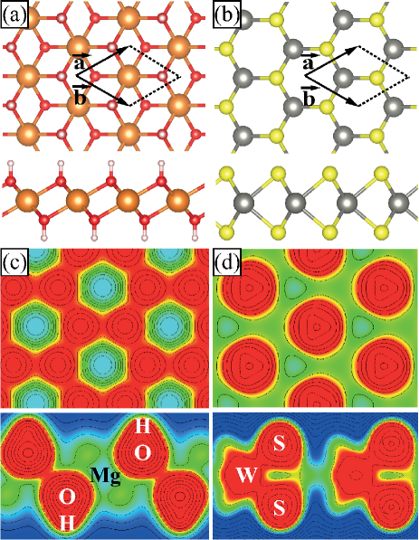
Monolayer Mg(OH)2 consists of hydroxyl (OH) groups bonded to Mg atoms. As seen in Fig. 1, the layer of Mg atoms is sandwiched between the OH groups in which O and H atoms are strongly bonded to each other. The calculated lattice parameters for monolayer Mg(OH)2 are ==3.13 Å. The thickness of monolayer Mg(OH)2 is 4.01 Å. The bond length of Mg-O and O-H bonds are calculated to be 2.09 Å and 0.96 Å, respectively. Bader charge analysis shows that ionic bond character is present in the Mg(OH)2 monolayer. In the structure each H atom donates 0.6 to neighboring O atom and each Mg donates 0.85 per O atom.
Generic forms of monolayer structures of TMDs display honeycomb lattice symmetry with the 1H phase for the dichalcogenides of Mo and W atoms. The calculated lattice parameters for the 1H phase of WS2 monolayer are ==3.18 Å which is very close to that of Mg(OH)2 monolayer. The W-S bond length in WS2 is calculated to be 2.42 Å. The thickness of the layer is 3.13 Å which is thinner than monolayer Mg(OH)2. In the monolayer WS2 0.55 of charge accumulation occurs from a W atom to each of the S atoms and the corresponding bonding character is covalent.
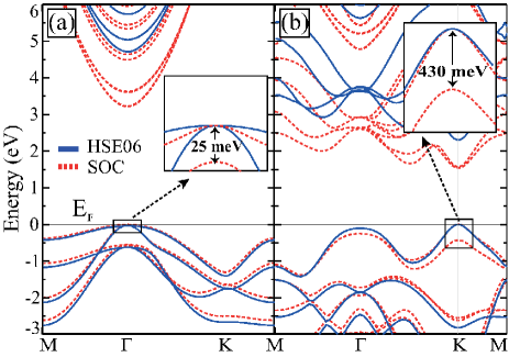
The calculated band structures within HSE06 correction are shown in Fig. 2. Monolayer Mg(OH)2 is found to be a direct band gap semiconductor with a band gap of 4.75 eV. Both the valence band maximum (VBM) and the conduction band minimum (CBM) reside at the point in the Brillouin zone (BZ). The states in the VBM of the Mg(OH)2 monolayer are composed of and orbitals of the O atoms.
Similar to the monolayer Mg(OH)2, monolayer WS2 is also a direct band gap semiconductor but with a lower band gap of 2.30 eV. As in other TMDs, both the VBM and CBM of single layer WS2 lie at the K point in the BZ. As seen in Fig. 2(b), spin-orbit interaction at the VBM states is much stronger since the states are composed of and orbitals of W atoms. There is an energy splitting of 430 meV at VBM which is much larger than that of monolayer Mg(OH)2 which is calculated to be 25 meV.
IV Heterobilayer
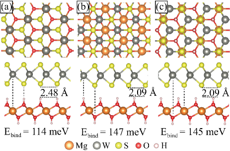
The calculated lattice constants of Mg(OH)2 and WS2 monolayers are very close to each other and therefore it is possible to construct a heterostructure of these monolayers where we may assume a primitive unit cell containing 8 atoms in total. We considered three different high-symmetry stacking configurations of the monolayers (see Fig. 3). We found that two of the stacking configurations have binding energies very close to each other but the one with the W atoms residing on top of an interface OH group is the ground state with a binding energy of 147 meV. For the lowest energy stacking configuration the interlayer distance is calculated to be 2.09 Å and the individual atomic bond lengths remain the same as in their isolated layers. The analysis for the charge transfers between the individual layers demonstrate that there is no depletion from one layer to the other for all the stacking geometries shown in Fig. 3. This result is expected due to the weak vdW interaction between the individual layers.
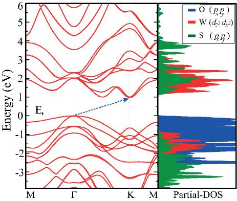
The calculated energy-band structure for the heterobilayer displays a semiconducting character with an indirect band gap of 2.24 eV. As seen in Fig. 4, the VBM of the heterobilayer that originates from the Mg(OH)2 layer lies at the point while the CBM of the structure which arises from the WS2 layer lies at the K point. Calculated energy-band diagram of the heterostructure also indicates the weak interlayer interaction. As seen in Fig. 4, the partial DOS (PDOS) indicates that the VBM of heterobilayer exclusively consists of and orbitals of the O atoms while the CBM is characterized by the orbitals of W and S atoms. This also demonstrates the type-II nature of the heterojunction: the two band edges originate from different individual layers and consequently the excited electrons and holes are confined in different layers which leads to the formation of spatially indirect excitons.
V Effect of External Electric Field
Applying an external electric field is one of the common method to modify or tune the physical properties of materials. In the field of 2D materials, a perpendicular electric field can lead to doping and in the case of bilayers it can induce charge transfer between layers. Castro et al. reported that the electronic band gap of a graphene bilayer structure can be controlled externally by applying a gate bias. They showed that the band gap changes from zero to midinfrared energies for field values 1 V/nmCastro . Chu et al. showed a continuous bandgap tuning in bilayer MoS2 with applied gate voltageChu . Here we present our results for the effect of a perpendicular electric field on the electronic and optical properties of the heterobilayer.
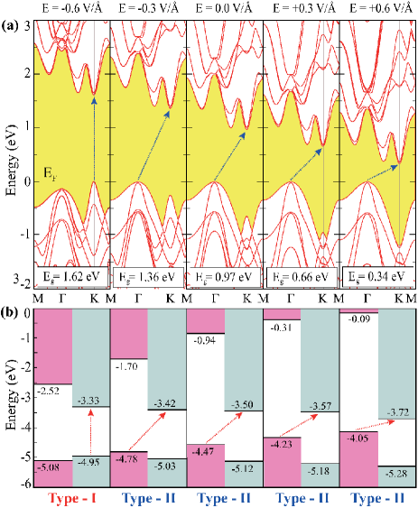
As seen in Fig. 5(a), the heterostructure is an indirect band gap semiconductor when there is no external electric field, in which the VBM is at but the CBM is at the K point. Appyling a positive electric field decreases the band gap (from 0.97 eV to 0.34 eV for E= +0.6 V/Å). The reason for such decreasing band gap is the shift of the band edges at the and the K points. Increasing the value of the positive electric field shifts the VBM of Mg(OH)2 up in energy while it shifts the CBM of WS2 down resulting in a decrease of the energy gap. The indirect character of the energy gap is not affected by the field. However, changing the direction of the applied electric field widens the band gap and ultimately leads to an indirect-to-direct band-gap-crossover as seen in Fig. 5(a).
When the strength of the electric field is -0.6 V/Å, it is clearly seen that both VBM and CBM of the heterobilayer reside at the K high symmetry point in the BZ. Thus, a transition from staggered gap to a straddling gap (type-I heterojunction) occured as shown in Fig. 5 (b). In fact, the critical electric field value for which this indirect-to-direct band-gap-crossover occurs is calculated to be 0.51 V/Å. At this critical value of the applied electric field, the valence band edge energy of the bands at the and K points become degenerate. As seen in Fig. 5(a), the bands at the valence band edge of the K point, which originate from the WS2 layer, shift up while the bands at the point which originate from the Mg(OH)2 layer shift down when making the external electric field more negative. Due to these opposite shifts of the VBM of the individual layers (see Fig. 5(b)) a transition from indirect-to-direct gap is predicted at a certain value of the applied field. After the transition to type-I heterojunction both type of charge carriers are confined to the WS2 layer which is desirable for applications in optoelectronic devices and for semiconductor laser applications. It is also important to point out that including quasiparticle energies might slightly change the band gap and the electric field value for which the indirect-to-direct band-gap-crossover occurs. However, the overall tunability characteristic of the heterobilayer using electric field would remain the same.
VI OPTICAL PROPERTIES
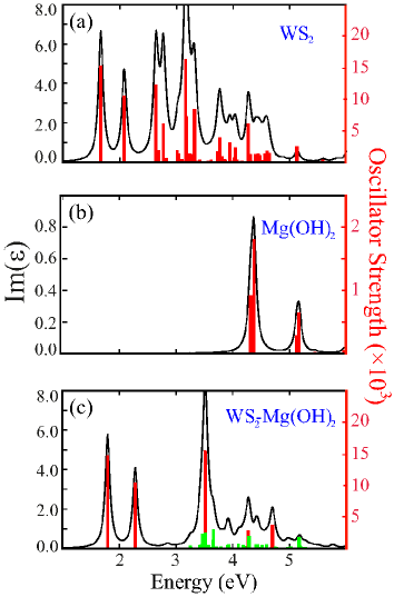
In order to investigate the optical properties of the isolated monolayers and the heterostructure, we solved the BSE equation on top of G0W0 calculation. In Fig. 6 we show the imaginary part of the dielectric function and the oscillator strength of the optical transitions of WS2 (Fig. 6(a)), Mg(OH)2 (Fig. 6(b)) and WS2-Mg(OH)2 heterostructure (Fig. 6(c)).
The first two peaks at 1.67 and 2.08 eV in the optical spectrum of monolayer WS2 (Fig. 6(a)) originate from the optical transitions at the K point in the BZ. The splitting (410 meV) of these two peaks is consistent with the splitting of the VBM bands at the K point due to the SOC effect (Fig. 2). Our calculations show that the oscillator strength of the optical transitions of the WS2 monolayer is an order of magnitude larger than that of the Mg(OH)2 monolayer. The first two optical transitions for the monolayer Mg(OH)2 (Fig. 6(b)) are split with a very small energy of 58 meV, this value is close to the value of the VBM splitting at the point due to the SOC effect (Fig. 2).
In Fig. 6(c) we show the imaginary part of the dielectric function and the oscillator strength of the optical transitions of the WS2-Mg(OH)2 heterostructure. As seen from the figure the first two peaks in the optical spectrum originate from the WS2 monolayer. The splitting of the first two peaks increases to 480 meV and the positions of them are blueshifted due to the interaction between the two monolayers. Although the oscillator strength of the peaks from the Mg(OH)2 monolayer are small, they can still be identified around 4 eV in the optical spectrum. The exciton binding energy of WS2, Mg(OH)2 and the heterobilayer is found to be as 0.84 eV, 2.4 eV and 0.74 eV, respectively.
As discussed earlier, the WS2-Mg(OH)2 heterostructure is a type-II heterojunction in the absence of an electric field. In this kind of heterojunctions spatially direct absorption (intralayer excitons) and spatially indirect emission (intralayer excitons) are expected as observed experimentally in the WSe2-MoS2 heterostructure. fangpnas Therefore, different exciton peaks might dominate the optical spectrum depending on the measurement method. For instance, the intralayer excitons (red optical transitions in Fig. 6(c)) will dominate the absorption spectrum, while interlayer excitons (green optical transitions in Fig. 6(c)) dominate the emission spectrum (i.e. photoluminescence (PL) measurements) of the heterostructure. So, in order to make a reasonable comparison between experiment and our calculations, we identified the optical transitions that correspond to inter- and intralayer excitons and plot them, respectively, in green and red color in Fig. 6(c). As shown in Fig. 6(c), the main optical transitions of the heterostructure originate from the intralayer recombinations and their oscillator strength is an order of magnitude larger than the oscillator strength of the interlayer excitons.
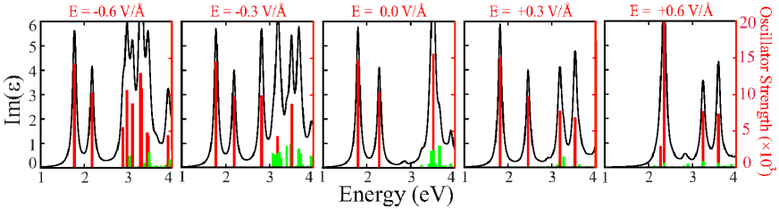
As mentioned before, the WS2-Mg(OH)2 heterobilayer has a type-II alignment and it transforms into a type-I heterostructure under an external out-of-plane electric field of -0.51 V/Å. In order to investigate the variation in the optical properties of the heterobilayer under different electric field strengths, we calculated the dielectric function and the oscillator strength of the different optical transitions under out-of-plane electric field of -0.6, -0.3, 0 , 0.3 and 0.6 V/Å which are shown in Fig. 7. Since the WS2-Mg(OH)2 heterobilayer remains type-II for out-of-plane electric field of -0.3, 0 , 0.3 and 0.6 V/Å, the red optical transitions will dominate the absorption spectrum but the green ones dominate the PL measurements. When the external out-of-plane electric field is -0.6 V/Å, the structure becomes type-I. In this case, the intralayer optical transitions (red) will dominate the PL measurements. Therefore, we predict an increase in the PL intensity of the WS2-Mg(OH)2 heterobilayer when the out-of-plane electric field becomes more negative than -0.51 V/Å. Applying perpendicular electric field also modifies the exciton binding energy of the heterobilayer. According to our calculations, the exciton binding energy of the heterobilayer becomes 0.77, 0.76, 0.65 and 0.10 eV for -0.6, -0.3, 0.3 and 0.6 V/Å electric field, respectively.
VII Conclusion
We investigated the structural, electronic and optical properties of the monolayers Mg(OH)2 and WS2 and its heterobilayer structure. In addition the effect of an applied out-of-plane electric field on the electronic and optical properties of the heterobilayer were investigated. We found that both Mg(OH)2 and WS2 are direct-gap semiconductors while the Mg(OH)2-WS2 heterobilayer structure is an indirect-gap semiconductor. Our results demonstrated that both the band gap and the energy-band dispersion of the heterobilayer structure can be tuned by the application of an external perpendicular electric field. At an applied electric field of -0.51 V/Å a transition from a staggered to a straddling gap heterojunction occurs which can be used for optoelectronic and semiconductor laser applications. In addition, by solving the Bethe-Salpeter equation on top of single shot G0W0 calculations, we predict that the oscillator strength of the intralayer excitons of the heterostructure is an order of magnitude larger than the oscillator strength of the interlayer excitons. It appears that heterobilayers of TMDs and AEHs may find applications in various nanoscale optoelectronic devices.
Acknowledgements.
This work was supported by the Flemish Science Foundation (FWO-Vl) and the Methusalem foundation of the Flemish government. Computational resources were provided by TUBITAK ULAKBIM, High Performance and Grid Computing Center (TR-Grid e-Infrastructure). H.S. is supported by a FWO Pegasus Long Marie Curie Fellowship. H.S. and R.T.S. acknowledge the support from TUBITAK through project 114F397.References
- (1) —————————————–
- (2) K. S. Novoselov, A. K. Geim, S. V. Morozov, D. Jiang, Y. Zhang, S. V. Dubonos, I. V. Grigorieva, and A. A. Firsov, Science 306, 666 (2004).
- (3) K. S. Novoselov, A. K. Geim, S. V. Morozov, D. Jiang, M. I. Katsnelson, I. V. Grigorieva, S. V. Dubonos, and A. A. Firsov, Nature (London) 438, 197 (2005).
- (4) K. S. Novoselov, D. Jiang, F. Schedin, T. Booth, V. V. Khotkevich, S. Morozov, and A. K. Geim, Proc. Natl. Acad. Sci. U.S.A. 102, 10451 (2005).
- (5) H. Sahin, S. Cahangirov, M. Topsakal, E. Bekaroglu, E. Akturk, R. T. Senger, and S. Ciraci, Phys. Rev. B 80, 155453 (2009).
- (6) R. A. Gordon, D. Yang, E. D. Crozier, D. T. Jiang, and R. F. Frindt, Phys. Rev. B 65, 125407 (2002)
- (7) Q. H. Wang, K. K. Zadeh, A. Kis, J. N. Coleman, and M. S. Strano, Nat. Nanotech. 7, 699 (2012).
- (8) B. Radisavljevic, A. Radenovic, J. Brivio, V. Giacometti, and A. Kis, Nat. Nanotech. 6, 147 (2011).
- (9) X. Lu, M. I. B. Utama, J. Lin, X. Gong, J. Zhang, Y. Zhao, S. T. Pantelides, J. Wang, Z. Dong, Z. Liu, W. Zhou, and Q. Xiong, Nano Lett. 14, 2419 (2014).
- (10) H. S. S. R. Matte, A. Gomathi, A. K. Manna, D. J. Late, R. Datta, S. K. Pati, and C. N. R. Rao, Angew. Chem., Int. Ed. 49, 4059 (2010).
- (11) S. Tongay, H. Sahin, C. Ko, A. Luce, W. Fan, K. Liu, J. Zhou, Y. S. Huang, C. H. Ho, J. Y. Yan, D. F. Ogletree, S. Aloni, J. Ji, S. S. Li, J. B. Li, F. M. Peeters, and J. Q. Wu, Nat. Commun. 5, 3252 (2014).
- (12) D. Wolverson, S. Crampin, A. S. Kazemi, A. Ilie, and S. J. Bending, ACS Nano 8, 11154 (2014).
- (13) J. Wilson and A Yoffe, Adv. Phys. 18, 193 (1969).
- (14) C. Ataca, H. Sahin, and S. Ciraci, J. Phys. Chem. C 116, 8983 (2012)
- (15) A. C. Gomez, M. Poot, G. A. Steele, H. S. J. van der Zant, N. Agrait, and G. R. Bollinger, Adv. Mater. 24, 772 (2012).
- (16) H. Li, Z. Yin, Q. He, H. Li, X. Huang, G. Lu, D.W.H. Fam, A.I.Y. Tok, Q. Zhang, and H. Zhang, Small 8, 63 (2012).
- (17) I. Popov, G. Seifert, and D. Tomanek, Phys. Rev. Lett. 108, 156802 (2012)
- (18) G. Eda, H. Yamaguchi, D. Voiry, T. Fujita, and M. Chen, Nano Lett. 11, 5111 (2011).
- (19) K. F. Mak, C. Lee, J. Hone, J. Shan, and T. F. Heinz, Phys. Rev. Lett. 105, 136805 (2010).
- (20) Z. Yin, H. Li, H. Li, L. Jiang, Y. Shi, Y. Sun, G. Lu, Q. Zhang, and X. Chen, H. Zhang, ACS Nano 6, 74 (2012)
- (21) T. Drescher, F. Niefind, and W. Bensch, W. Grunert, J. Am. Chem. Soc. 134, 18896 (2012).
- (22) A. M. Seayad and D. M. Antonelli, Adv. Mater. 16, 765 (2004).
- (23) K. Chang and W. X. Chen, ACS Nano 5, 4720 (2011).
- (24) T. Boker, R. Severin, A. Muller, C. Janowitz, R. Manzke, D. Voss, P. Kruger, A. Mazur, and J. Pollmann, Phys. Rev. B 64, 235305 (2001).
- (25) A. Klein, S. Tiefenbacher, V. Eyert, C. Pettenkofer, and W. Jaegermann, Phys. Rev. B 64, 205416 (2001).
- (26) M. Thomalla and H. Tributsch, J. Phys. Chem. B 110, 12167 (2006).
- (27) A. Ramasubramaniam, Phys. Rev. B 86, 115409 (2012).
- (28) H. Shi, H. Pan, Y. W. Zhang, and B. I. Yakobson, Phys. Rev. B 87, 155304 (2013).
- (29) K. F. Mak, K. He, C. Lee, G. H. Lee, J. Hone, T. F. Heinz, and J. T. Shan, Nat. Mater. 12, 207 (2013).
- (30) C. Estrela, F. C. Pimenta, I. Y. Ito, and L. L. Bammann, J. Endod. 24, 15 (1998).
- (31) Q. Cao, F. Huang, Z. Zhuang, and Z. Lin, Nanoscale 4, 2423 (2012).
- (32) E. Ghali, W. Dietzel, and K. U. Kainer, J. Mater. Eng. Perform. 13, 7 (2004).
- (33) A. C. Snider, Mat. Res. Soc. Symp. Proc. 757, 1 (2003).
- (34) E. Torun, H. Sahin, and F. M. Peeters, Phys. Rev. B 93, 075111 (2016).
- (35) L. Desgranges, G. Calvarin, and G. Chevrier, Acta Crystallogr. 52, 82 (1996).
- (36) M. Catti, G. Ferraris, S. Hull, and A. Pavese, Phys. Chem. Miner. 22, 200 (1995).
- (37) W. R. Busing and H. A. Levy, J. Chem. Phys. 26, 563 (1957).
- (38) T. Murakami, T. Honjo, and T. Kuji, Mater. Trans. 52, 1689 (2011).
- (39) T. Kuji, M. Chiba, T. Honjo, and K. Kotoda, J. Chem. Phys. 26, 563 (1957).
- (40) C. H. Huang, Y. L. Jan, and W. C. Lee, J. Electrochem. Soc. 45, 2618 (2006).
- (41) A. Suslu, K. Wu, H. Sahin, B. Chen, S. Yang, H. Cai, T. Aoki, S. Horzum, J. Kang, F. M. Peeters, and S. Tongay, Sci. Reports, 6, 20525 (2016).
- (42) J. P. Perdew, K. Burke, and M. Ernzerhof, Phys. Rev. Lett. 77, 3865 (1996).
- (43) J. P. Perdew, K. Burke, and M. Ernzerhof, Phys. Rev. Lett. 78, 1396 (1997).
- (44) G. Kresse and J. Hafner, Phys. Rev. B 47, 558 (1993).
- (45) G. Kresse and J. Hafner, Phys. Rev. B 49, 14251 (1994).
- (46) S. J. Grimme, Comput. Chem. 27, 1787 (2006).
- (47) J. Heyd, G. E. Scuseria, and M. Ernzerhof, J. Chem. Phys. 118, 8207 (2003).
- (48) G. Henkelman, A. Arnaldsson, and H. Jonsson, Comput. Mater. Sci. 36, 354 (2006).
- (49) H. Fanga, C. Battagliaa, C. Carraroc, H. A. Bechtelg, G. K. Palssonb, M. C. Marting, R. Maboudianc, S. B. Desaia, F. Kronasth, and Ali Javeya, PNAS 111, 6198 (2014).
- (50) E. V. Castro, K. S. Novoselov, S. V. Morozov, N. M. R. Peres, J. M. B. Lopes dos Santos, J. Nilsson, F. Guinea, A. K. Geim, and A. H. Castro Neto, Phys. Rev. Lett. 99, 216802 (2007).
- (51) T. Chu, H. Ilatikhameneh, G. Klimeck, R. Rahman, and Z. Chen, Nano Lett. 15, 8000 (2015).