Transferable tight binding model for strained group IV and III-V materials and heterostructures
Abstract
It is critical to capture the effect due to strain and material interface for device level transistor modeling. We introduced a transferable sp3d5s* tight binding model with nearest neighbor interactions for arbitrarily strained group IV and III-V materials. The tight binding model is parameterized with respect to Hybrid functional(HSE06) calculations for varieties of strained systems. The tight binding calculations of ultra small superlattices formed by group IV and group III-V materials show good agreement with the corresponding HSE06 calculations. The application of tight binding model to superlattices demonstrates that transferable tight binding model with nearest neighbor interactions can be obtained for group IV and III-V materials.
I Introduction
Modern field effect transistors have reached critical device dimensions in sub-10 nanometer. To surpass the coming limits of downscaling of field effect transistor, innovative devices such as tunneling field-effect transistors(TFET) Choi et al. (2007); Appenzeller et al. (2004); Zhang et al. (2008) and superlattice field-effect transistors Gnani et al. (2011); Long et al. (2014) are actively investigated. Those devices rely strongly on the usage of hetero-structures and strain techniques. To have reliable prediction of the performance in those devices, it is critical to have a atomistic model that is able to model strained ultra-small heterostructures accurately.
Ab-initio methods offer atomistic representations with subatomic resolution for a variety of materials and heterostructures. However, accurate ab-initio methods, such as Hybrid functionalsHeyd et al. (2006); Krukau et al. (2006), GWHedin (1965); Hybertsen and Louie (1986) and BSEIsmail-Beigi and Louie (2003) approximations are in general computationally too expensive to be applied to systems with a size of realistic device. Furthermore, those methods assume equilibrium and cannot truly model out-of-equilibrium device conditions where e.g. a large voltage might have been applied to drive carriers. For these reasons, more efficient semi-empirical approaches, such as the Bahder (1990); Tan et al. (2008); Huang et al. (2013), the empirical pseudopotentialFischetti and Laux (1996) and the empirical tight-binding(ETB) methodsJancu et al. (1998); Boykin et al. (2002); Tan et al. (2015) are actively developed.
Among these empirical approaches, ETB method has established itself as the standard state-of-the-art basis for realistic device simulationsFonseca et al. (2013). ETB has been successfully applied to electronic structures of millions of atoms Klimeck et al. (2002) as well as on non-equilibrium transport problems that even involve inelastic scattering Lake et al. (1993). For strained systems, modified ETB models take into account the altered environment in terms of both bond angle and length. In the simplest tight binding strain model, generalized Harrison’s lawHarrison (1999); Jancu et al. (1998); Tserbak et al. (1993) is usually adopted to describe bond-length dependence of the nearest-neighbor coupling parameters. Changes of bond angles in interatomic interactions are automatically incorporated through the Slater-Koster formulasPodolskiy and Vogl (2004). This simplest tight binding strain model can reproduce some hydrostatic and uniaxial deformation potentialsJancu et al. (1998), while much higher accuracy can be achieved by introducing the strain-dependent onsite parameters. Boykin et al. Boykin et al. (2002) introduced nearest neighbor position dependent diagonal orbital energies to the sp3d5s* tight binding model to reproduce correct deformations under [001] strains. Off-diagonal onsite corrections are suggested by Niquet et al. Niquet et al. (2009) and Boykin et al.Boykin et al. (2010) to model the strain behavior of indirect conduction valleys of materials with diamond structures under [110] strains.
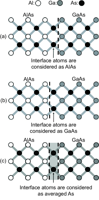
Those existing ETB strain models are fitted to pure strained bulk material instead of more complicated nanostructures. However, the transferability of those ETB models and parameters is questionable when applied to heterostructures. First of all, traditional ETB parameters depend on material types, while material type around interfaces can not be clearly defined. Fig.1 shows three possible definitions of materials near a GaAs/AlAs interface. Interface As atoms are interpreted as atoms in either (a) As of AlAs or (b) As of GaAs. Another usual assumption, shown by definition (c),is to take the interface As atoms to have an average of the onsite potentials. All those definitions are customarily used but with no hard data to justify. Secondly, it was shown that ETB parameters obtained by direct fitting possibly lead to unphysical results in nano-structures like ultra-thin bodiesTan et al. (2015, 2013). To improve the transferability of ETB parameters, ab-initio mapping methods are developed in ref Tan et al., 2015. This method is an ab-initio wave functions based tight binding parameterization algorithm. With this method, it is shown that ETB models are transferable to Si and GaAs ultra thin bodies.
In this paper, a new ETB model for strained materials considering only nearest neighbor interactions is introduced for strained group IV and III-V semiconductors. This strain model takes account of arbitrary strain effects to band structure. Transferable ETB parameters for strained III-Vs and group IV materials are obtained by ab-initio mapping algorithm from Hybrid functional calculations. The ETB model shows good transferability when applied to strained superlattices.
This paper is organized as follows. In section II, the ETB model for strained materials is described. Section III shows the validation of the ETB model for strained systems and superlattices. Subsection III.2 describes the details of getting ETB parameters; ETB parameters for strained group IV and III-V materials are listed in this section. Subsection III.3 compares the tight binding and hybrid functional results for unstrained and strained materials. Subsection III.4 presents the application of ETB model in strained superlattices, the tight binding results for superlattices are compared with hybrid functional calculations. Finally, the ETB model of strained materials and corresponding results are summarized in Section IV.
II Model
The ETB model of strained materials in this work is based on the multipole expansionEdmonds (1976) of the local potential near each atom. This ETB model has environment dependency, and it does not rely on the selection of coordinates. It can be applied to arbitrarily strained and rotated systems. In this work, the tight binding model is applied to group IV and III-V semiconductors which have diamond or zincblende structures. However, the application of this model is in principle not limited to group IV and III-V semiconductors. For materials considered in this work, the interaction range considered in the tight binding model is limited to the first nearest neighbors. In the following sections, letters in bold such as and are used for three dimensional vectors; correspondingly, and are used to denote the lengths of and . stands for polar angle and and azimuth angle of a three dimensional vector. , and correspond to tuples of angular and magnetic quantum numbers , and of ETB orbitals respectively. Dirac notation is used for ETB basis functions, e.g. stands for orbital of atom .
|
|
|
|
|
|
|
|
|
|
|
|
|
|
|
|
|
|
|
|
|
|
|
|
|
|
|
|
|
|
|
|
|
|
|
II.1 Multipole expansion of atomic potentials
The local potential near atom is approximated by a summation of the potential of atom and potential of its nearest neighbors(NNs)
| (1) |
where the relative position between atoms and is . The potential at contributed by atom at is approximated by generalized spherical potential. This generalized spherical potential centered at has multipole expansion given by
| (2) |
where and stands for angles and of vectors and . The is the radial part of multipole potential with angular momentum . By substituting in eq (1) by equation (2), the total potential near atom given by equation (1) can be written as a summation of multipole potentials
| (3) |
where the multipole potentials ’s are given by
| (4) | |||||
The ’s are summations of multipoles over nearest neighbors. The strain induced multipole potentials up to quadrupole (with ) are considered in this work. The describes the crystal potential under hydrostatic strain. depends only bond lengths. For unstrained or hydrostatically strained zincblende and diamond structures, both dipole potential and quadrupole potential are zero due to the crystal symmetry of zincblende and diamond structures. For strained systems with traceless diagonal strain component like , is induced due to angle change; while for strained systems with off-diagonal strain component like , both and are induced.
II.2 Strain dependent tight binding Hamiltonian
The strain dependent ETB Hamiltonian is constructed according to the multipole expansion of . Similar to the multipole expansion of the total potential given by eq (3), the strain dependent ETB Hamiltonian is written as
| (5) |
where the depends on multipole potential . Matrix element is thus written as .
II.3 Onsite elements
The has contribution from atom and its neighbors. Similar to , the diagonal onsite energies also has contribution from atom and contributions from its neighbors. The contribution of neighbors to diagonal onsites energies is separated to orbital dependent part and orbital independent part . The onsite elements due to is given by
| (6) |
with
| (7) | |||||
| (8) |
Here the is the reference bond length. In this work, the bond length of unstrained GaAs is chosen as . The parameter is introduced to modulate discrepancy between ab-initio results and experimental results. Non-zero ’s are introduced to match the ETB results in this work with experimental data under room temperature; while with zero , ETB results match the zero temperature ab-initio results. The term depends on orbital and atom type instead of material type. The summation over and are the environment dependent part of diagonal onsite energies . is used to modulate the band offset and it satisfies . Similar expression is also applied to spin-orbit coupling terms . In this work, only spin-orbit interaction of p orbitals is considered, and the bond length dependency of is neglected.
Due to dipole and quadrupole potentials, non-zero off-diagonal onsite elements appear. Off-diagonal onsite elements due to multipole potentials are given by
| (9) |
Since the given by eq (4) is non-spherical, to estimate these terms, following relation is used
| (10) |
where the is the Gaunt coefficient Gaunt (1929) defined by
| (11) |
with .
With eq (4), off-diagonal onsite elements of atom can be written as a summation of terms depending on atom and its neighbors
| (12) |
where the is the integral of radial parts of , and , given by
| (13) |
The is given by
| (14) |
The explicit form of ’s due to multipole potentials are given by appendix A.
The strained onsite model by equation (12) is essentially equivalent to the Slater Koster relations which was also used by Niquet et al Niquet et al. (2009) and Boykin et al Boykin et al. (2010). Onsite energies in Niquet’s work depend on strains components linearly; while Boykin’s onsite model uses Harrison’s law. Differently from those previous works, the diagonal onsite energies in this work follow an exponential dependency of bond lengths, and the off-diagonal onsite energies depend on symmetry breaking strains linearly which are described by equation (12). It should be noted that, for unstrained zincblende and diamond structures, the for due to crystal symmetry. Consequently, the strain induced off-diagonal onsites are all zero. The onsite energies in our model depend on the atom type and neighbor type instead of the material type. The atom type and bond type can be clearly defined, while the material type can not, as demonstrated by Fig.1. Thus the tight binding model in this work does not have ambiguity at the material interfaces
Since this work limits orbitals and to s,p,d and s*, the dipole potentials lead to non-zero off-diagonal onsite among s-p, and p-d orbitals. While the quadrupole potential lead to non-zero off-diagonal onsite among p-p, and d-d orbitals. Therefore, there is no confusion to use instead of . Since the strain considered in this work has amplitudes up to , it turns out the bond length dependency of can be neglected. Fitting parameters for onsite elements introduced in this work include , , and . For atoms in alloys or material interfaces, where an atom might has different type of neighbors, an averaged over neighbors is used.
|
|
|
|
|
|
|
|
|
|
|
|
|
|
|
|
|
|
|
|
|
|
|
|
|
|
II.4 Interatomic couplings
Interatomic couplings due to which couple orbital of atom and orbital of atom follows the Slater Koster formulas Slater and Koster (1954); Podolskiy and Vogl (2004). Bond length dependent two center integrals in this work are approximated by exponential law
| (15) |
The is the parameter introduced in order to match the ETB band structure with experimental results.
The interatomic coupling due to multipole potential are written as
| (16) |
By substituting with equation (4), this integral can be written as
where the denotes the nearest neighbors of atom and the denotes the nearest neighbors of atom . The and are given by
| (18) | |||||
The has the same radial part as , although and are different. and are three center integrals involving orbitals of atom , and potential from atom or . However, since the quadrupole potential are centered either at atom or , the and has the expression of two center integrals describing by Slater Koster formulas. To simplify the formula, we approximate the effect of ’s by using averaged potential over and to remove the dependency of atom and , , . Similar to the onsite energies, the strain induced terms are all zero for unstrained bulk zincblende and diamond materials.
For dipole potentials, the complete explicit expression of equation (II.4) is lengthy. In this work, we find it is sufficient to approximated equation (II.4) with Slater Koster formula for dipole potentials. The introduces strain correction to interatomic interaction parameters given by equation (15). The has the expression
| (19) |
where the and estimate the dipole potential along bond . and are fitting parameters. and are given as
| (20) | |||||
| (21) |
| (22) | |||||
The is the average bond length. More discussion of his approximation is given in appendix B. and estimate the impact of dipole moment to neighbors. The non-zero correspond to non-zero off-diagonal strain components, while the nonzero term corresponds to bond length changes which break crystal symmetry.
For quadrupole potentials, we find it is sufficient to drop the bond length dependency of and from equation (18) since we consider strain up to in this work. Thus and can be simplified by
| (23) | |||||
| (24) |
Here the fitting parameters in Slater Koster form are introduced.


| Si | Ge | ||||||||||||||||||||||||||||||||||||||||||||||||||||||||||||||||||||||||||||||||||||||||||||||||||||||||||||||||||||||||||||||||||||||||||||||||||||||||||||||
|---|---|---|---|---|---|---|---|---|---|---|---|---|---|---|---|---|---|---|---|---|---|---|---|---|---|---|---|---|---|---|---|---|---|---|---|---|---|---|---|---|---|---|---|---|---|---|---|---|---|---|---|---|---|---|---|---|---|---|---|---|---|---|---|---|---|---|---|---|---|---|---|---|---|---|---|---|---|---|---|---|---|---|---|---|---|---|---|---|---|---|---|---|---|---|---|---|---|---|---|---|---|---|---|---|---|---|---|---|---|---|---|---|---|---|---|---|---|---|---|---|---|---|---|---|---|---|---|---|---|---|---|---|---|---|---|---|---|---|---|---|---|---|---|---|---|---|---|---|---|---|---|---|---|---|---|---|---|---|---|
|
|
|
| AlP | GaP | InP | ||||||||||||||||||||||||||||||||||||||||||||||||||||||||||||||||||||||||||||||||||||||||||||||||||||||||||||||||||||||||||||||||||||||||||||||||||||||||||||||||||||||||||||||||||||||||||||||||||||||||||||||||||||||||||||||||||||
|---|---|---|---|---|---|---|---|---|---|---|---|---|---|---|---|---|---|---|---|---|---|---|---|---|---|---|---|---|---|---|---|---|---|---|---|---|---|---|---|---|---|---|---|---|---|---|---|---|---|---|---|---|---|---|---|---|---|---|---|---|---|---|---|---|---|---|---|---|---|---|---|---|---|---|---|---|---|---|---|---|---|---|---|---|---|---|---|---|---|---|---|---|---|---|---|---|---|---|---|---|---|---|---|---|---|---|---|---|---|---|---|---|---|---|---|---|---|---|---|---|---|---|---|---|---|---|---|---|---|---|---|---|---|---|---|---|---|---|---|---|---|---|---|---|---|---|---|---|---|---|---|---|---|---|---|---|---|---|---|---|---|---|---|---|---|---|---|---|---|---|---|---|---|---|---|---|---|---|---|---|---|---|---|---|---|---|---|---|---|---|---|---|---|---|---|---|---|---|---|---|---|---|---|---|---|---|---|---|---|---|---|---|---|---|---|---|---|---|---|---|---|---|---|---|---|---|---|---|---|---|
|
|
|
|
| AlAs | GaAs | InAs | ||||||||||||||||||||||||||||||||||||||||||||||||||||||||||||||||||||||||||||||||||||||||||||||||||||||||||||||||||||||||||||||||||||||||||||||||||||||||||||||||||||||||||||||||||||||||||||||||||||||||||||||||||||||||||||||||||||
|---|---|---|---|---|---|---|---|---|---|---|---|---|---|---|---|---|---|---|---|---|---|---|---|---|---|---|---|---|---|---|---|---|---|---|---|---|---|---|---|---|---|---|---|---|---|---|---|---|---|---|---|---|---|---|---|---|---|---|---|---|---|---|---|---|---|---|---|---|---|---|---|---|---|---|---|---|---|---|---|---|---|---|---|---|---|---|---|---|---|---|---|---|---|---|---|---|---|---|---|---|---|---|---|---|---|---|---|---|---|---|---|---|---|---|---|---|---|---|---|---|---|---|---|---|---|---|---|---|---|---|---|---|---|---|---|---|---|---|---|---|---|---|---|---|---|---|---|---|---|---|---|---|---|---|---|---|---|---|---|---|---|---|---|---|---|---|---|---|---|---|---|---|---|---|---|---|---|---|---|---|---|---|---|---|---|---|---|---|---|---|---|---|---|---|---|---|---|---|---|---|---|---|---|---|---|---|---|---|---|---|---|---|---|---|---|---|---|---|---|---|---|---|---|---|---|---|---|---|---|---|
|
|
|
|
| AlSb | GaSb | InSb | ||||||||||||||||||||||||||||||||||||||||||||||||||||||||||||||||||||||||||||||||||||||||||||||||||||||||||||||||||||||||||||||||||||||||||||||||||||||||||||||||||||||||||||||||||||||||||||||||||||||||||||||||||||||||||||||||||||
|---|---|---|---|---|---|---|---|---|---|---|---|---|---|---|---|---|---|---|---|---|---|---|---|---|---|---|---|---|---|---|---|---|---|---|---|---|---|---|---|---|---|---|---|---|---|---|---|---|---|---|---|---|---|---|---|---|---|---|---|---|---|---|---|---|---|---|---|---|---|---|---|---|---|---|---|---|---|---|---|---|---|---|---|---|---|---|---|---|---|---|---|---|---|---|---|---|---|---|---|---|---|---|---|---|---|---|---|---|---|---|---|---|---|---|---|---|---|---|---|---|---|---|---|---|---|---|---|---|---|---|---|---|---|---|---|---|---|---|---|---|---|---|---|---|---|---|---|---|---|---|---|---|---|---|---|---|---|---|---|---|---|---|---|---|---|---|---|---|---|---|---|---|---|---|---|---|---|---|---|---|---|---|---|---|---|---|---|---|---|---|---|---|---|---|---|---|---|---|---|---|---|---|---|---|---|---|---|---|---|---|---|---|---|---|---|---|---|---|---|---|---|---|---|---|---|---|---|---|---|---|
|
|
|
|
III results
In this work, ab-initio level calculations of group IV and III-V systems are performed with VASP Kresse and Furthmuller (1996). The screened hybrid functional of Heyd, Scuseria, and Ernzerhof (HSE06)Heyd et al. (2006) is used to produce the bulk and the superlattices band structures with band gaps comparable with experimentsKim et al. (2009). In the HSE06 hybrid functional method scheme, the total exchange energy incorporates 25% short-range Hartree-Fock (HF) exchange and 75% Perdew-Burke-Ernzerhof(PBE) exchangePerdew et al. (1996). The screening parameter which defines the range separation is empirically set to 0.2 for both the HF and PBE parts. The correlation energy is described by the PBE functional. In all presented HSE06 calculations, a cutoff energy of 350eV is used. -point centered Monkhorst Pack kspace grids are used for both bulk and superlattice systems. The size of the kspace grid for strained bulk calculations is , while one for 001 superlattices is . k-points with integration weights equal to zero are added to the original uniform grids in order to generate energy bands with higher k-space resolution. PAWKresse and Joubert (1999) pseudopotentials are used in all HSE06 calculations. The pseudopotentials for all atoms include the outermost occupied s and p atomic states as valence states. Ab-initio band structures of strained and unstrained bulk materials are aligned based on model solid theoryVan de Walle (1989); Van de Walle and Martin (1986). With the model solid theory, relative band offsets are determined by using different superlattices.
| Si | Ge | ||||||||||||||||||||||||||||||||||||||||||||||||||
|---|---|---|---|---|---|---|---|---|---|---|---|---|---|---|---|---|---|---|---|---|---|---|---|---|---|---|---|---|---|---|---|---|---|---|---|---|---|---|---|---|---|---|---|---|---|---|---|---|---|---|---|
|
|
|

III.1 Room temperature targets
Ab-initio calculations usually assume zero temperature, while ETB models matching room temperature experiments are required for realistic device modeling. In this work, in order to get ab-initio band structures matching experiments under room temperature, artificial hydrostatic strain is applied to individual material to mimic the effect of room temperature and to compensate the error of ab-initio calculations. With hydrostatic strain, lattice constants change from to . This artificial lattice constant change can be used to adjust the ab-initio band gap of semiconductors to match finite temperature experimental band gap. Table 11 shows the required in order to match HSE06 band gaps with room temperature experimental data. It can be seen that the most of the required are in general less than hydrostatic strain. The AlP requires up to . By this adjustment, band gaps of most of the presented semiconductors reach less than 0.05eV mismatch compared with experimental results. The largest mismatch appears in AlAs which has the mismatch of about 0.1eV.
| material | () | gap (eV) | () | () | gap (eV) |
|---|---|---|---|---|---|
| exp,300K | exp,300K | HSE06 | HSE06 | HSE06 | |
| Si | 5.43 | 1.12 | -0.0273 | 0.5 | 1.141 |
| Ge | 5.658 | 0.66 | -0.010 | -0.2 | 0.755 |
| AlP | 5.4672 | 2.488 | 0.124 | 2.3 | 2.391 |
| GaP | 5.4505 | 2.273 | 0.01 | 0.2 | 2.256 |
| InP | 5.8697 | 1.353 | 0.042 | 0.7 | 1.397 |
| AlAs | 5.6611 | 2.164 | 0.05 | 0.9 | 2.05 |
| GaAs | 5.6533 | 1.422 | -0.0226 | -0.4 | 1.418 |
| InAs | 6.0583 | 0.354 | 0.0221 | 0.4 | 0.350 |
| AlSb | 6.1355 | 1.616 | -0.0186 | 0.3 | 1.597 |
| GaSb | 6.0959 | 0.727 | -0.0045 | -0.1 | 0.707 |
| InSb | 6.4794 | 0.174 | 0.0406 | 0.6 | 0.172 |
Since the parameterization algorithm used in this work relies on the ab-initio wave functions, the concern of this artificial adjustment is that whether it will change ab-initio wave functions significantly. Fig. 6 shows the contribution of different orbitals in ab-initio wave functions as a function of lattice constant. Here the ab-initio wave functions of InX with different lattice constants are represented by the same basis functions. It can be seen that the every percent of hydrostatic strain introduced changes the contribution of orbitals up to 0.02. Thus the artificial adjustment introduces negligible changes to wave functions. Similar trend can be observed in other group III-V and IV materials. In this work, the ETB parameters are all fitted with respect to ab-initio results that are adjusted with respect to room temperature experiments.
III.2 ETB parameters for strained materials
The ETB model in this work makes use of sp3d5s* basis functions. The sp3d5s* empirical ETB model with nearest neighbor interactions has been proved to be a sufficient model for bulk zincblende and diamond structuresBoykin et al. (2004, 2002); Tan et al. (2015). To parameterize the ETB model from ab-initio results, both ab-initio band structure and wave functions are considered as fitting targets. The process of parameterization from ab-initio results was described by Ref. Tan et al., 2015. This method is applicable to any model that is able to deliver explicit wave functions, and is not restricted to the HSE06 calculations. E.g. empirical pseudopotential calculations or more expensive but accurate GW calculations can be used.
To obtain ETB parameters for strained materials, the process of parameterization from ab-initio results by Ref. Tan et al., 2015 is applied to multiple strained systems. To consider multiple systems in the fitting process, a total fitness to be minimized is defined as a summation of fitness of all systems considered (labeled by index ) . The fitness is defined to capture important targets of each stained system considered in the fitting process. The strained systems considered in this work are shown by Fig. 2, including zincblende or diamond structures with a) hydro static strain, b) pure bond length changes, c) diagonal strains and d) off-diagonal strain. For Hydrostatic strain cases, materials with different lattice constant ranging from 5.2 to 6.6 are considered. While for other kind of strains, strains with amplitudes from to are considered.
For hydrostatically strained materials, fitting targets includes band structures, important band edges, effective masses and wave functions at high symmetry points. Those targets were considered in previous work (ref.Tan et al., 2015) in order to get ETB parameters for unstrained bulk materials. To extract ETB parameters for arbitrarily strained materials, wave functions and energies at high symmetry points are also considered as fitting targets. For strained systems, it is sufficient to use the strain induced band edge splitting at high symmetry points as targets. Effective masses at those points are not considered as fitting targets. Effective masses in strained materials are related to the splitting of band edges and effective masses of unstrained systems. For example, the effective masses of valence bands in a strained group III-V or IV material can be well described by a Luttinger model Bahder (1990). The well known conduction band effective mass change under shear strain( with strain component ) can also described by camel back modelTan et al. (2008). Those models include the strain effect as k-independent perturbation terms. The strain induced terms correspond to the band edge splitting at high symmetry points.
It should be noted that the usage of wave function data eliminates the arbitrariness of parameters among materials. It can be seen from tables 1,4, 3,5 that the parameters of different materials have small relative variations. Many of the tight binding parameters show a clear monotonic dependence of the principle quantum number of atoms. For instance, the ’s have a trend as it is shown in table 4. This trend of parameters is related to the wave functions of top valence bands at point. Similar to the trend of , the contribution of orbitals of cations also shows a monotonic trend of , while the orbitals of anions show an opposite trend as it is shown in Fig. 6 (a). Furthermore, the Fig. 6 also shows that the InX orbitals have a similar rate of variation under hydrostatic strain; consequently, the scaling factor ’s for all materials has the value from to .
The atom type dependent onsite parameters are listed on table 1. Table 2 and 4 summarizes the bond length dependent onsite and interatomic coupling parameters respectively. From table 4, it can be seen that interatomic parameters for different III-V materials have similar values. Multipole dependent onsite parameters and interatomic coupling parameters are listed in table 3 and 5 respectively. The relative band offsets are incorporated in the ETB parameters. The top valence bands obtained by the ETB model corresponding to the value from HSE06 calculations instead of zero. However we shifted top valence bands to zero in presented figures when showing band structures in order to improve the readability. The parameters ’s ’s and ’s in principle contain the same number of parameters as interatomic interaction parameter . However, it turns out that it is sufficient to consider only , , and interactions for parameters ’s, ’s and ’s. Others such as , and interactions are constrained to zero.
| AlP | GaP | InP | ||||||||||||||||||||||||||||||||||||||||||||||||||||||||||||||||||||||||
|---|---|---|---|---|---|---|---|---|---|---|---|---|---|---|---|---|---|---|---|---|---|---|---|---|---|---|---|---|---|---|---|---|---|---|---|---|---|---|---|---|---|---|---|---|---|---|---|---|---|---|---|---|---|---|---|---|---|---|---|---|---|---|---|---|---|---|---|---|---|---|---|---|---|---|
|
|
|
|
|||||||||||||||||||||||||||||||||||||||||||||||||||||||||||||||||||||||
| AlAs | GaAs | InAs | ||||||||||||||||||||||||||||||||||||||||||||||||||||||||||||||||||||||||
|
|
|
|
|||||||||||||||||||||||||||||||||||||||||||||||||||||||||||||||||||||||
| AlSb | GaSb | InSb | ||||||||||||||||||||||||||||||||||||||||||||||||||||||||||||||||||||||||
|
|
|
|
III.3 Unstrained and strained materials
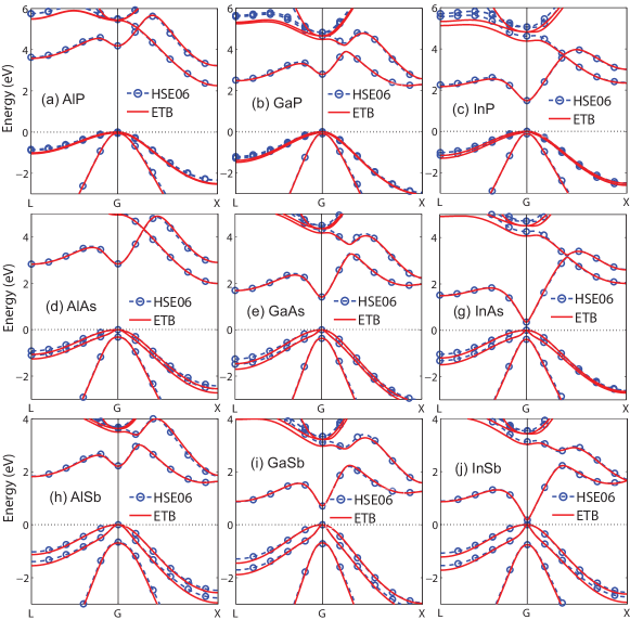
Fig. 3 and 4 show band structures of unstrained bulk band structure for group IV and III-V materials. The presented materials include Si, Ga, XP, XAs and XSb with X = Al,Ga,In. It can be seen that the ETB results of unstrained bulk group IV and III-V materials match corresponding HSE06 results well. Tables 6,7,8 and 9 compare the effective masses and critical band edges between ETB and HSE06 calculations. Most of the effective masses of important valence and conduction valleys are within 10% error. Effective masses of higher conduction valleys like or L valleys tend to have larger error. Discrepancies of critical band edges at high symmetric points between ETB and HSE06 are within 10meV.
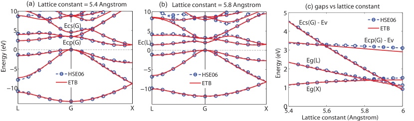
Fig.5 shows Si band structures under hydrostatic strain. The hydrostatic strain does not change crystal symmetry, thus the degeneracy at high symmetry points conserve under hydro static strain. However, it can be observed by comparing Fig.5 (a) and (b) that the hydrostatic strains change the band edges significantly. With a lattice constant of , the lowest conduction bands of Si are valleys, the and s-type valley (Ecs(G)) are of more than 1eV above the valleys. However, with a larger lattice constant of , the and gap descend dramatically , while the gap even increase slightly. The change of band gaps are shown clearly by Fig.5 (c), it can be seen that at around , the and s-type valley become lower than the valleys. As the lattice constant increase more, Si becomes a direct gap material (lowest conduction band is valley). In fact, if the lattice constant is sufficiently large, Si becomes a metal as the s-type valley conduction band become even lower than the valence bands. The trend shown by Fig.5 is valid for other group IV and III-V materials which have diamond or zincblende structures.
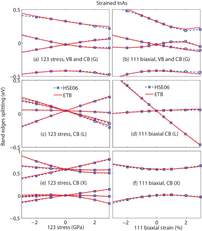
Fig. 7 shows the band edge splitting at , and points of InAs under different strains (strain produced by uniaxial stress along [123] direction and biaxial strain along [111]). The strain presented were not considered in the fitting process and produces complicated bandedge splitting especially for X and L valleys. It can be seen that the ETB band edge splittings are in good agreement with the corresponding HSE06 results. To quantitatively estimate the discrepancies between ETB and HSE06 calculations for strained materials, the deformation potentials are extracted from both ETB and HSE06 results. The deformation potentials of group IV and III-V materials are compared in tables 10 and 12. It can be seen that the important deformation potentials by ETB agree well with the HSE06 results. The discrepancies are within 2%. The deformation potentials and describe the band edge splitting of valence bands under diagonal and off-diagonal strain components respectively. and describe the conduction band edge splitting at X points due to diagonal and off-diagonal strain components respectively. The definition of those deformation potentials are specified in Appendix C.
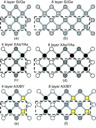
III.4 Tight binding analysis of superlattices
To investigate the transferability of our ETB parameters,band structures of group IV and group III-V superlattices are calculated by both ETB and HSE06 models. The atom structures of the superlattices considered in this work are shown in Fig.8. The superlattices considered in this work grow along 001 direction. Those superlattices contain only a few layers of atoms (with thickness from about 0.5 nm to 1.5 nm). To model those superlattices by ETB method, in principle, self-consistent ETB calculations with Possion equation should be applied if there is charge redistribution in the hetero-structures. However the presented superlattices turn out to be either type I or type II heterojunctions as the ab-initio band structures shows band gap of at least 0.5eV for all the presented superlattices. The charge redistribution in type I or II heterostructures under zero temperature is negligible because the valence bands of both materials are perfectly occupied. The negligible build-in field can also be realized by looking at the envelope of ab-initio local potentialsVan de Walle (1989); Van de Walle and Martin (1986). Thus, the presented ETB calculations for superlattices all assumes zero build-in potentials. The parameter are all set to zero in order to compare with ab-initio results.

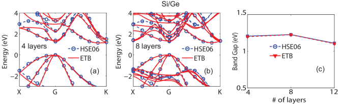
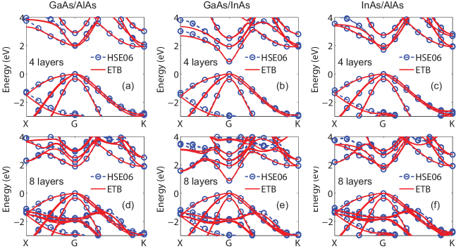
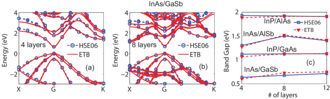
Fig. 9 and Fig. 10 show the comparison of band structures of Si/Ge and Arsenides superlattices by ETB and Hybrid functional calculations respectively. In these figures, band structures of Si/Ge, GaAs/AlAs, GaAs/InAs and InAs/AlAs superlattices are presented. In both ETB and hybrid functional calculations, zero temperature is assumed. For each type of superlattices, band structure of two different unit cells are shown. It can be seen that the ETB band structures are in good agreement for energy from -2eV to 1eV above lowest conduction bands. ETB band structures are obtained with the parameters given by previous sections without introducing extra fitting parameters. From Fig. 9 and Fig. 10, it can be seen that ETB calculations without solving Poisson equation (zero build-in potential is added ) match the HSE06 results well. More complicated cases include InAs/GaSb superlattices which contain no common cations or anions at material interface. The InAs/GaSb superlattices with 4 atomic layers can also be interpreted as InSb/GaAs superlattice. From Fig. 12 (a) and (b), it can be seen that ETB calculations match the HSE06 results well even for interfaces with no common cations or anions.
In 001 superlattices, the primitive unit cells are defined by vectors and , where can be any integer number. According to the theory of Brillouin zone foldingBoykin and Klimeck (2005); Boykin et al. (2007a, b); Popescu and Zunger (2012), the points along [001] direction in a fcc Brillouin zone is folded to the point in the Brillouin zone of superlattices. As a result, the lowest few conduction states at of 001 superlattices can have the feature of and conduction valleys in pure materials. The and conduction valleys can be easily distinguished by the corresponding ETB wave functions. Considering the valleys in a fcc Brillouin zone, the lowest conduction states at point are dominated by s and s* orbitals; while the conduction states at points have significant contribution from both s and p orbitals. This can also be realized by the effective masses of the valleys. The folded X conduction valleys have anisotropic effective masses as it is shown in Fig.10 (a) and (d); while the valley have isotropic effective masses as in Fig.10 (b) and (e). It can be seen from Fig.10 that the lowest conduction state in AlAs/GaAs superlattices have the feature of X conduction valley; while in InAs/GaAs and InAs/AlAs superlattices, the lowest conduction state has the feature of valley.
Fig. 9 (c), Fig.11 and Fig.12 (c) compare the ETB band gap of for different superlattices with corresponding HSE06 results. Fig. 9 (c) shows the band gaps in Si/Ge superlattices. The compared superlattices in Fig.11 include superlattices with common anions (XP/YP, XAs/YAs and XSb/YSb) and superlattices with common cations (AlX/AlY, GaX/GaY and InX/InY). Fig.12 (c) shows the band gaps of selected AX/BY type superlattices, including InAs/GaSb, InAs/AlSb, InP/GaAs and InP/AlAs. For the superlattices shown in the figure, averaged lattice constant is used to create the unit cell of the superlattices since lattice mismatch always exists in superlattices. It can be seen that ETB methods in this work delivered accurate band gaps for ultra small superlattices. For ultra small superlattices, the band gaps are not always monotonic functions of thickness. This non-monotonic dependency of band gaps can be seen in many of the presented superlattices which have common cations (Fig.11 (d), (e) and (f)). The ETB band gap of superlattices agree well with corresponding HSE06. For superlattices which contain common cations or anions (shown in Fig.11), the largest discrepancy of about 0.03eV appears in GaP/GaSb superlattices. While the discrepancy of superlattices which contain no common cation or anions, the largest discrepancy reaches a slightly higher of about 0.05eV. These comparisons suggest that the ETB model and parameters by this work has good transferability.
IV Conclusion
Environment dependent ETB model with nearest neighbor interactions is developed. ETB parameters for group IV and III-V semiconductors are parameterized with respect to HSE06 calculations. Good agreements are achieve for unstrained and arbitrarily strained materials. The ETB parameters show good transferability when applied to ultra-small superlattices. The ETB band structures of superlattices match the corresponding HSE06 result well. Tight binding band gaps of varieties of superlattices show less than 0.1 eV discrepancies compared with HSE06 calculations. This work demonstrated that an ETB model with good transferability can be achieved with nearest neighbor interactions for group IV and III-V materials.
Acknowledgements.
The use of nanoHUB.org computational resources operated by the Network for Computational Nanotechnology funded by the US National Science Foundation under Grant Nos. EEC-0228390, EEC-1227110, EEC-0634750, OCI-0438246, OCI-0832623 and OCI-0721680 is gratefully acknowledged. Samik Mukherjee and Evan Wilson from Network for Computational Nanotechnology, Purdue University are acknowledged for helpful discussion and suggestions.Appendix A Expression of
For a unit vector , the explicit form of are given as follows. For p and d orbitals, the order of orbitals are arranged according to quantum number , with and . Here the are written as matrices with and as row and column indices respectively.
The matrix is given by
| (25) |
The matrix is given by
| (26) |
The matrix is given by
| (27) |
The matrix is given by
| (28) |
Appendix B Dipole potentials
The interatomic coupling due to multipole was given by equation (II.4). For dipole moment, the term are given by equations (25) and (26). The explicit form of are given in this appendix. For example,the couplings is given by
The ’s are two center integrals given by equation (18). Using the explicit expression of and Slater Koster formula of , the terms in equation (B) are written as
| (30) | |||||
| (31) | |||||
The and , satisfying and with and given by equations (20) and (22). It can be seen that the terms with or has resemblance with Slater Koster formula of . To make the expression simpler, in this work, only the terms with and are preserved. Let
| (32) | |||||
| (33) |
The can be approximated by
| (34) |
here the and are defined by
| (35) | |||||
| (36) |
The , , and are given by equations (20) and (22). Similar process can be applied to other ’s. The generalized approximation was summarized by equation (19).
Appendix C deformation potential
-
•
deformation potentials of top valence bands is defined by a 4 band Luttinger k.p Hamiltonian at point.
(37) with
(38) (39) (40) (41) This 4 band Hamiltonian describe the strain behavior top valence bands of zincblende and diamond structures. describe the the Hole splitting under 001 strains( ). describes the Hole splitting under shear components (, , ).
-
•
the deformation potential of CB(X valleys)Yu and Manuel (1964),
(42) where is the strain tensor, is a unit vector along the direction of one of the conduction band minima.
and the deformation potential of conduction X valleys due to is described by 2 band Hamiltonian
(43)
This Hamiltonian describes the upper and lower conduction bands at point of zincblende and diamond structures. The energy difference between the upper and lower conduction bands has the relation
References
- Choi et al. (2007) W. Y. Choi, B.-G. Park, J. D. Lee, and T.-J. K. Liu, Electron Device Letters, IEEE 28, 743 (2007), ISSN 0741-3106.
- Appenzeller et al. (2004) J. Appenzeller, Y.-M. Lin, J. Knoch, and P. Avouris, Phys. Rev. Lett. 93, 196805 (2004), URL http://link.aps.org/doi/10.1103/PhysRevLett.93.196805.
- Zhang et al. (2008) Q. Zhang, T. Fang, H. Xing, A. Seabaugh, and D. Jena, Electron Device Letters, IEEE 29, 1344 (2008), ISSN 0741-3106.
- Gnani et al. (2011) E. Gnani, P. Maiorano, S. Reggiani, A. Gnudi, and G. Baccarani, in Electron Devices Meeting (IEDM), 2011 IEEE International (2011), pp. 5.1.1–5.1.4, ISSN 0163-1918.
- Long et al. (2014) P. Long, M. Povolotskyi, B. Novakovic, T. Kubis, G. Klimeck, and M. Rodwell, Electron Device Letters, IEEE 35, 1212 (2014), ISSN 0741-3106.
- Heyd et al. (2006) J. Heyd, G. Scuseria, and M. Ernzerhof, J. Chem. Phys. 124, 219906 (2006).
- Krukau et al. (2006) A. Krukau, O. Vydrov, A. Izmaylov, and G. Scuseria, J. Chem. Phys. 124, 224106 (2006).
- Hedin (1965) L. Hedin, Phys. Rev. 139, A796 (1965).
- Hybertsen and Louie (1986) M. S. Hybertsen and S. G. Louie, Phys. Rev. B 34, 5390 (1986).
- Ismail-Beigi and Louie (2003) S. Ismail-Beigi and S. G. Louie, Phys. Rev. Lett. 90, 076401 (2003).
- Bahder (1990) T. B. Bahder, Phys. Rev. B 41, 11992 (1990), URL http://link.aps.org/doi/10.1103/PhysRevB.41.11992.
- Tan et al. (2008) Y. Tan, X. Li, L. Tian, and Z. Yu, Electron Devices, IEEE Transactions on 55, 1386 (2008), ISSN 0018-9383.
- Huang et al. (2013) J. Z. Huang, W. C. Chew, J. Peng, C. Y. Yam, L. J. Jiang, and G. H. Chen, IEEE Transactions on Electron Devices 60, 2111 (2013), ISSN 0018-9383.
- Fischetti and Laux (1996) M. V. Fischetti and S. E. Laux, Journal of Applied Physics 80 (1996).
- Jancu et al. (1998) J.-M. Jancu, R. Scholz, F. Beltram, and F. Bassani, Phys. Rev. B 57, 6493 (1998).
- Boykin et al. (2002) T. B. Boykin, G. Klimeck, R. C. Bowen, and F. Oyafuso, Phys. Rev. B 66, 125207 (2002).
- Fonseca et al. (2013) J. Fonseca, T. Kubis, M. Povolotskyi, B. Novakovic, A. Ajoy, G. Hedge, H. Ilatikhameneh, Z. Jiang, P. Sengupta, Y. Tan, et al., Journal of Computational Electronics 12, 592 (2013).
- Klimeck et al. (2002) G. Klimeck, F. Oyafuso, T. B. Boykin, C. R. Bowen, and P. V. Allmen, Computer Modeling in Engineering and Science (CMES) 3, 601 (2002).
- Lake et al. (1993) R. Lake, G. Klimeck, and S. Datta, Phys. Rev. B 47, 6427 (1993).
- Harrison (1999) W. Harrison, Elementary Electronic Structure (World Scientific, 1999), revised edition ed.
- Tserbak et al. (1993) C. Tserbak, H. M. Polatoglou, and G. Theodorou, Phys. Rev. B 47, 7104 (1993), URL http://link.aps.org/doi/10.1103/PhysRevB.47.7104.
- Podolskiy and Vogl (2004) A. V. Podolskiy and P. Vogl, Phys. Rev. B 69, 233101 (2004).
- Niquet et al. (2009) Y. M. Niquet, D. Rideau, C. Tavernier, H. Jaouen, and X. Blase, Phys. Rev. B 79, 245201 (2009).
- Boykin et al. (2010) T. B. Boykin, M. Luisier, M. Salmani-Jelodar, and G. Klimeck, Phys. Rev. B 81, 125202 (2010), URL http://link.aps.org/doi/10.1103/PhysRevB.81.125202.
- Tan et al. (2015) Y. P. Tan, M. Povolotskyi, T. Kubis, T. B. Boykin, and G. Klimeck, Phys. Rev. B 92, 085301 (2015), URL http://link.aps.org/doi/10.1103/PhysRevB.92.085301.
- Tan et al. (2013) Y. Tan, M. Povolotskyi, T. Kubis, Y. He, Z. Jiang, G. Klimeck, and T. Boykin, Journal of Computational Electronics 12, 56 (2013), ISSN 1569-8025.
- Edmonds (1976) A. R. Edmonds, Angular Momentum in Quantum Mechanics (Princeton University Press, Philadelphia, 1976).
- Gaunt (1929) J. A. Gaunt, Phil. Trans. Roy. Soc. A228, 151 (1929).
- Slater and Koster (1954) J. C. Slater and G. F. Koster, Phys. Rev. 94, 1498 (1954).
- Madelung (1991) O. Madelung, Semiconductors: Group IV Elements and III-V Compounds (Springer, 1991).
- Vurgaftman et al. (2001) I. Vurgaftman, J. R. Meyer, and L. R. Ram-Mohan, Journal of Applied Physics 89 (2001).
- Kresse and Furthmuller (1996) G. Kresse and J. Furthmuller, Computational Materials Science 6, 15 (1996), ISSN 0927-0256.
- Kim et al. (2009) Y. Kim, K. Hummer, and G. Kresse, Phys. Rev. B 035203 80 (2009).
- Perdew et al. (1996) J. P. Perdew, K. Burke, and M. Ernzerhof, Phys. Rev. Lett. 77, 3865 (1996).
- Kresse and Joubert (1999) G. Kresse and J. Joubert, Rhys. Rev. B 59, 1758 (1999).
- Van de Walle (1989) C. G. Van de Walle, Phys. Rev. B 39, 1871 (1989), URL http://link.aps.org/doi/10.1103/PhysRevB.39.1871.
- Van de Walle and Martin (1986) C. G. Van de Walle and R. M. Martin, Phys. Rev. B 34, 5621 (1986), URL http://link.aps.org/doi/10.1103/PhysRevB.34.5621.
- Boykin et al. (2004) T. B. Boykin, G. Klimeck, and F. Oyafuso, Phys. Rev. B 69, 115201 (2004).
- Boykin and Klimeck (2005) T. B. Boykin and G. Klimeck, Phys. Rev. B 71, 115215 (2005), URL http://link.aps.org/doi/10.1103/PhysRevB.71.115215.
- Boykin et al. (2007a) T. B. Boykin, N. Kharche, G. Klimeck, and M. Korkusinski, Journal of Physics: Condensed Matter 19, 036203 (2007a), URL http://stacks.iop.org/0953-8984/19/i=3/a=036203.
- Boykin et al. (2007b) T. B. Boykin, N. Kharche, and G. Klimeck, Phys. Rev. B 76, 035310 (2007b), URL http://link.aps.org/doi/10.1103/PhysRevB.76.035310.
- Popescu and Zunger (2012) V. Popescu and A. Zunger, Phys. Rev. B 85, 085201 (2012), URL http://link.aps.org/doi/10.1103/PhysRevB.85.085201.
- Yu and Manuel (1964) P. Yu and C. Manuel, Fundamentals of Semiconductors (Springer, 1964), fourth edition ed.