Resonance effects in the Raman scattering of mono- and few layers MoSe2
Abstract
Using resonant Raman scattering spectroscopy with 25 different laser lines, we describe the Raman scattering spectra of mono- and multi-layers 2H-molybdenum diselenide (MoSe2) as well as the different resonances affecting the most pronounced features. For high-energy phonons, both A- and E- symmetry type phonons present resonances with A and B excitons of MoSe2 together with a marked increase of intensity when exciting at higher energy, close to the C exciton energy. We observe symmetry dependent exciton-phonon coupling affecting mainly the low-energy rigid layer phonon modes. The shear mode for multilayer displays a pronounced resonance with the C exciton while the breathing mode has an intensity that grows with the excitation laser energy, indicating a resonance with electronic excitations at energies higher than that of the C exciton.
pacs:
73.22.Lp, 63.20.Kd, 78.30.Na, 78.67.-nLayered transition-metal dichalcogenides (MX2) are today the subject of intense studies because of the possibility to isolate a single monolayer, a two dimensional crystal, out of the bulk material Mak et al. (2010); Wang et al. (2012). This family of materials includes semiconducting compounds (MX2 with M=Mo or W and X= S, Se, or Te). They offer an interesting platform to explore purely two-dimensional excitons, phonons, and to study the interplay between the spin and valley physics Xiao et al. (2012); Xu et al. (2014). Monolayers of these materials can be transferred on adapted substrates for optical or transport investigations. In contrast to gapless graphene, their band gap of eV allows for the construction of transistors Radisavljevic et al. (2011) and of photodetectors Yin et al. (2012). Even though the room temperature electronic mobilities they exhibit reach only the level of few hundreds , orders of magnitude below what is achieved in conventional III-V or II-VI semiconductors quantum wells, their flexibility and transparency are extremely appealing for future electronic and optoelectronic applications. For instance, they are used as building blocks of van der Waals heterostructures Georgiou et al. (2013); Geim and Grigorieva (2013); Withers et al. (2015), which cannot be controlled without a deep knowledge of the phonon modes and of the electron-phonon interaction in the individual layers. It is also worth to point out that the photoluminescence (PL) of MX2 monolayers arises from tightly bound excitons He et al. (2014); Chernikov et al. (2014), with binding energies close to meV, and hence comparable to those usually observed in molecules or in carbon nanotubes Scholes and Rumbles (2006); Ugeda et al. (2014).
Raman scattering plays an important role in the rapid development of the field of research of 2D crystals as it provides, for most layered materials, a fast and non-invasive tool to determine the number of layers of a given specimen Lee et al. (2010): When the thickness of a MX2 flake is reduced, the energy of some optical phonons changes in a way that can be traced using standard techniques. Resonant Raman scattering is powerful technique to explore electronic properties of materials. The resonant enhancement of Raman scattering signals when the laser energy is tuned to particular values corresponding to electronic excitations of the investigated system, is a well established tool to perform, for instance, the spectroscopy of weakly radiative excitations. This technique has been applied to MoS2 thin layers, probably the most explored layered MX2 so far, and to WSe2 Golasa et al. (2014a); del Corro et al. (2014); Carvalho et al. (2015); Scheuschner et al. (2015); Lee et al. (2015a).
The Raman spectrum of bulk 2H-MoSe2 has been measured in 1980 Sekine et al. (1980), allowing for the identification of the main Raman-active phonon modes of this compound. Since that time, only few studies reported the Raman spectrum of thin layers of this material Tongay et al. (2012); Tonndorf et al. (2013); Kumar et al. (2014). Although they provided the description of the main phonon modes, a complete characterization of the Raman scattering spectrum of thin layers of MoSe2 is still lacking. The phonon band structure of monolayer MoSe2 has recently been calculated by ab-initio techniques Horzum et al. (2013), and this compound appears to be distinct from other member of the MX2 family. All these materials present 6 optical and 3 acoustical phonon branches, but, in contrast to the case of MoS2, WS2 or WSe2 Molina-Sánchez and Wirtz (2011), according to these calculations, in MoSe2 the A’1 mode is located between the E’ and E” modes and is not the highest Raman-active mode at the point of the phonon band structure. The phonon mode of E symmetry around cm-1, measured at nm, has a much weaker intensity than the A1 mode Kumar et al. (2014) close to cm-1. The E’ mode is split over the whole phonon Brillouin zone, with a splitting of cm-1 at the point. These two E’ phonons are of longitudinal (LO) and of transverse character (TO), and their splitting comes from the polar character of MoSe2.
Resonant studies with a large number of laser lines spanning from the near infrared to the ultraviolet are seldom done, and this is particularly difficult and absent in the literature when low energy excitations are involved. It is such a systematic and comprehensive study that is being reported here, for a model MX2 material (MoSe2) from monolayer to multi-layer structures. We present a resonant Raman scattering investigation of mono- and multilayer 2H-MoSe2 using different laser excitation lines from nm ( eV) to nm ( eV), which span the energies of the three different excitons A, B and C, located close to , and eV, respectively Li et al. (2014), and including both high and low energy vibrations. In the first part, we focus on monolayer MoSe2 (1L-MoSe2), discussing in particular the identification of the main Raman scattering features and their excitation profiles. We then address the case of multilayer MoSe2 (NL-MoSe2 where N is the number of layers) and describe the phonon modes which are only Raman-active in multi-layers. These modes have been observed in MoTe2 Yamamoto et al. (2014); Ruppert et al. (2014); Froehlicher et al. , MoS2 Scheuschner et al. (2015), WSe2 Luo et al. (2013); Terrones et al. (2014), and we propose here their proper identification in MoSe2, based on polarization resolved measurement and on resonant Raman scattering experiments. We present the excitation profiles of the main Raman features, including the low energy shear and breathing modes in the case of 2L-MoSe2, and provide evidence, for some of these modes, of an increase of the scattering efficiency at energies beyond that of the C exciton.
Raman scattering experiments were performed at room temperature in the backscattering geometry with a triple-grating spectrometer equipped with a nitrogen cooled charge coupled device (CCD) camera. Laser excitation was provided by a mixed Ar/Kr laser (from 458 to 676 nm) and by a Ti:Sapph laser (from 680 nm to 825 nm). Laser lines were filtered with a grating used in the Littrow configuration. A 50x objective was used to focus the excitation laser down to a spot of m, with optical power of mW. Thin flakes of MoSe2 were first exfoliated from bulk MoSe2 purchased from HQ graphene and then deposited on a Si/SiO2 substrate with a SiO2 thickness of nm. Flakes composed of 1 to 8 layers were identified by their different optical contrast contrast (calibrated with AFM measurements on other flakes) and then by low energy Raman scattering and photoluminescence experiments. Raman scattering spectra were normalized by the integrated intensity of the silicon peak and by its resonant excitation wavelength dependence Renucci et al. (1975), and by the effect of interferences in the SiO2 layer Li et al. (2012) (see appendix). The luminescence background in the case of 1L and 2L has been removed from the presented spectra. In the following, the intensity of each mode is normalized to its maximum value observed in the investigated excitation energy range. We are interested in the independent evolution of the different modes and not by their relative intensities. The vibration patterns of MX2 has been described in many recent reports Zhang et al. (2013); Zhao et al. (2013). Bulk 2H-MX2 belongs to the point group, while their odd and even few layers counterparts represent the and point groups, respectively. This implies a change of the symmetry of the phonon modes depending on the number of layers. In what follows we will use the previously introduced notation Scheuschner et al. (2015), indicating the symmetry of the different phonon modes by a double notation corresponding to the odd and even number of layers.
In Fig. 1a-c we present three Raman scattering spectra of monolayer MoSe2 measured at nm (panel a), at nm (panel b) and at nm (panel c). The scale of these spectra is set in order to compare the position of the different features and normalized spectra are presented in Fig. 1d. With a nm excitation, the most prominent feature is the A’1 mode observed at cm-1 in 1L-MoSe2. Its intensity is 10 times bigger than the intensity of all other Raman scattering features. The E’ mode, predicted to be Raman-active in Ref. [Horzum et al., 2013] is also observed at cm-1. These are the two main features of the Raman scattering spectrum of 1L-MoSe2 Tongay et al. (2012); Tonndorf et al. (2013); Kumar et al. (2014); Late et al. (2014).
A more detailed investigation shows that, similar to other MX2 Berkdemir et al. (2013); Chakraborty et al. (2013); Golasa et al. (2014a, b); Lee et al. (2015b) compounds, acoustical phonons also contribute to the Raman scattering spectrum of 1L-MoSe2 and that depending on the excitation wavelength, such contribution can be strongly enhanced (see e.g. the spectra measured using nm and nm laser excitations). Because the dispersion of acoustical phonons close to the M and K points is rather flat Horzum et al. (2013), the associated density of states is peaked close to this energy and defect mediated phonon scattering is favored. We observe the longitudinal acoustical phonon from the M-K points (LA(M)) at cm-1 and its first overtones (2LA(M), 3LA(M) and 4LA(M)). Next we see a combination of optical and acoustical phonons from the M point, namely A’1(M)LA(M) at and cm-1, respectively, A’1(M)+2LA(M) at cm-1, and E’(M)+LA(M) as well as E’(M)+2LA(M) at and cm-1, respectively. One can also notice in our experimental data the TA(M)+ XLA(M) with X to at , and cm-1. These acoustical phonons features are observed on freshly exfoliated MoSe2 flakes, and also, with similar intensity, on flakes produced months before.
An additional Raman scattering feature appears at cm-1 on all samples, mono- or multilayers. Polarization-resolved measurements show that this feature is of the A-type symmetry, and it follows the same resonances, discussed in the following, as the main A’1 feature at cm-1. At high excitation energy, we also observe some traces of the modes E” () and A”() at 170 and 354 cm-1, respectively Molina-Sánchez and Wirtz (2011); Horzum et al. (2013), which are normally forbidden for mono-layers in back scattering geometry.
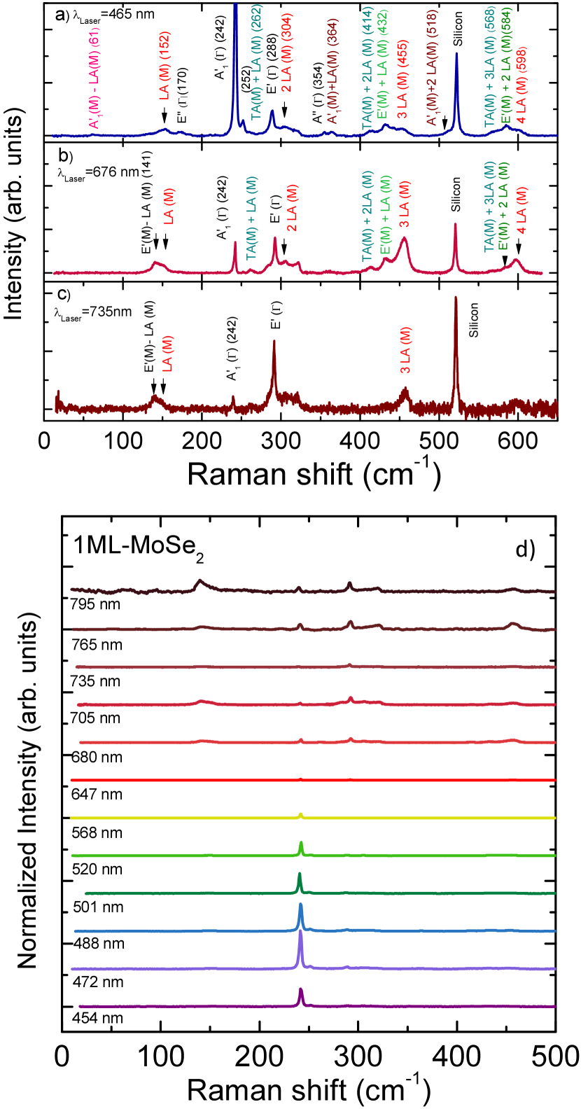
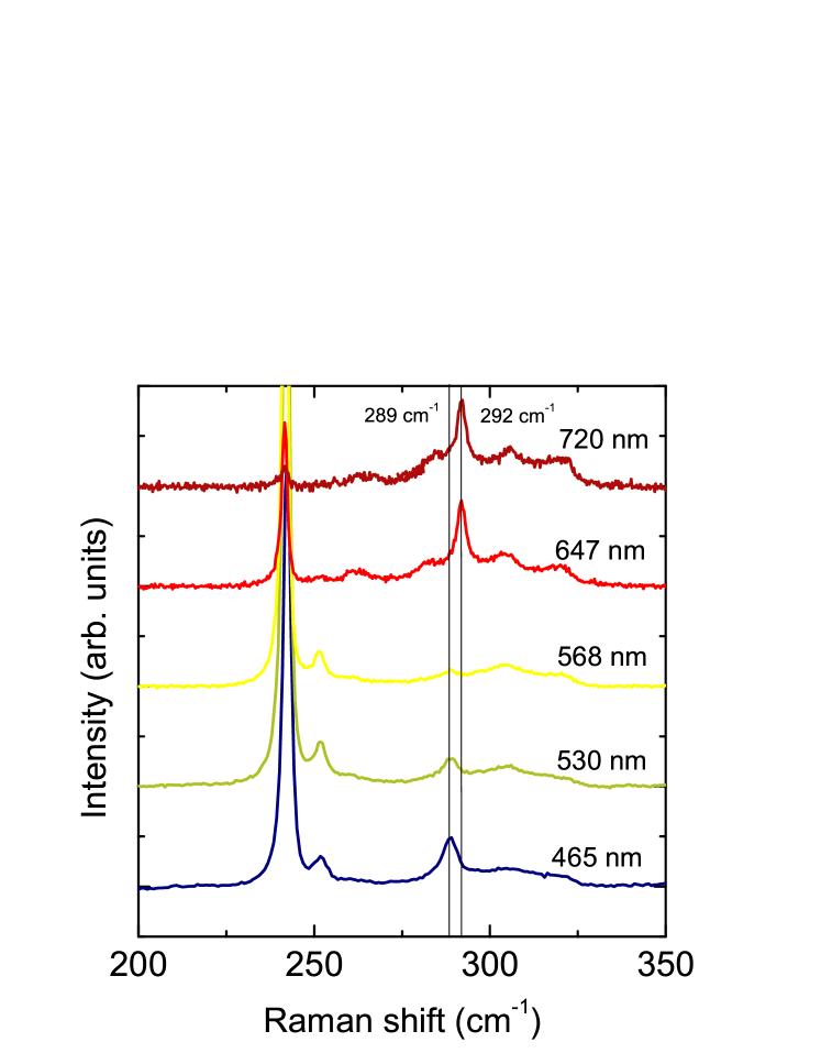
When decreasing the excitation energy using nm or nm excitation (Fig. 1b,c), the Raman scattering spectrum of 1L-MoSe2 changes drastically: the A’1 feature at cm-1, which is prominent at higher excitation energy now has an intensity comparable to that of the acoustical phonon features and of their overtones. The mode TA(M)+LA(M), at cm-1 and the LA(M) overtones also become particularly well visible in this excitation energy regime. The E’() phonon, previously observed at cm-1 now appears at slightly higher energy cm-1, which we tentatively interpret, based on the phonon band structure calculations Horzum et al. (2013), as the selective excitation, for different excitation laser energies, of the lower-energy TO mode or of the upper-energy LO mode Horzum et al. (2013). This crossover is presented in more details in Fig. 2. The lower component of the split E’ mode, prominent for excitation wavelengths below nm, gradually disappears as the excitation wavelength increases. Above nm, the upper component of the split E’ phonon appears at cm-1 with an intensity increasing with the excitation wavelength. As will be confirmed in the following, this behavior suggests a preferential coupling of the LO phonon with the A- and B-type excitons, while the TO phonon can only be observed when exciting at high-energy, in the C exciton range of energy. Such an effect, pronounced in 1L-MoSe2, is also observed in multilayers even though they do not exhibit too strong E’/Eg feature for low excitation energies. We do not have a microscopic explanation for this crossover and for the resonant behavior. Electronic band structure calculations, together with a phonon mode analysis might help in understanding this effect. Such analysis are beyond the scope this experimental paper.
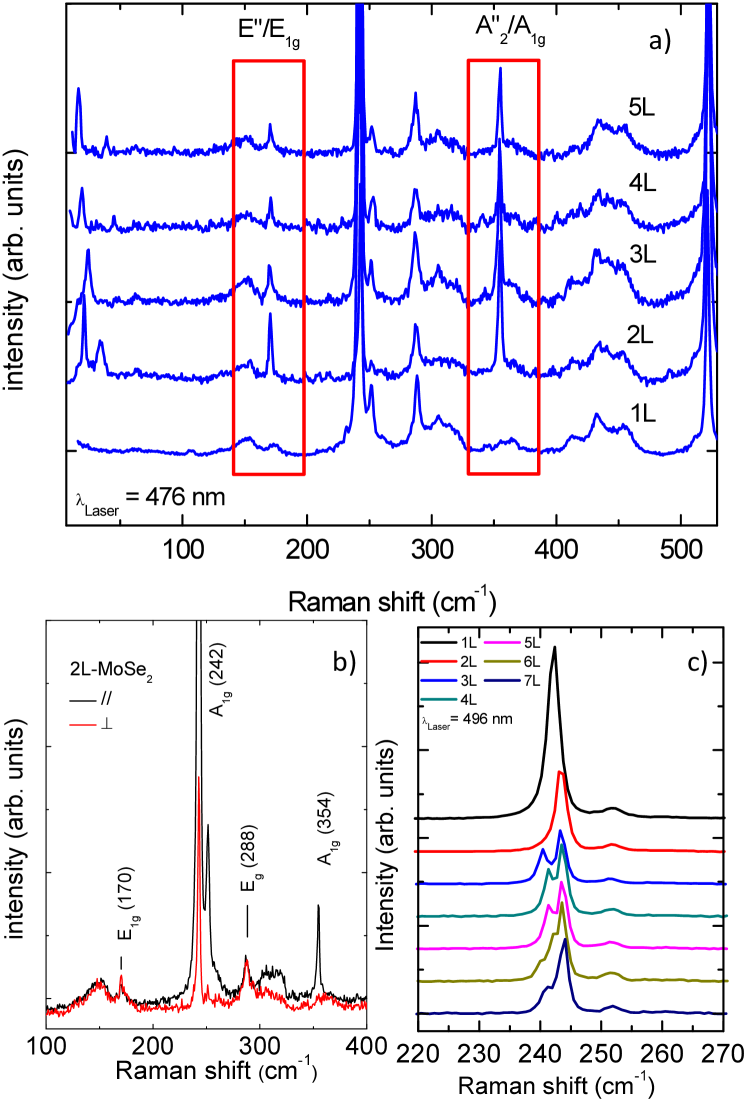
The Raman scattering spectrum of multilayers of MoSe2 shows some additional features. As can be seen in Fig. 3a for 1L- to 5L-MoSe2 two additional peaks, marked by the red boxes, appear at and cm-1 respectively. The energy of these two modes does not depend on the number of layers. In Fig. 3b, we present two Raman scattering spectra measured on a 2L-MoSe2 in the co- and cross-linear polarization configurations. In the cross-linear configuration, the A1g mode at cm-1 is suppressed, together with the mode observed at cm-1, showing that this mode is of A-type symmetry. The feature observed at cm-1 is not affected by the polarization configuration and exhibits hence E-type symmetry. These two features observed at cm-1 and at cm-1 are then attributed to the zone center E”/E1g and A”2/A1g, respectively, and they are not Raman-active in monolayers (even though they show up as weak features when using high excitation energies). Similar Raman scattering results have been recently obtained on MoS2 Scheuschner et al. (2015) and the A”2/A1g was observed in WSe2 Terrones et al. (2014). These latter two modes are not observed in the MoSe2 monolayer, and, as in the case of MoS2, they only appear in multilayers for excitation energies close to the C-exciton energy. The effect have been clearly observed in MoS2 Scheuschner et al. (2015) and these authors explained this observation by the fact that, in contrast to the low-energy A and B excitons whose wave-functions are strongly confined to individual layers, the C exciton’s wave-function is delocalized along the whole structure Qiu et al. (2013); Bradley et al. (2015). As a results, the C exciton can effectively couple to those phonon modes which are characteristic of multilayers and a resonance of the scattered intensity is observed for laser energies close to the C-exciton energy. On the other hand, features of this type do not appear at lower excitation energies, corresponding to the A and B excitons Scheuschner et al. (2015). The observation of these two Raman features can help to quickly discriminate between mono- and multi-layer MoSe2 flakes.
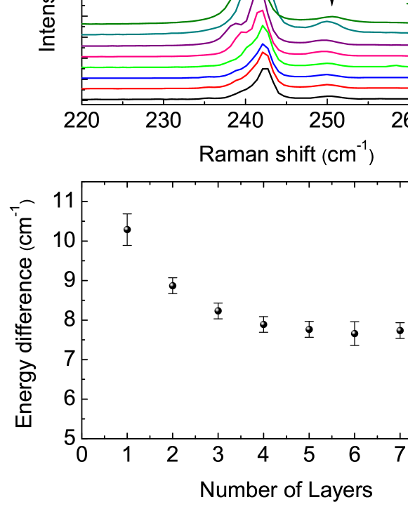
A more detailed knowledge of the number of layers constituting the sample under investigation from Raman scattering experiments can be grasped from the observation of the A’1/A1g feature close to cm-1 (see Fig. 3c). Indeed, as already reported Tonndorf et al. (2013), this peak has an energy that depends on the number of layers, appears in the Raman scattering spectrum as a single component feature for 1L-MoSe2 and 2L-MoSe2, splits into two components for 3L-MoSe2 and 4L-MoSe2 and into three components for 5L-MoSe2 and 6L-MoSe2. The splitting, which comes from interlayer interactions in multilayer materials () Verble and Wieting (1970); Sekine et al. (1980); Froehlicher et al. , can be used to determine the number of layers. Close to cm-1, another Raman scattering feature is observed with an energy that changes with the number of layer. Even though the proper origin of this feature is still unknown, its energy difference with the A’1/A1g feature can provide an additional check for the number of layers of MoSe2 (see appendix). In NL-MoSe2, the contribution of acoustical phonons is also observed in the Raman scattering spectrum in the form of a rich series of overtones, as already discussed in the case of the monolayer.
To complete the description of the differences between mono- and multilayers, we note that another striking difference is seen at low vibrational frequencies, below cm-1. In multilayers, as can be observed in Fig. 3a, some additional features appear in that range with an energy that strongly depends on the number of layers. These modes are the shear and breathing modes of the multilayer structure, i.e. rigid vibrations of the whole layers with respect to each other. The evolution of these modes with increasing number of layers has recently been discussed in the case of MoSe2 Chen et al. (2015). One can notice from the spectra presented in Fig. 3a that, when measured with a nm excitation, the intensity of these modes is comparable with that of the E”/E1g and A”2/A1g modes discussed previously.
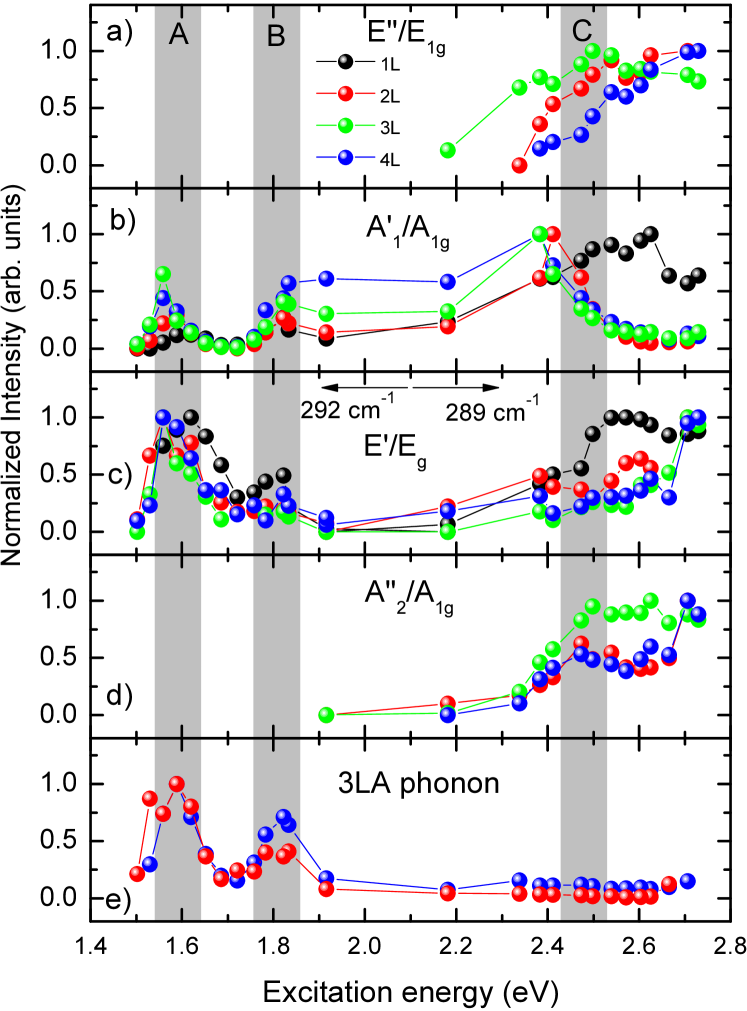
When changing the excitation laser energy, all the Raman scattering features considered so far show particular resonances. These resonances for one- to four- layer flakes, are presented in Fig. 4 for the E”/E1g phonon at 170 cm-1 (panel a), the A’1/A1g phonon close to 242 cm-1 (panel b), the E’/Eg phonon close to cm-1 (panel c), for the A”2/A1g phonon at 354 cm-1 (panel d), and for the 3LA(M) replica (panel d). The E”/E1g and A”2/A1g Raman modes at 170 cm-1 and at 354 cm-1, respectively, typical for multilayers, are only observed for excitation energies above eV. They both exhibit a resonance close to eV. For mono- and multilayers, we observe a resonance of the LO E’/Eg phonon ( cm-1) with the A and B excitons at and eV, respectively, while the TO E’/Eg phonon ( cm-1) has an intensity that increases when exciting at higher energy,close to the C excitons at eV. As a results, in our experiments, these two LO and TO phonons cannot be observed simultaneously. On top of these resonances, the intensity of the TO E’/Eg mode appears to continuously increase when increasing the excitation laser energy. In the case of the monolayer, for which these two features are the most pronounced, the resonance appears at a slightly higher excitation energy, close to eV.
The main A’1/A1g feature close to 242 cm-1 (Fig. 4b) is observed for all samples and shows for the 1L-MoSe2 a resonance at high energy close to eV, which corresponds to the C-exciton energy Li et al. (2014). For higher number of layers, this high energy resonance appears at an energy close to eV. A second resonance is observed at eV and corresponds to the B exciton. Within the resolution of our experiment, the energy of the resonance does not seem to depend on the number of layers. Lowering further the excitation laser energy, another resonance is observed. As for the LO E’/Eg feature, this resonance occurs close to eV and its energy strongly changes with the number of layers. The energies of the A- and of the C- exciton energies appear to depend on the number of layers while the energy of the B excitons does not. Such evolution for the A, B and C excitons as a function of the number of layers has recently been observed in WSe2 and in MoSe2 Arora et al. (2015a, b). These results, concerning the various resonances observed for all the phonon modes of MoSe2, appear as different as compared to the ones reported for MoS2, where the A-type phonon mode shows a resonance with the high-energy exciton only while the E-type modes show a resonance with exclusively the low-energy A and B excitons Carvalho et al. (2015). In MoSe2, the A’1/A1g mode shows clear resonances with all three types of excitons, while the E’/Eg LO phonon displays a resonance with the A and B excitons and the E’/Eg TO phonon only appears at high excitation energy.
Some modes, namely the E’/Eg and the A”2/A1g, have an intensity that, on top of the resonances observed at the exciton energies, increases strongly when increasing the excitation laser energy. This second resonance could be related to the valence band, and especially the band located eV below the highest valence band at the K point Horzum et al. (2013); Ugeda et al. (2014); Wang et al. (2015). In this range of energy, the partial density of states shows a maximum that could explain the resonance behavior observed in Raman scattering. This hypothesis needs to be further clarified on a theoretical point of view and/or with Raman scattering experiments performed in the UV range of energy. Finally, in contrast to the case of optical phonon modes described above, the LA phonon replicas show a pronounced resonance only with the low energy A and B modes, and are only weakly visible when exciting at higher energy. This behavior is shown in Fig. 4e for the 2L and 4L-MoSe2. Similar to the case of MoS2 Golasa et al. (2014a), when using an excitation energy close to that of A or B excitons, these acoustical phonon replica can become the dominant contribution to Raman scattering spectrum of MoSe2 (see spectrum at nm in Fig. 1 and appendix).
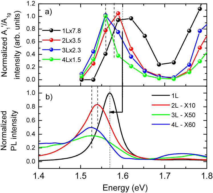
The low-energy resonance of the A’1/A1g mode is presented in more detail in Fig. 5a for excitation energies between 1.4 and 1.8 eV. The photoluminescence (PL) of MoSe2 mono-layers arises from the low-energy A exciton MacNeill et al. (2015). In Fig. 5b, the room-temperature PL spectra recorded on the same samples are plotted for comparison with the data displayed in Fig. 5a.
When increasing the number of layers, we observe at room temperature a marked decrease of the luminescence intensity together with a small shift of the luminescence energy, from eV for 1L-MoSe2, to eV for 2L-MoSe2, and to eV for 3L- and 4L-MoSe2. The origin of these two effects is still debated. They could originate (i) from a direct to indirect band gap transition when going from mono to multilayers, or (ii) reflect the difference in the relative energies of the A exciton and of the single particle indirect bandgap due to the change of dielectric screening and the decrease of the exciton binding energy for multilayers. The observed resonances for the A’1/A1g Raman scattering feature are centered at , , and eV for 1L- to 4L-MoSe2, respectively. We interpret the energy difference between the emission of A excitons and the resonance in the Raman scattering as a signature of an efficient outgoing resonance. In fact, the maximum intensity of the Raman scattering is observed in this material when the incoming photon energy is equal to the sum of the exciton and of the scattered phonon energies.
As already mentioned, layered materials also show low-energy shear phonon modes, of the E-type symmetry, and breathing phonon modes, of the A-type symmetry. Detailed investigation of these modes in few-layer samples has recently become more accessible due to the commercial development of volume Bragg grating filters allowing to easily explore the low-energy range Tan et al. (2012) of the Raman scattering spectrum, down to 5-10 cm-1. The shear and breathing modes are today the subject of intense research in the field of MX2. Their Raman shift as a function of the number of layers and their polarization selection rules have been described in detail for MoS2, WSe2, MoSe2, WS2 and in MoTe2 Zhang et al. (2013); Zhao et al. (2013); Chen et al. (2015); Froehlicher et al. . Because of technical difficulties, such studies are usually performed at a single excitation wavelength, and a complete picture of the excitation profile of such low energy modes in MX2 is still lacking. Resonant Raman spectroscopy of such low-energy modes has been performed in semi-metallic twisted graphene, allowing to trace the evolution of its high-energy bands and to quantify the interlayer interaction as a function of the twist angle Wu et al. (2014).
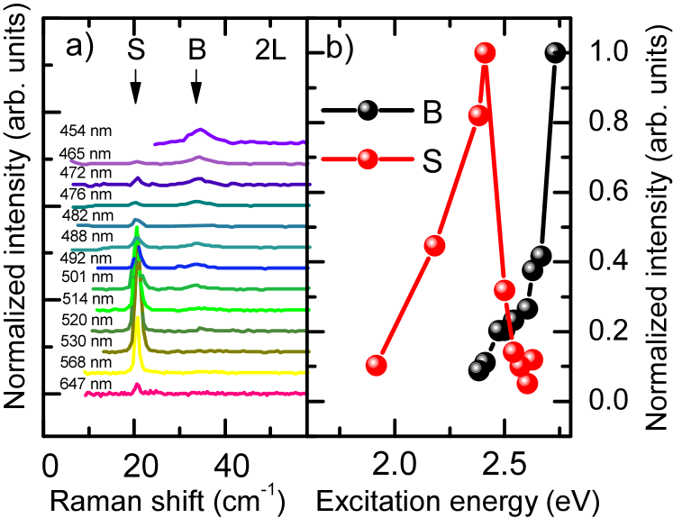
The use of a triple spectrometer and the access to large number of laser lines has allowed us to perform such a detailed resonant study for mono and multilayer MoSe2. In Fig. 6a, we present Raman scattering spectra of the shear (S) and breathing (B) modes of 2L-MoSe2 measured for excitation wavelengths from nm to nm. They are observed at cm-1 and cm-1, respectively Chen et al. (2015) and their energies do not change with the excitation wavelength. Fig. 6b illustrates the evolution of the normalized intensity of these two modes as a function of the excitation laser energy. As can be seen, they show rather distinct resonance behaviors. The E-type symmetry shear mode exhibits a pronounced resonance close to eV, similar to the resonance observed for both high-energy A-type modes, which corresponds to the C exciton energy in 2L-MoSe2. In contrast, the breathing mode, of the A-type symmetry, does not show this resonance but its intensity increases with increasing excitation laser energy. At excitation energies below eV, the intensity of the breathing mode is nearly not observable in 2L-MoSe2, grows rapidly at higher energies, becoming stronger than that of the shear mode and eventually representing the most pronounced low energy feature above eV. For excitation energies lower than eV (647 nm), we could not observe these low-energy modes mainly because of the strong low-energy scattering and/or PL when approaching the energies of the A and B excitons. Similar to the TO E’/Eg at cm-1 and to the A”2/A1g mode at cm-1, the breathing mode’s intensity seems to show a resonance with electronic excitations above the energy of the C exciton. For different MX2 materials, depending on the excitation laser and on the exciton energy structure, very different intensity ratios between the shear and breath modes have been reported recently Zhang et al. (2013); Zhao et al. (2013); Chen et al. (2015); Lee et al. (2015a); Froehlicher et al. . As follows from the study reported here, these differences arise from the peculiar resonance effect affecting differently the two modes.
To conclude, we have presented a comprehensive Raman scattering study of MoSe2 mono- and multi-layers. We have shown in this compound the existence of new Raman modes which are only active in multilayers, and described their resonances when tuning the excitation laser energy across the three different excitons of this material. Resonant Raman spectroscopy appears as a well adapted tool to study a variety of excitons in thin layers of MX2 and their coupling to optical phonons. Our experiments confirm the lowering of the A exciton’s energy when increasing the number of layers and this result is corroborated by the PL measurements. We also show symmetry-dependent exciton-phonon coupling, in particular, we show experimentally that the low-energy shear mode of a bilayer displays a a pronounced resonance with the C exciton while the breathing mode does not. On the other hand, this latter mode, together with the E’/Eg and A”2/A1g mode have an intensity that grows with the excitation laser energy, which is a signature of a still unexplored resonance at higher energy, in the deep UV range.
Acknowledgements.
We acknowledge fruitful discussions with S. Berciaud, M. Molas and with M. Potemski. Part of this work has been supported by the TWINFUSYON project, the graphene flagship project and by the European Research Council (ERC-2012-AdG-320590-MOMB).I Appendix
I.1 Photograph of the different MoSe2 specimens
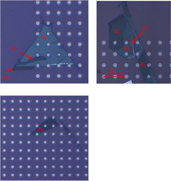
Large flakes of MoSe2 mono- and multi-layers have been produced by mechanical exfoliation of bulk MoSe2. Flakes were then deposited on a Si/SiO2 substrate with nm of SiO2. The substrate had been patterned with circular holes of diameter, but all the results presented in the main text have been obtained on supported regions. The following photograph in Fig. 7 present the different specimens that were used for the reported measurements.
I.2 Raman scattering features at and cm-1
As stated in the main text, MoSe2 mono-layers can be identified by (i) a single component A’1 feature at cm-1 while this feature is observed at cm-1 for 2L and is a multi-component feature for , (ii) the non-observation of the two E”/E1g and A”2/A1g modes at and cm-1, respectively, and (iii) by the observation of an energy separation bigger than cm-1 between the A’1 and the feature close to cm-1 (see Fig. 8. These ar the three Raman scattering signatures of 1L-MoSe2 that emerge from this study.
I.3 Spectra normalization procedure
The normalization of Raman scattering intensities is crucial for the study of resonance effects. All intensities presented in the main text are normalized according to the following procedure: We first make a background correction. This background is most of the case flat but, when the excitation wavelength is set close to the low energy excitons of mono or few layer MoSe2, luminescence signals affect the spectra and are removed but using standard computer tools. Spectra are then normalized by the integrated silicon signal at cm-1. The silicon first order Raman scattering peak shows a resonance when using high excitation energies. This effect was studied in detail in Ref. [Renucci et al., 1975] and has to be taken into account by normalizing the measured signal by the resonance curve of silicon (which also includes the wavelength dependance of the Raman scattering process). Finally, the flake is on top of a SiO2/Si structure which produces optical interferences which have a strong impact on the measured Raman intensities. As it is shown in the literature Yoon et al. (2009); Li et al. (2012); Carvalho et al. (2015), the Raman intensities of the Si and the MoSe2 layers are proportional to an enhancement factor due to the optical interference existent in a multi-layered structure given by:
| (1) |
where and are the electrical field’s amplitude of the total incident and scattered light respectively, and is the thickness of the MoSe2. The enhancement factor for the Si substrate is Li et al. (2012); Carvalho et al. (2015)
| (2) |
where and are the electrical field amplitude of the total incident and scattered light respectively. It is important to take into account the wavelength dependence of the complex refractive index of each materials to describe the propagation of the incident and of the scattered light. In the experiment, the incident wavelength is given by the exciting laser and the Raman process defines the scattered wavelength. To correct the data, we multiply the experimental spectra by the ratio Li et al. (2012); Carvalho et al. (2015) after performing the silicon signal normalization described above.
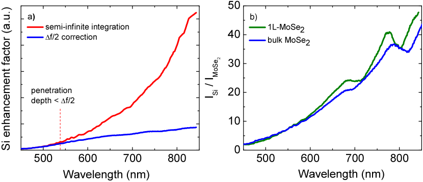
Expression (2) is calculated considering an “unidimensional” problem, where the Si substrate is treated as a half-infinite media. In the IR region, where the Si absorption is small, when using a microscope objective with a large numerical aperture, we should take the divergence effect of the focused gaussian beam into account and calculate the integral in a probed volume defined by the depth of focus. The depth of focus is defined as the distance between the points at each side of the beam-waist where the irradiance of the beam falls to one-half of its value M. Delhaye and Silva (1996). According to Ref. [M. Delhaye and Silva, 1996] it is given by
| (3) |
where is the beam radius at the waist (spot size in the focus) and is the wavelength within the material. Taking that into account, the upper integral limit() must be modified to .
For 1L-MoSe2 sample, Fig. 9a shows the comparison between the semi-infinite integration and the correction for the Si Raman intensity both as a function of wavelength. Here we assumed a Raman shift of 520 cm-1. The complex refractive index for Si and SiO2 as a function of the wavelength were taken from Ref. [Palik, 1998] and Ref. [Malitson, 1965] respectively and the refractive index of 1L-MoSe2 was taken from Ref. [Li et al., 2014]. Fig. 9b shows the ratio of the Si and the MoSe2 enhancement factor as a function of the wavelength for a 1L-MoSe2 and bulk MoSe2 assuming a Raman shift of 290 cm-1. The bulk MoSe2 refractive index was taken from Ref. [Li et al., 2012]. As can be seen, the enhancement factor for 1L-MoSe2 and bulk MoSe2 are similar so that we used the refractive index of the 1L-MoSe2 for the calculations in the multi-layer samples.
References
- Mak et al. (2010) K. F. Mak, C. Lee, J. Hone, J. Shan, and T. F. Heinz, Phys. Rev. Lett. 105, 136805 (2010).
- Wang et al. (2012) Q. Wang, K. Kalantar-Zadeh, A. Kis, J. Coleman, and M. Strano, Nat. Nanotech. 7, 699 (2012).
- Xiao et al. (2012) D. Xiao, G.-B. Liu, W. Feng, X. Xu, and W. Yao, Phys. Rev. Lett. 108, 196802 (2012).
- Xu et al. (2014) X. Xu, W. Yao, D. Xiao, and T. F. Heinz, Nat. Phys. 10, 343 (2014).
- Radisavljevic et al. (2011) B. Radisavljevic, A. Radenovic, J. Brivio, V. Giacometti, and A. Kis, Nat. Nanotech. 6, 147 (2011).
- Yin et al. (2012) Z. Yin, H. Li, H. Li, L. Jiang, Y. Shi, Y. Sun, G. Lu, Q. Zhang, X. Chen, and H. Zhang, ACS Nano 6, 74 (2012).
- Georgiou et al. (2013) T. Georgiou, R. Jalil, B. D. Belle, L. Britnell, R. V. Gorbachev, S. V. Morozov, Y.-J. Kim, A. Gholinia, S. J. Haigh, O. Makarovsky, L. Eaves, L. A. Ponomarenko, A. K. Geim, K. S. Novoselov, and A. Mishchenko, Nat. Nano. 8, 100 (2013).
- Geim and Grigorieva (2013) A. K. Geim and I. V. Grigorieva, Nature 499, 419 (2013).
- Withers et al. (2015) F. Withers, O. Del Pozo-Zamudio, A. Mishchenko, A. P. Rooney, A. Gholinia, K. Watanabe, T. Taniguchi, S. J. Haigh, A. K. Geim, A. I. Tartakovskii, and K. S. Novoselov, Nat. Mat. 14, 301 (2015).
- He et al. (2014) K. He, N. Kumar, L. Zhao, Z. Wang, K. F. Mak, H. Zhao, and J. Shan, Phys. Rev. Lett. 113, 026803 (2014).
- Chernikov et al. (2014) A. Chernikov, T. C. Berkelbach, H. M. Hill, A. Rigosi, Y. Li, O. B. Aslan, D. R. Reichman, M. S. Hybertsen, and T. F. Heinz, Phys. Rev. Lett. 113, 076802 (2014).
- Scholes and Rumbles (2006) G. Scholes and G. Rumbles, Nat. Mat. 5, 683 (2006).
- Ugeda et al. (2014) M. M. Ugeda, A. J. Bradley, S.-F. Shi, F. H. da Jornada, Y. Zhang, D. Y. Qiu, W. Ruan, S.-K. Mo, Z. Hussain, Z.-X. Shen, F. Wang, S. G. Louie, and M. F. Crommie, Nat. Mat. 13, 1091 (2014).
- Lee et al. (2010) C. Lee, H. Yan, L. E. Brus, T. F. Heinz, J. Hone, and S. Ryu, ACS Nano 4, 2695 (2010).
- Golasa et al. (2014a) K. Golasa, M. Grzeszczyk, P. Leszczynski, C. Faugeras, A. A. L. Nicolet, A. Wysmolek, M. Potemski, and A. Babinski, Appl. Phys. Lett. 104 (2014a), 10.1063/1.4867502.
- del Corro et al. (2014) E. del Corro, H. Terrones, A. Elias, C. Fantini, S. Feng, M. A. Nguyen, T. E. Mallouk, M. Terrones, and M. A. Pimenta, ACS Nano 8, 9629 (2014).
- Carvalho et al. (2015) B. R. Carvalho, L. M. Malard, J. M. Alves, C. Fantini, and M. A. Pimenta, Phys. Rev. Lett. 114, 136403 (2015).
- Scheuschner et al. (2015) N. Scheuschner, R. Gillen, M. Staiger, and J. Maultzsch, Phys. Rev. B 91, 235409 (2015).
- Lee et al. (2015a) J.-U. Lee, J. Park, Y.-W. Son, and H. Cheong, Nanoscale 7, 3229 (2015a).
- Sekine et al. (1980) T. Sekine, M. Izumi, T. Nakashizu, K. Uchinokura, and E. Matsuura, Jour. of the Phys. Soc. of Japan 49, 1069 (1980).
- Tongay et al. (2012) S. Tongay, J. Zhou, C. Ataca, K. Lo, T. S. Matthews, J. Li, J. C. Grossman, and J. Wu, Nano Letters 12, 5576 (2012).
- Tonndorf et al. (2013) P. Tonndorf, R. Schmidt, P. Böttger, X. Zhang, J. Börner, A. Liebig, M. Albrecht, C. Kloc, O. Gordan, D. R. T. Zahn, S. M. de Vasconcellos, and R. Bratschitsch, Opt. Express 21, 4908 (2013).
- Kumar et al. (2014) N. Kumar, Q. Cui, F. Ceballos, D. He, Y. Wang, and H. Zhao, Nanoscale 6, 4915 (2014).
- Horzum et al. (2013) S. Horzum, H. Sahin, S. Cahangirov, P. Cudazzo, A. Rubio, T. Serin, and F. M. Peeters, Phys. Rev. B 87, 125415 (2013).
- Molina-Sánchez and Wirtz (2011) A. Molina-Sánchez and L. Wirtz, Phys. Rev. B 84, 155413 (2011).
- Li et al. (2014) Y. Li, A. Chernikov, X. Zhang, A. Rigosi, H. M. Hill, A. M. van der Zande, D. A. Chenet, E.-M. Shih, J. Hone, and T. F. Heinz, Phys. Rev. B 90, 205422 (2014).
- Yamamoto et al. (2014) M. Yamamoto, S. T. Wang, M. Ni, Y.-F. Lin, S.-L. Li, S. Aikawa, W.-B. Jian, K. Ueno, K. Wakabayashi, and K. Tsukagoshi, ACS Nano 8, 3895 (2014).
- Ruppert et al. (2014) C. Ruppert, O. B. Aslan, and T. F. Heinz, Nano Letters 14, 6231 (2014).
- Froehlicher et al. (0) G. Froehlicher, E. Lorchat, F. Fernique, C. Joshi, A. Molina-Sanchez, L. Wirtz, and S. Berciaud, Nano Letters 0, null (0).
- Luo et al. (2013) X. Luo, Y. Zhao, J. Zhang, M. Toh, C. Kloc, Q. Xiong, and S. Y. Quek, Phys. Rev. B 88, 195313 (2013).
- Terrones et al. (2014) H. Terrones, E. Del Corro, S. Feng, J. M. Poumirol, D. Rhodes, D. Smirnov, N. R. Pradhan, Z. Lin, M. A. T. Nguyen, A. L. Elias, T. E. Mallouk, L. Balicas, M. A. Pimenta, and M. Terrones, Scientific Reports 4 (2014), 10.1038/srep04215.
- Renucci et al. (1975) J. B. Renucci, R. N. Tyte, and M. Cardona, Phys. Rev. B 11, 3885 (1975).
- Li et al. (2012) S.-L. Li, H. Miyazaki, H. Song, H. Kuramochi, S. Nakaharai, and K. Tsukagoshi, ACS Nano 6, 7381 (2012).
- Zhang et al. (2013) X. Zhang, W. P. Han, J. B. Wu, S. Milana, Y. Lu, Q. Q. Li, A. C. Ferrari, and P. H. Tan, Phys. Rev. B 87, 115413 (2013).
- Zhao et al. (2013) Y. Zhao, X. Luo, H. Li, J. Zhang, P. T. Araujo, C. K. Gan, J. Wu, H. Zhang, S. Y. Quek, M. S. Dresselhaus, and Q. Xiong, Nano Lett. 13, 1007 (2013).
- Late et al. (2014) D. J. Late, S. N. Shirodkar, U. V. Waghmare, V. P. Dravid, and C. N. R. Rao, ChemPhysChem 15, 1592 (2014).
- Berkdemir et al. (2013) A. Berkdemir, H. R. Gutierrez, A. R. Botello-Mendez, N. Perea-Lopez, A. L. Elias, C.-I. Chia, B. Wang, V. H. Crespi, F. Lopez-Urias, J.-C. Charlier, H. Terrones, and M. Terrones, Scientific Rep. 3 (2013), 10.1038/srep01755.
- Chakraborty et al. (2013) B. Chakraborty, H. Matte, A. Sood, and C. Rao, J. Raman Spectrosc. 44, 92 (2013).
- Golasa et al. (2014b) K. Golasa, M. Grzeszczyk, R. Bozek, P. Leszczynski, A. Wysmolek, M. Potemski, and A. Babinski, Solid State Comm. 197 (2014b), 10.1016/J.ssc.2014.08.009.
- Lee et al. (2015b) J.-U. Lee, K. Kim, and H. Cheong, 2D Materials 2, 044003 (2015b).
- Qiu et al. (2013) D. Y. Qiu, F. H. da Jornada, and S. G. Louie, Phys. Rev. Lett. 111, 216805 (2013).
- Bradley et al. (2015) A. J. Bradley, M. M. Ugeda, F. H. da Jornada, D. Y. Qiu, W. Ruan, Y. Zhang, S. Wickenburg, A. Riss, J. Lu, S.-K. Mo, Z. Hussain, Z.-X. Shen, S. G. Louie, and M. F. Crommie, Nano Lett. 15, 2594 (2015).
- Verble and Wieting (1970) J. L. Verble and T. J. Wieting, Phys. Rev. Lett. 25, 362 (1970).
- Chen et al. (2015) S.-Y. Chen, C. Zheng, M. S. Fuhrer, and J. Yan, Nano Lett. 15, 2526 (2015).
- Arora et al. (2015a) A. Arora, M. Koperski, K. Nogajewski, J. Marcus, C. Faugeras, and M. Potemski, Nanoscale 7, 10421 (2015a).
- Arora et al. (2015b) A. Arora, K. Nogajewski, M. Molas, M. Koperski, and M. Potemski, Nanoscale 7, 20769 (2015b).
- Wang et al. (2015) G. Wang, C. Robert, A. Suslu, B. Chen, S. Yang, S. Alamdari, I. C. Gerber, T. Amand, X. Marie, S. Tongay, and B. Urbaszek, ArXiv e-prints (2015), arXiv:1506.08114 [cond-mat.mtrl-sci] .
- MacNeill et al. (2015) D. MacNeill, C. Heikes, K. F. Mak, Z. Anderson, A. Kormányos, V. Zólyomi, J. Park, and D. C. Ralph, Phys. Rev. Lett. 114, 037401 (2015).
- Tan et al. (2012) P. H. Tan, W. P. Han, W. J. Zhao, Z. H. Wu, K. Chang, H. Wang, Y. F. Wang, N. Bonini, N. Marzari, N. Pugno, G. Savini, A. Lombardo, and A. C. Ferrari, Nat. Mat. 11, 294 (2012).
- Wu et al. (2014) J.-B. Wu, X. Zhang, M. Ijaes, W.-P. Han, X.-F. Qiao, X.-L. Li, D.-S. Jiang, A. C. Ferrari, and P.-H. Tan, Nat. Comm. 5 (2014), 10.1038/ncomms6309.
- Yoon et al. (2009) D. Yoon, H. Moon, Y.-W. Son, J. S. Choi, B. H. Park, Y. H. Cha, Y. D. Kim, and H. Cheong, Phys. Rev. B 80, 125422 (2009).
- M. Delhaye and Silva (1996) J. A. M. B. M. Delhaye, J. Barbillat and E. D. Silva, Raman Microscopy, development and applications (Academic Press, 1996).
- Palik (1998) E. Palik, Handbook of Optical Constants of Solids, Vol. 3 (Academic Press, 1998).
- Malitson (1965) I. H. Malitson, J. Opt. Soc. Am. 55, 1205 (1965).