[table]labelsep=period,labelfont=bf,rm
\captionsetup[figure]labelfont=bf,labelsep=period
UPV/EHU]
Nano-Bio Spectroscopy Group and ETSF Scientific Development Center, Departamento de Física de Materiales, Universidad del País Vasco UPV/EHU and DIPC, E-20018 San Sebastián, Spain
UPV/EHU]
Nano-Bio Spectroscopy Group and ETSF Scientific Development Center, Departamento de Física de Materiales, Universidad del País Vasco UPV/EHU and DIPC, E-20018 San Sebastián, Spain
Theoretical Insight into the Internal Quantum Efficiencies of Polymer/C and Polymer/SWNT Photovoltaic Devices
ABSTRACT:
The internal quantum efficiency (IQE) of an organic photovoltaic device (OPV) is proportional to the number of free charge carriers generated and their conductivity, per absorbed photon. However, both the IQE and the quantities that determine it, for example, electron–hole binding, charge separation, electron–hole recombination, and conductivity, can only be inferred indirectly from experiments. Using density functional theory, we calculate the excited-state formation energy, charge transfer, and zero-bias conductance in the singlet ground state and triplet excited state across polymer/fullerene and polymer/single walled carbon nanotube (SWNT) OPV donor/acceptor bulk heterojunctions. Specifically, we compare polythiophene (PT) and poly(3-methylthiophene-2,5-diyl) (P3MT) as donors and C60 chains with (6,4), (6,5), and (10,5) SWNTs as acceptors. We find the conduc-
![[Uncaptioned image]](/html/1603.04837/assets/x1.png) tivity increases substantially for both the excited triplet relative to the singlet ground state and for PT compared with P3MT due to the increased charge transfer and the resulting improvement in donor/acceptor level alignment. Similarly, the (6,4) SWNT, with a larger SWNT band gap and greater conductivity than fullerenes, provides the highest conductivities of 5 and 9% of the theoretical maximum for electron and hole carriers, respectively. This work has important implications for both the optimization of polymer/SWNT bulk heterojunctions and the design of new OPV bulk heterojunctions in silico.
tivity increases substantially for both the excited triplet relative to the singlet ground state and for PT compared with P3MT due to the increased charge transfer and the resulting improvement in donor/acceptor level alignment. Similarly, the (6,4) SWNT, with a larger SWNT band gap and greater conductivity than fullerenes, provides the highest conductivities of 5 and 9% of the theoretical maximum for electron and hole carriers, respectively. This work has important implications for both the optimization of polymer/SWNT bulk heterojunctions and the design of new OPV bulk heterojunctions in silico.
1. INTRODUCTION
The internal quantum efficiency (IQE) of a type II bulk heterojunction within an organic photovoltaic (OPV) device is simply the ratio of free charge carrier generation to photon absorption at a given photon energy. As such, the IQE depends on the ease of separating electron and holes, and the resulting current through the OPV. The former depends on the electron–hole binding, charge transfer from donor to acceptor, and electron–hole recombination, while the latter depends on the conductance from donor to acceptor across the bulk heterojunction. Note that unlike the photovoltaic efficiency,1 the IQE is independent of the device’s optical absorption spectra, that is, the number of absorbed photons, as it is calculated per absorbed photon.2
To estimate the relative exciton binding between type II bulk heterojunctions, one may compare the first transition for the isolated acceptor, for example, the transition of a nanotube, with the formation energy of the triplet excited state from the singlet ground state, that is, their difference in total energy. A much smaller triplet formation energy for the isolated acceptor, , suggests that electron–hole separation may prove difficult. This is the case for single-walled carbon nanotubes (SWNTs), where the measured singlet exciton binding is eV3, 4, 5, 6, 7. Conversely, if the triplet formation energy in the bulk heterojunction is smaller than that for the isolated acceptor, this is indicative of hole transfer to the donor for type II bulk heterojunctions. In this way, the triplet formation energy can be used to compare the relative ease or difficulty of electron hole separation and the probability of recombination in bulk heterojunctions.
The ease of electron–hole separation in the bulk heterojunction may also be directly probed by considering the difference in charge transfer from donor to acceptor between the triplet excited state and the singlet ground state8, 9. However, although a greater charge transfer in the triplet excited state means the electron and hole are separated onto different molecules in the bulk heterojunction, it does not address whether the separated electron and hole are free charge carriers or remain bound within the junction.
To determine whether separated electrons and holes truly behave as free charge carriers, the degree of scattering, and the resulting current through the OPV, one should compute the conductance across the bulk heterojunction from the donor to the acceptor in the excited state. In particular, one should consider the conductance at the Fermi level of the excited electron/hole to determine the number of free electron/hole carriers.
In this study, we carry out density functional theory (DFT) calculations of the excited-state formation energy, charge transfer, and zero-bias conductance of prototypical donor/acceptor bulk heterojunctions10, 11, 12, 13, 14, 15, 16, 17, 18, 19, 20, 21, 22, 23 in the singlet ground state and triplet excited state. For the donor molecule we employ the prototypical photoactive polymers: polythiophene (PT)24 and poly(3-methylthiophene-2,5-diyl) (P3MT)25. For the acceptor molecule we compare fullerene (C60) chains with semiconducting (6,4), (6,5), and (10,5) SWNTs, whose band gaps range between 1 and 1.4 eV26. These systems exhibit only a minor structural relaxation in the triplet excited state (<25 meV). This justifies our neglect of molecular vibration as a first approximation,27 as done in previous studies of photovoltaic efficiencies.28, 29, 30
We model the excited-state formation energy using the total energy difference between the triplet excited state and the singlet ground state from DFT. To obtain the charge transfer from donor to acceptor in the bulk heterojunction, we perform a simplified Bader analysis31 of the DFT all-electron density. Finally, we calculate the Landauer–Bütticker conductance of electron and hole charge carriers from donor to acceptor across the bulk heterojunction based on the DFT tight-binding Hamiltonians using a multiterminal implementation32 of the nonequilibrium Green’s function (NEGF) method33, 34, 35, 36. In this way, we obtain the conductance from the isolated polymer, through the polymer/SWNT or polymer/C60 heterojunction, and out the SWNT or C60 chain, in the quantum coherent regime. Our use of the NEGF method for calculating the conductance across polymer/SWNT and polymer/C60 heterojunctions is justified by the ballistic transport, long coherence length, and high thermal conductivity of SWNTs37, 38, 32, 39, 40, and the dominance of tunneling in transport processes across C60 chains. This method provides a more sophisticated description of the transport processes, and IQE of the device, than previous studies employing the Newns-Anderson model28, 29, 30.
2. METHODOLOGY
All DFT calculations were performed with locally centered atomic orbitals (LCAOs) and the projector augmented wave (PAW) implementation of the gpaw code 41, 42, 43, within the generalized gradient approximation (PBE)44 for the exchange correlation (xc)-functional. We employed a double-zeta polarized (DZP) LCAO basis set for representing the density, wave functions, and tight-binding Hamiltonian, which yields transmission functions in quantitative agreement ( meV) with plane-wave codes and maximally localized Wannier functions 45. All calculations employed a room temperature Fermi filling ( meV), with total energies extrapolated to K, that is, excluding the electronic entropy contribution to the free energy . In this way we avoided an unrealistic smearing of the excited electron and hole in the triplet excited state calculations. We included two thirds of the number of electrons () many bands within the calculations. This has been shown to be sufficient to converge the first transitions of graphene 46 and SWNT/polymer hybrid systems 47, and the optical spectra of polymers and oligomers48 in the random phase approximation (RPA).
Structural optimization was performed within the atomic simulation environment (ASE) 49, until a maximum force below 0.05 eV/Å was obtained. We employed more than 5 Å of vacuum to the cell boundaries orthogonal to the C60 chain, (6,4), (6,5), (10,5) SWNTs, polythiophene (PT), poly(3-methylthiophene-2,5-diyl) (P3MT), and poly(3-hexylthiophene-2,5-diyl) (P3HT), and obtained the optimized unit cell parameters along their axes 18.811, 40.915, 11.348, 7.867, 7.846, and 7.797 Å, respectively. Here PT, P3MT, and P3HT are modeled using two thiophene, 3-methylthiophene, and 3-hexylthiophene units, respectively, in -trans configuration. To sample the Brillouin zone, we included three points along the axis of PT, P3MT, P3HT, (6,4) SWNT, and (10,5) SWNT and one -point along the axis of the (6,5) SWNT.
The C60/polymer junctions were modeled by aligning 10 thiophene/3-methylthiophene units orthogonal to a chain of three C60 molecules and fully relaxing the resulting structure, shown in Figure 1. The SWNT/polymer junctions were modeled by aligning six thiophene/3-methylthiophene units for the smaller (6,4) and (6,5) SWNTs and eight thiophene/3-methylthiophene units for the (10,5) SWNT orthogonal to the tube, which was repeated once along its axis, and performing single-point calculations for the resulting configurations shown in Figure 1. This repetition of the thiophene/3-methylthiophene units makes a single -point sampling along the polymer axis sufficient for describing the Brillouin zone.
By orienting the polymer and SWNT orthogonal to each other, this configuration describes the limit of a minimal SWNT–polymer overlap. In fact, by orienting diagonally across the SWNT axis a ten thiophene unit oligomer, which should provide a reasonable description of PT48, one obtains a greater charge transfer and stronger hybridization between the polymer and SWNT47.
For the SWNT/polymer junctions, the intermolecular distances were fixed between one carbon atom located at the centered C–C single bond of the polymer and a carbon atom of the tube, which were both aligned in the axis orthogonal to the tube and the polymer axis as shown in Figure 1. The alignment was achieved by shifting the polymer along the tube axis. This chosen intermolecular C–C distance is 3.35 for PT and 3.39 Å for P3MT. We slightly increased the P3MT intermolecular distance to reduce the repulsive forces from the hydrogen atoms of the methyl group. Both minimum distances employed are consistent with the interlayer distance of multiwalled carbon nanotubes (MWNTs) and graphite 50, of Å.
We performed DFT calculations for each system in both the singlet ground state () and triplet excited state (). The triplet excited state calculations were performed by fixing the total magnetic moment of the system, and using separate Fermi levels for the spin majority and minority channels, and , respectively. The Fermi levels associated with electron and hole charge carriers are then simply and , respectively. For the singlet ground state calculations, is approximately the conduction band minimum (CBM) , while is approximately the valence band maximum (VBM) .
The charge densities associated with the excited electron and hole in the triplet state are the negative and positive regions, respectively, of the all-electron charge density difference between that of the triplet excited state () and singlet ground state (), that is, .
To quantify the charge transfer from donor to acceptor, we perform a simplified Bader analysis31 of the all-electron charge density in the singlet ground state and triplet excited state . We begin by integrating the charge density over the plane of the donor and acceptor axes to obtain the linear charge density . We then partition at its minimum in between the polymer and C60 chain or SWNT. The charge transfer from donor to acceptor is then , where is the total number of electrons on the isolated acceptor molecule.
We employ a similar partitioning to assign a Kohn-Sham (KS) orbital to the donor or acceptor molecule of the bulk heterojunction. The fraction of the th KS orbital on the acceptor molecule is then .
The periodic DFT Hamiltonian and overlap matrices in the LCAO basis, and , are employed within the NEGF formalism to calculate the Landauer–Bütticker conductance for a multiterminal configuration34, 36, 32. To do so, one must first remove overlap elements between atomic sites separated by more than half the length of the unit cell along the transmission direction, that is, , to obtain nonperiodic Hamiltonian and overlap matrices and .
The coupling matrix to the semi-infinite leads for the SWNTs is obtained by repeating the periodic DFT Hamiltonian matrix for the isolated SWNT and removing overlap elements between atomic sites separated by more than , yielding the nonperiodic Hamiltonian for semi-infinite lead . This is reasonable for the SWNTs considered herein, for which Å. In this way we avoid performing a DFT calculation with a repeated unit cell to obtain the Hamiltonian of the principle layer, , which only couples to the next principle layer through the coupling matrix . We then align the semi-infinite lead Hamiltonian to the nonperiodic DFT Hamiltonian for the bulk heterojunction using the first onsite energy of the same SWNT carbon atom at the cell boundary. This is unnecessary for PT, P3MT, and C60 because their lead Hamiltonians are extracted directly from the bulk heterojunction Hamiltonian. In these cases two thiophene units, two 3-methylthiophene units, and a C60 molecule comprise a principle layer, with couplings to the next nearest layer numerically zero.
The Hamiltonian matrix for the bulk heterojunction central region, , is then generated by augmenting the nonperiodic DFT Hamiltonian for the junction with the principle layer Hamiltonians and coupling matrices of the semi-infinite SWNT leads. The same procedure is employed to obtain the overlap matrix for the bulk heterojunction central region, .
Following the multiterminal NEGF procedure described in ref 32, the zero-bias conductance at the Fermi level is , where is the quantum of conductance, is the Green’s function of the bulk heterojunction central region, and is the coupling to the semi-infinite input and output leads. The Green’s function of the bulk heterojunction central region is , where is the self-energy of lead , and meV is the electronic broadening applied to both the central region and the semi-infinite leads. The self-energy of lead is , where and are the couplings of lead to the bulk heterojunction central region in the Hamiltonian and overlap matrices, and , respectively. Finally, the coupling to the semi-infinite input/output leads is , where is the self-energy of the input/output lead. The four-terminal conductance across the bulk heterojunction from donor to acceptor is then obtained when the input lead is that of a semi-infinite polymer, and the output lead is that of a semi-infinite C60 chain or SWNT.
The conductance of electron and hole charge carriers is then obtained by simply evaluating the transmission at their associated Fermi levels and , respectively. However, to understand the origin of differences in conductivity between the various donor/acceptor bulk heterojunctions considered herein, we shall find it useful to also consider the transmission within an energy window around the acceptor’s VBM and CBM. In this way, we may differentiate between differences in conductivity owing to an improved level alignment between donor and acceptor, an increased overlap of their levels, or a greater number of available transmission channels.
3. RESULTS AND DISCUSSION
To quantify the differences in electronic properties among the donors (PT, P3MT, and P3HT) and acceptors (C60 chain, (6,4), (6,5), and (10,5) SWNTs), we first consider the energy gaps for the isolated polymers and the band gaps of the isolated fullerene chain and SWNTs. Among the three functionalized thiophene polymers considered, both the calculated Kohn-Sham (KS) energy gaps and those measured via photoluminesence24, 25, 21 differ by less than 50 meV, with the largest difference from polythophene (PT) occurring with the first methyl functionalization group (P3MT). For this reason, along with the accompanying reduction of computational effort, we shall restrict consideration from hereon to PT and P3MT as donors.
The acceptors considered have been intentionally chosen to provide a range of electronic band gaps, as shown in Table 1,
species — — — PT P3MT C60 chain 1.46 1 .9a 1.508 0.842 0.622 (6,4) SWNT 1.08 1 .420b 1.101 0.967 0.843 (6,5) SWNT 0.92 1 .272b 0.853 0.804 0.689 (10,5) SWNT 0.74 0 .992b 0.858 0.712 0.626 aRef 51. bRef 26.
from 1 eV for the (10,5) SWNT to 1.9 eV for the C60 chain. In each case, the calculated KS band gaps differ from the first transition measured in photoluminescence (PL) experiments51, 26 by %. This is consistent with previous results, and may be addressed through many-body corrections to the self energy52, 53, 54. However, for our purposes, it is more relevant to note that the difference is rather systematic among the carbon-based materials considered herein.
A more reliable descriptor for differences in exciton binding between bulk heterojunctions is the triplet excited-state formation energy , provided in Table 1. This is obtained from the total energy difference between a system in the triplet excited state and the singlet ground state, that is, . Because depends only on DFT total energies and not on KS eigenvalues, this quantity is in principle exact up to the approximation for the xc-functional.
Comparing the measured transition energy and the calculated triplet formation energy for the isolated C60 chain and (6,5) SWNT, we find that their difference is eV. This is consistent with the measured singlet exciton binding energy in SWNTs3, 4, 5, 6, 7. Although differences between the excited singlet and triplet states may occur, this demonstrates that the triplet excited state provides a reasonable approximation to the singlet excited state for fullerenes and SWNTs. For the (6,4) SWNT, we obtain a somewhat smaller energy difference (0.3 eV), while for the (10,5) SWNT it is significantly reduced to 0.1 eV. The latter is related to the reduction of the transition energy for the (10,5) SWNT, while the is unchanged relative to the (6,5) SWNT. Altogether, this is indicative of a strong exciton binding in the isolated C60 chain, (6,4) SWNT, and (6,5) SWNT, with a much weaker exciton binding in the (10,5) SWNT. This suggests that charge separation for isolated SWNTs may be easier for those with a smaller band gap.
To compare performance between different acceptors in bulk heterojunctions, we find it is more relevant to compare the difference between the triplet formation energy of the acceptor in the bulk heterojunction and in isolation. For a type II bulk heterojunction, a lower triplet formation energy in the bulk heterojunction suggests the hole is transferred to the donor. From Table 1 we see that is reduced for all the acceptors studied when in the bulk heterojunction. Furthermore, the triplet formation energy is in all cases lower for the P3MT bulk heterojunction than the PT bulk heterojunction. We also clearly see that the C60 chain in the triplet state is significantly more stabilized upon inclusion in the PT or P3MT bulk heterojunctions compared with the SWNTs. There, is stabilized by eV upon inclusion in a PT bulk heterojunction and a further 0.1 eV for the P3MT bulk heterojunction, for all three SWNTs studied. Qualitatively, this suggests a significantly greater electron–hole separation for the C60 chain compared with the SWNTs, which should all be rather similar, with P3MT bulk heterojunctions having a more facile electron–hole separation than PT bulk heterojunctions.
Alternatively, we may describe the degree of electron–hole separation directly by quantifying the charge transfer in the bulk heterojunction. This is obtained by partitioning the DFT all-electron density between the donor and acceptor species in the bulk heterojunction via a simplified Bader analysis. The charge transfer from donor to acceptor for each bulk heterojunction in the triplet excited state, singlet ground state, and their difference, is provided in Table 2.
donor acceptor PT C60 chain 0.01 0.48 0.47 P3MT C60 chain 0.04 0.61 0.57 PT (6,4) SWNT 0.05 0.22 0.17 P3MT (6,4) SWNT 0.10 0.34 0.24 PT (6,5) SWNT 0.16 0.31 0.16 P3MT (6,5) SWNT 0.23 0.50 0.27 PT (10,5) SWNT 0.10 0.29 0.18 P3MT (10,5) SWNT 0.19 0.43 0.24
From Table 2 we observe the following trends in the charge transfer: (1) It is always from donor to acceptor, (2) it is always more for P3MT than PT bulk heterojunctions by about , (3) for SWNTs it is always about for P3MT bulk heterojunctions and for PT bulk heterojunctions, and (4) it is significantly greater ( ) for C60 chains. All four findings are consistent with our previously mentioned expectations based on the triplet excited-state formation energy.
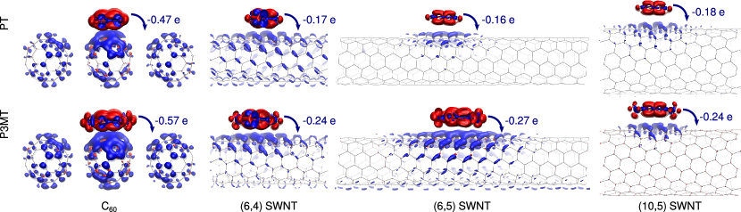
It is useful to consider the spatial distribution of the difference in all electron density between triplet excited state and singlet ground state shown in Figure 1 to determine the origin of these trends in the bulk heterojunctions’ charge transfer. For each bulk heterojunction studied, the hole density is mostly localized on the -bonding highest occupied molecular orbital (HOMO) of PT or P3MT, with the electron density on antibonding levels of the C60 chain or SWNT. Comparing the PT and P3MT bulk heterojunctions, we notice that the hole density clearly extends onto the methyl groups of P3MT. We expect this spatial delocalization of the hole density onto the methyl groups of P3MT makes hole transfer easier in P3MT than PT bulk heterojunctions. For the (6,4), (6,5) and (10,5) SWNT bulk heterojunctions, the electron and hole densities shown in Figure 1 are rather consistent, with the electron density on the upper surface of the SWNT neighboring the PT or P3MT. Conversely, for the C60 chain, the electron density is delocalized over the entire surface of all three fullerenes. This suggests the greater charge transfer onto the C60 chains compared with the SWNTs may have a geometrical origin.
However, although these results clearly demonstrate a charge transfer from donor to acceptor, it remains unclear whether the excited electron and hole are truly free charge carriers or remain bound at the donor/acceptor interface. To address this issue, we provide the zero-bias conductance at the energy of the excited electron and hole in the singlet ground state and triplet excited state in Table 3.
hole carriers electron carriers donor acceptor PT C60 chain 0.0007 0 .003 0.003 0 .02 P3MT C60 chain 0.3 0 .0007 0.09 0 .6 PT (6,4) SWNT 0.05 88 0.02 46 P3MT (6,4) SWNT 0.0005 1 0.01 16 PT (6,5) SWNT 0.0007 0 .007 0.02 0 .005 P3MT (6,5) SWNT 0.0002 0 .01 0.0003 0 .004 PT (10,5) SWNT 0.01 0 .01 0.002 0 .003 P3MT (10,5) SWNT 0.0003 0 .04 0.0002 0 .002
Note that these conductances are across a single fullerene/polymer or SWNT/polymer junction. This is because within the NEGF formalism, the fullerene chain, SWNT, and polymer are all modeled as semi-infinite leads. For this reason, the conductances provided in Table 3 may be considered to be per absorbed photon. Furthermore, because there is only a single PT or P3MT band for this energy range through which current may flow, the quantum of conductance, , provides a theoretical upper bound on the conductance across the junction.
Overall, the conductances quoted in Table 3 vary by over 6 orders of magnitude, from to . Particularly impressive is the (6,4) SWNT/PT junction, with conductances of 9 and 5% of for free hole and electron carriers, respectively. While the (6,4) SWNT junctions clearly provide the highest conductivity in the triplet excited state, the C60 chain/P3MT junction is clearly the most active in the singlet ground state. Comparing the conductance for the junction in the singlet ground state and the triplet excited state, we find that the conductance is generally significantly greater when the system is in the triplet excited state. This suggests that the level hybridization related to the charge transfer observed in Figure 1 facilitates tunnelling across the donor/acceptor gap. However, the opposite is true for the C60 chain/P3MT junction. We also find the (6,5) and (10,5) SWNTs, with their smaller band gaps, have quite low conductivities. This is consistent with recent experimental findings, which showed that (6,5)SWNT/PCBM/P3HT bulk heterojunctions perform rather poorly22.
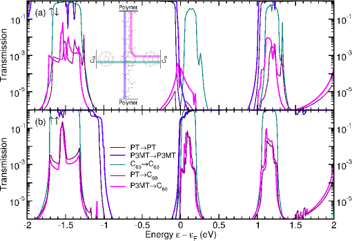
To provide insight into the reasons behind the great variability in the free carrier conductance provided in Table 3 and the origin of the high conductance across the (6,4) SWNT junctions in the triplet excited state, we plot the transmission function near the VBM and CBM for the C60/polymer and SWNT/polymer junctions in Figures 2 and 3, respectively.
For the C60/polymer junction, depicted schematically as an inset in Figure 2(a), we provide the conductance through the polymers (PTPT and P3MTP3MT), along the C60 chain (CC60), and across the junction (PTC60 and P3MTC60). The transmission along the polymers is simply for energies below the HOMO, zero within the energy gap, and above the lowest unoccupied molecular orbital (LUMO). This amounts to a simple counting of the number of bands below the VBM and above the CBM.
In the singlet ground state, the HOMO of PT/P3MT is pinned to the LUMO of C60 at the Fermi level, while in the triplet excited state, the LUMO of PT/P3MT becomes pinned to the LUMO of C60 at the Fermi level of the excited electron . This means any differences in band gap between PT and P3MT do not play an important role for the polymer/fullerene bulk heterojunctions, as the donor HOMO and LUMO are pinned to the LUMO of the acceptor in the ground and excited states, respectively.
Conduction through the C60 chain is rather different. It instead exhibits narrow plateaus centered on the HOMO and LUMO of the C60 chain. As a result, conduction across the polymer/fullerene junction is limited to these narrow plateaus where the C60 chain is conductive, as shown in Figure 2a,b. It is this limitation in the conductivity of C60 chains, which limits their effectiveness within OPV bulk heterojunctions and motivates their replacement with SWNTs21.
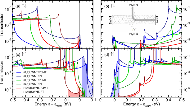
Unlike the C60 chain, the transmission through semiconducting SWNTs exhibits broad plateaus, and is typically below the VBM, zero within the band gap, and above the VBM. As was this case for transmission through the polymers, this amounts to a simple counting of the number of bands below and above the VBM and CBM, respectively. Because the transmission through the polymers and SWNTs is rather trivial, up to scattering due to transmission across the junction, it has been omitted in Figure 3. Instead, we plot the HOMO, singly occupied molecular level (SUMO), singly unoccupied molecular level (SOMO), and LUMO energies below/above which the transmission from PTPT and P3MTP3MT is in Figure 3a–d.
For the SWNT/polymer junctions, we find the conductance is intimately related to the alignment of the SWNT/polymer HOMO and LUMO levels (cf. Figure 3a–d). In fact, the conductance at and depends exponentially on the alignment of the SWNT and polymer HOMOs and LUMOs 55.
For the (6,4) SWNT, with a KS band gap a bit smaller than PT and P3MT, we find both the HOMO and LUMO levels of the polymer and SWNT are aligned in the triplet excited state. Although the resulting charge transfer is rather similar to the other SWNTs studied (cf. Table 2), the improvement in level alignment places and at or near the polymer HOMO and LUMO, respectively. This results in a very high conductivity across the (6,4) SWNT/polymer junctions in the triplet excited state (cf. Table 3). Conversely, the level alignment for the (10,5) SWNT is the poorest of those considered, as the CBM of the nanotube is shifted down relative to the LUMO of the polymer as the band gap decreases.
In fact, if the transmission was measured above or below the polymer LUMO or HOMO, respectively, the conductance across all three polymer/SWNT junctions studied would be % of . This is not the case for the C60 chain, which is only conductive within a narrow range of the chain’s HOMO and LUMO.
Essentially, the conductance across SWNT/polymer heterojunctions can be dramatically improved by a better alignment of the polymer’s HOMO and LUMO levels with the SWNT’s VBM and CBM, respectively. This may be accomplished using a SWNT with a larger band gap, for example, a (6,4) SWNT. However, improving the level alignment too much may lead to a reduction of the electron and hole transfer.
4. CONCLUSIONS
We have employed four descriptors: (1) the triplet state formation energy , (2) the donor to acceptor charge transfer, (3) the conductance of free electron carriers , and (4) the conductance of free hole carriers , to assess the relative performance of OPV bulk heterojunctions with PT and P3MT as donors, and C60 chains, (6,4), (6,5), and (10,5) SWNTs as acceptors. We find P3MT, with its larger band gap, and greater ability to absorb a hole, generally exhibits a greater charge transfer and conductance than PT. The C60 chain accepts significantly more charge ( ) than the SWNTs ( ), which are rather consistent for all SWNTs considered. These results are also consistent with the calculated formation energies for the triplet excited state.
However, the conductance across the junctions via free hole and electron carriers differs by six orders of magnitude among the bulk heterojunctions considered here. In the singlet ground state the C60 chain/P3MT junction has the greatest free hole and electron conductivity of those considered (0.03 and 0.01% of ), while the (6,4) SWNT/PT junction shows a dramatic increase in conductivity in the triplet excited state (9 and 5%). This suggests that by improving the level alignment of the polymer and SWNT through the use of larger band gap SWNTs one may obtain a dramatic improvement in OPV efficiency.
Altogether, these results demonstrate the importance of considering the hybridization of donor/acceptor levels in the excited state, and the resulting dependence on level alignment of the conductivity. This dramatic dependence on the level alignment observed herein provides significant motivation for future studies including the dependence on the vibrational modes of the molecules27, and more advanced quasiparticle calculations including anisotropic screening effects56, 57, 58, 59, 60 in the polymer/SWNT level alignment. Furthermore, a reformulation of the NEGF method to describe photoinduced quantum transport is required to describe the optical absorption-dependent photovoltaic efficiency of OPV devices. The techniques employed herein provide a roadmap for the computational design of OPV bulk heterojunctions in silico.
AUTHOR INFORMATION
Corresponding Author
*E-mail: duncan.mowbray@gmail.com. Tel: +34 943 01 8392.
Notes
The authors declare no competing financial interest.
ACKNOWLEDGMENTS
The authors thank Angel Rubio and Lluís Blancafort for fruitful discussions. We acknowledge financial support from the European Projects POCAONTAS (FP7-PEOPLE-2012-ITN-316633), DYNamo (ERC-2010-AdG-267374), MOSTOPHOS (SEP-210187476), and EUSpec (COST Action MP1306); Spanish Grants (FIS20113-46159-C3-1-P) and “Grupos Consolidados UPV/EHU del Gobierno Vasco” (IT-578-13); the Air Force Office of Scientific Research (AFOSR) (FA2386-15-1-0006 AOARD 144088); and computational time from the BSC Red Espanola de Supercomputacion.
REFERENCES
- 1 U.S. Department of Energy. Photovoltaic Cell Conversion Efficiency Basics. http://energy.gov/eere/energybasics/articles/photovoltaic- cell-conversion-efficiency-basics (accessed Aug 20, 2013).
- 2 U.S. Department of Energy. Photovoltaic Cell Quantum Efficiency Basics. http://energy.gov/eere/energybasics/articles/photovoltaic- cell-quantum-efficiency-basics (accessed Aug 20, 2013).
- Ando 1997 Ando, T. Excitons in Carbon Nanotubes. J. Phys. Soc. Jap. 1997, 66, 1066–1073
- Perebeinos et al. 2004 Perebeinos, V.; Tersoff, J.; Avouris, P. Scaling of Excitons in Carbon Nanotubes. Phys. Rev. Lett. 2004, 92, 257402
- Spataru et al. 2004 Spataru, C. D.; Ismail-Beigi, S.; Benedict, L. X.; Louie, S. G. Excitonic Effects and Optical Spectra of Single-Walled Carbon Nanotubes. Phys. Rev. Lett. 2004, 92, 077402
- Wang et al. 2005 Wang, F.; Dukovic, G.; Brus, L. E.; Heinz, T. F. The Optical Resonances in Carbon Nanotubes Arise from Excitons. Science 2005, 308, 838–841
- Maultzsch et al. 2005 Maultzsch, J.; Pomraenke, R.; Reich, S.; Chang, E.; Prezzi, D.; Ruini, A.; Molinari, E.; Strano, M. S.; Thomsen, C.; Lienau, C. Exciton Binding Energies in Carbon Nanotubes from Two-Photon Photoluminescence. Phys. Rev. B: Condens. Matter Mater. Phys. 2005, 72, 241402
- Kanai and Grossman 2007 Kanai, Y.; Grossman, J. C. Insights on Interfacial Charge Transfer Across P3HT/Fullerene Photovoltaic Heterojunction from Ab Initio Calculations. Nano Lett. 2007, 7, 1967–1972
- Kanai and Grossman 2008 Kanai, Y.; Grossman, J. C. Role of Semiconducting and Metallic Tubes in P3HT/Carbon-Nanotube Photovoltaic Heterojunctions: Density Functional Theory Calculations. Nano Lett. 2008, 8, 908–912
- Holt et al. 2010 Holt, J. M.; Ferguson, A. J.; Kopidakis, N.; Larsen, B. A.; Bult, J.; Rumbles, G.; Blackburn, J. L. Prolonging Charge Separation in P3HT–SWNT Composites Using Highly Enriched Semiconducting Nanotubes. Nano Lett. 2010, 10, 4627–4633
- Jain et al. 2012 Jain, R. M.; Howden, R.; Tvrdy, K.; Shimizu, S.; Hilmer, A. J.; McNicholas, T. P.; Gleason, K. K.; Strano, M. S. Polymer-Free Near-Infrared Photovoltaics with Single Chirality (6,5) Semiconducting Carbon Nanotube Active Layers. Adv. Mater. 2012, 24, 4436–4439
- Mallajosyula et al. 2008 Mallajosyula, A.; Iyer, S. S. K.; Mazhari, B. Conduction properties of carbon nanotubes in P3HT:SWNT bulk heterojunction solar cells. IEEE Photovoltaic Spec. Conf., 33rd 2008, 1–6
- Ferguson et al. 2013 Ferguson, A. J.; Blackburn, J. L.; Kopidakis, N. Fullerenes and Carbon Nanotubes as Acceptor Materials in Organic Photovoltaics. Mater. Lett. 2013, 90, 115–125
- Kymakis and Amaratunga 2002 Kymakis, E.; Amaratunga, G. A. J. Single-Wall Carbon Nanotube/Conjugated Polymer Photovoltaic Devices. Appl. Phys. Lett. 2002, 80, 112–114
- Kymakis et al. 2003 Kymakis, E.; Alexandrou, I.; Amaratunga, G. A. J. High Open-Circuit Voltage Photovoltaic Devices from Carbon-Nanotube-Polymer Composites. J. Appl. Phys. 2003, 93, 1764–1768
- Stich et al. 2013 Stich, D.; Späth, F.; Kraus, H.; Sperlich, A.; Dyakonov, V.; Hertel, T. Triplet-Triplet Exciton Dynamics in Single-Walled Carbon Nanotubes. Nat. Photonics 2013, 8, 139–144
- Bindl et al. 2011 Bindl, D. J.; Wu, M.-Y.; Prehn, F. C.; Arnold, M. S. Efficiently Harvesting Excitons from Electronic Type-Controlled Semiconducting Carbon Nanotube Films. Nano Lett. 2011, 11, 455–460
- Bindl et al. 2013 Bindl, D. J.; Ferguson, A. J.; Wu, M.-Y.; Kopidakis, N.; Blackburn, J. L.; Arnold, M. S. Free Carrier Generation and Recombination in Polymer-Wrapped Semiconducting Carbon Nanotube Films and Heterojunctions. J. Phys. Chem. Lett. 2013, 4, 3550–3559
- Bindl and Arnold 2013 Bindl, D. J.; Arnold, M. S. Efficient Exciton Relaxation and Charge Generation in Nearly Monochiral (7,5) Carbon Nanotube/C60 Thin-Film Photovoltaics. J. Phys. Chem. C 2013, 117, 2390–2395
- Lan and Li 2013 Lan, F.; Li, G. Direct Observation of Hole Transfer from Semiconducting Polymer to Carbon Nanotubes. Nano Lett. 2013, 13, 2086–2091
- Goutam et al. 2012 Goutam, P. J.; Singh, D. K.; Iyer, P. K. Photoluminescence Quenching of Poly(3-hexylthiophene) by Carbon Nanotubes. J. Phys. Chem. C 2012, 116, 8196–8201
- Gomulya et al. 2013 Gomulya, W.; Gao, J.; Loi, M. A. Conjugated Polymer-Wrapped Carbon Nanotubes: Physical Properties and Device Applications. Eur. Phys. J. B 2013, 86, 404
- Lanzi et al. 2008 Lanzi, M.; Paganin, L.; Caretti, D. New Photoactive Oligo- and Poly-Alkylthiophenes. Polymer 2008, 49, 4942–4948
- Vardeny et al. 1987 Vardeny, Z.; Ehrenfreund, E.; Shinar, J.; Wudl, F. Photoexcitation Spectroscopy of Polythiophene. Phys. Rev. B: Condens. Matter Mater. Phys. 1987, 35, 2498–2500
- Ren-Kuan et al. 1988 Ren-Kuan, Y.; Zhen-Chun, H.; You-Dou, Z.; Wen-Guo, T.; Zi-Yuan, L.; Xue-Chu, S. Photoluminescence of Poly(3-methyl thiophene)–P3MT. Acta Phys. Sin. 1988, 37, 857
- Bachilo et al. 2002 Bachilo, S. M.; Strano, M. S.; Kittrell, C.; Hauge, R. H.; Smalley, R. E.; Weisman, R. B. Structure-Assigned Optical Spectra of Single-Walled Carbon Nanotubes. Science 2002, 298, 2361
- Galperin and Nitzan 2011 Galperin, M.; Nitzan, A. Raman Scattering and Electronic Heating in Molecular Conduction Junctions. J. Phys. Chem. Lett. 2011, 2, 2110–2113
- Le Bahers et al. 2011 Le Bahers, T.; Labat, F.; Pauporté, T.; Lainé, P. P.; Ciofini, I. Theoretical Procedure for Optimizing Dye-Sensitized Solar Cells: From Electronic Structure to Photovoltaic Efficiency. J. Am. Chem. Soc. 2011, 133, 8005–8013
- Labat et al. 2012 Labat, F.; Le Bahers, T.; Ciofini, I.; Adamo, C. First-Principles Modeling of Dye-Sensitized Solar Cells: Challenges and Perspectives. Acc. Chem. Res. 2012, 45, 1268–1277
- Le Bahers et al. 2013 Le Bahers, T.; Pauporté, T.; Lainé, P.; Labat, F.; Adamo, C.; Ciofini, I. Modeling Dye-Sensitized Solar Cells: From Theory to Experiment. J. Phys. Chem. Lett. 2013, 4, 1044–1050
- Bader 1990 Bader, R. F. W. Atoms in Molecules: A Quantum Theory; Oxford University, 1990; Vol. 3; pp 1–120
- Mowbray et al. 2009 Mowbray, D. J.; Morgan, C.; Thygesen, K. S. Influence of O2 and N2 on the Conductivity of Carbon Nanotube Networks. Phys. Rev. B: Condens. Matter Mater. Phys. 2009, 79, 195431
- Meir and Wingreen 1992 Meir, Y.; Wingreen, N. S. Landauer Formula for the Current Through an Interacting Electron Region. Phys. Rev. Lett 1992, 68, 2512–2515
- Datta 1997 Datta, S. Electronic Transport in Mesoscopic Systems, 1st ed.; Cambridge University Press: Cambridge, 1997
- Thygesen and Jacobsen 2005 Thygesen, K.; Jacobsen, K. Molecular Transport Calculations with Wannier Functions. Chem. Phys. 2005, 319, 111–125
- Thygesen 2006 Thygesen, K. S. Electron Transport Through an Interacting Region: The Case of a Nonorthogonal Basis Set. Phys. Rev. B: Condens. Matter Mater. Phys. 2006, 73, 035309
- Harris 1999 Harris, P. J. F. Carbon Nanotubes and Related Structures: New Materials for the Twenty-first Century; Cambridge University Press: Cambridge, 1999
- Dresselhaus et al. 2001 Dresselhaus, M. S., Dresselhaus, G., Avouris, P., Eds. Carbon Nanotubes: Synthesis, Structure, Properties, and Applications; Springer: Berlin, 2001
- García-Lastra et al. 2008 García-Lastra, J. M.; Thygesen, K. S.; Strange, M.; Rubio, Á. Conductance of Sidewall-Functionalized Carbon Nanotubes: Universal Dependence on Adsorption Sites. Phys. Rev. Lett. 2008, 101, 236806
- García-Lastra et al. 2010 García-Lastra, J. M.; Mowbray, D. J.; Thygesen, K. S.; Rubio, Á.; Jacobsen, K. W. Modeling Nanoscale Gas Sensors Under Realistic Conditions: Computational Screening of Metal-Doped Carbon Nanotubes. Phys. Rev. B: Condens. Matter Mater. Phys. 2010, 81, 245429
- Mortensen et al. 2005 Mortensen, J. J.; Hansen, L. B.; Jacobsen, K. W. Real-Space Grid Implementation of the Projector Augmented Wave Method. Phys. Rev. B: Condens. Matter Mater. Phys. 2005, 71, 035109
- Enkovaara et al. 2010 Enkovaara, J. et al. Electronic Structure Calculations with GPAW: A Real-Space Implementation of the Projector Augmented-Wave Method. J. Phys.: Condens. Matter 2010, 22, 253202
- Larsen et al. 2009 Larsen, A. H.; Vanin, M.; Mortensen, J. J.; Thygesen, K. S.; Jacobsen, K. W. Localized Atomic Basis Set in the Projector Augmented Wave Method. Phys. Rev. B: Condens. Matter Mater. Phys. 2009, 80, 195112
- Perdew et al. 1996 Perdew, J. P.; Burke, K.; Ernzerhof, M. Generalized Gradient Approximation Made Simple. Phys. Rev. Lett. 1996, 77, 3865
- Strange et al. 2008 Strange, M.; Kristensen, I. S.; Thygesen, K. S.; Jacobsen, K. W. Benchmark Density Functional Theory Calculations for Nanoscale Conductance. J. Chem. Phys. 2008, 128, 114714
- Mowbray 2014 Mowbray, D. J. Theoretical Electron Energy Loss Spectroscopy of Isolated Graphene. Phys. Stat. Solidi B 2014, 251, 2509–2514
- Glanzmann et al. 2015 Glanzmann, L. N.; Mowbray, D. J.; Figueroa del Valle, D. G.; Scotognella, F.; Lanzani, G.; Rubio, A. Photoinduced Absorption within Single-Walled Carbon Nanotube Systems. J. Phys. Chem. C 2015, 120, 1926–1935
- Glanzmann et al. 2014 Glanzmann, L. N.; Mowbray, D. J.; Rubio, A. PFO-BPy Solubilizers for SWNTs: Modelling Polymers from Oligomers. Phys. Stat. Solidi B 2014, 251, 2407–2412
- Bahn and Jacobsen 2002 Bahn, S. R.; Jacobsen, K. W. An Object-Oriented Scripting Interface to a Legacy Electronic Structure Code. Comput. Sci. Eng. 2002, 4, 56
- Cumings and Zettl 2005 Cumings, J.; Zettl, A. In Applied Physics of Carbon Nanotubes; Fundamentals of Theory, Optics, and Transport Devices; Rotkin, S. V., Subramoney, S., Eds.; Springer-Verlag: Berlin, 2005; pp 273–306
- Kelly et al. 1992 Kelly, M. K.; Etchegoin, P.; Fuchs, D.; Krätschmer, W.; Fostiropoulos, K. Optical Transitions of Films in the Visible and Ultraviolet from Spectroscopic Ellipsometry. Phys. Rev. B: Condens. Matter Mater. Phys. 1992, 46, 4963–4968
- Grüneis et al. 2008 Grüneis, A.; Attaccalite, C.; Wirtz, L.; Shiozawa, H.; Saito, R.; Pichler, T.; Rubio, A. Tight–Binding Description of the Quasiparticle Dispersion of Graphite and Few–Layer Graphene. Phys. Rev. B: Condens. Matter Mater. Phys. 2008, 78, 205425
- Umari et al. 2012 Umari, P.; Petrenko, O.; Taioli, S.; De Souza, M. M. Communication: Electronic Band Gaps of Semiconducting Zig-Zag Carbon Nanotubes from Many-Body Perturbation Theory Calculations. J. Chem. Phys. 2012, 136, 181101
- Despoja and Mowbray 2014 Despoja, V.; Mowbray, D. J. Using Surface Plasmonics to Turn on Fullerene’s Dark Excitons. Phys. Rev. B: Condens. Matter Mater. Phys. 2014, 89, 195433
- Mowbray et al. 2008 Mowbray, D. J.; Jones, G.; Thygesen, K. S. Influence of Functional Groups on Charge Transport in Molecular Junctions. J. Chem. Phys. 2008, 128, 111103
- Migani et al. 2013 Migani, A.; Mowbray, D. J.; Iacomino, A.; Zhao, J.; Petek, H.; Rubio, A. Level Alignment of a Prototypical Photocatalytic System: Methanol on TiO2(110). J. Am. Chem. Soc. 2013, 135, 11429–11432
- Migani et al. 2014 Migani, A.; Mowbray, D. J.; Zhao, J.; Petek, H.; Rubio, A. Quasiparticle Level Alignment for Photocatalytic Interfaces. J. Chem. Theory Comput. 2014, 10, 2103–2114
- Migani et al. 2015 Migani, A.; Mowbray, D. J.; Zhao, J.; Petek, H. Quasiparticle Interfacial Level Alignment of Highly Hybridized Frontier Levels: H2O on TiO2(110). J. Chem. Theory Comput. 2015, 11, 239–251
- Sun et al. 2015 Sun, H.; Mowbray, D. J.; Migani, A.; Zhao, J.; Petek, H.; Rubio, A. Comparing Quasiparticle H2O Level Alignment on Anatase and Rutile TiO2. ACS Catal. 2015, 5, 4242–4254
- Mowbray and Migani 2015 Mowbray, D. J.; Migani, A. Using Level Alignment to Identify Catechol’s Structure on TiO2(110). J. Phys. Chem. C 2015, 119, 19634–19641