Multiple negative differential conductance regions and inelastic phonon assisted tunneling in graphene-hBN-graphene structures
Abstract
In this paper we study in detail the effect of the rotational alignment between a hexagonal boron nitride (hBN) slab and the graphene layers in the vertical current of a a graphene-hBN-graphene device. We show how for small rotational angles, the transference of momentum by the hBN crystal lattice leads to multiple peaks in the I-V curve of the device, giving origin to multiple regions displaying negative differential conductance. We also study the effect of scattering by phonons in the vertical current an see how the opening up of inelastic tunneling events allowed by spontaneous emission of optical phonons leads to sharp peaks in the second derivative of the current.
I Introduction
Being able to tailor the properties of materials at will, aiming at unveiling new physics and achieving never though before properties, is the main goal of condensed matter physics and materials science. However, the degree of manipulation we can undertake using conventional materials is somewhat limited. In the last ten years, the advent of two-dimensional materials Novoselov et al. (2004, 2005) opened new avenues waiting for being explored. One of the less explored avenue is the one opened by van der Waals (vdW) hybrid structuresPonomarenko L. A. et al. (2011), new systems formed by stacking layers of two-dimensional crystals on top of each other, have emerged as a new approach for manipulating and tailoring material properties at willNovoselov and Neto (2012); Geim A. K. and Grigorieva I. V. . Among the various possible combinations of two dimensional crystals, graphene - semiconductor/insulator - graphene vdW structures, with semiconducting transition metal dichalcogenide (STMDC) or hexagonal boron nitride (hBN) as the semiconductor/insulator, have emerged as some of the most promising from the point of view of applications. The possibility of controlling electrostatically the effective barrier height presented by the insulator/semiconductor to the vertical flow of electrons between the two graphene layers with a gate voltage has enabled the operation these devices as transistorsBritnell et al. (2012a, b); Georgiou Thanasis et al. (2013), with ON/OFF ratios as high as being possible in graphene-WS2-graphene devicesGeorgiou Thanasis et al. (2013). It was also shown that graphene-STMDC-graphene devices can operate as photodectectors with high quantum efficiencies and fast response times Britnell et al. (2013); Yu Woo Jong et al. (2013); Massicotte et al. (2016). Due to the extreme high quality and atomically sharp interfaces Haigh et al. (2012) between different layers in vdW structures , lattice mismatch and relative alignment between consecutive layers play a fundamental role in determining the electronic coupling between different layers of the vdW structure, ultimately determining its electronic and optical properties. Lattice misalignment between different layers has been known to lead to the formation of Moir patterns in rotated graphite layers Pong and Durkan (2005). The effect of lattice misalignment and mismatch has been extensively studied in the context of twisted graphene bilayers and graphene-on-hBN structures. It was shown theoretically and experimentally, that misalignment in a graphene bilayer leads to a renormalization of graphene’s Fermi velocity Lopes dos Santos et al. (2007); Luican et al. (2011). It was also found out that mismatch and misalignment controls the formation of mini Dirac cones in the band structure of graphene - hBN structures systems Park et al. (2008); Yankowitz et al. (2012); Ortix et al. (2012); Wallbank et al. (2013); Mucha-Kruczyński et al. (2013); Ponomarenko et al. (2013)..
The dependence of the vertical current in vdW structures on the rotation between different layers was first studied in Ref. Bistritzer and MacDonald, 2010 in the context of twisted bilayer graphene, where it was found that the current is extremely sensitive to the twist angle. Although this dependence was not at first completely appreciated, it was soon understood and verified Mishchenko et al. (2014); Brey (2014) that the misalignment between the graphene layers in graphene-hBN-graphene structures can lead to the occurrence of negative differential conductance (NDC) regions, with the I-V curve displaying peaks whose dependence on the bias voltage depends on the rotation angle between the graphene layers. More recently, the effect of misalignment on the vertical current in devices formed by two graphene bilayers Fallahazad et al. (2015); Kang et al. (2015); de la Barrera and Feenstra (2015) and by one graphene monolayer and a graphene bilayer separated by hBN has also been studied.Lane et al. (2015) Scattering by phonons can lead to incoherent phonon assisted tunneling between the graphene layers. This effect has been first theoretically studied for vdW structures for twisted graphene bilayers Perebeinos et al. (2012). More recently, effects of phonon assisted scattering on vertical transport have been experimentally detected in graphene-hBN-graphite Jung et al. (2015) and graphene-hBN-graphene structures Vdovin et al. (2015) and have been proposed as a possible way to probe the phonon spectrum of vdW structures.
In this paper we describe the vertical current in graphene-hBN-graphene devices with misaligned layers, and for small twist angles, properly taking into account momentum conservation rules, within the non-equilibrium Green’s function framework and using a tight-binding based continuous Hamiltonian. We show that the present theory reduces to the ones used in Refs. Brey, 2014; Mishchenko et al., 2014. By taking into account processes involving transference of momentum by the hBN crystal lattice to the tunneling electrons, we find that the vertical current depends sensitively on the relative alignment between the graphene layers and the hBN slab and that by carefully controlling this alignment, it is possible to obtain several peaks in the I-V curve of the device, followed by regions of NDC, a possibility that has not been considered previously. We also find out that the structure of graphene wavefunctions manifests itself in the vertical current, suppressing some of the current peaks that would be expected with considerations based only on electronic dispersion relations. We study the effect of resonant disorder in the graphene layers in the vertical current, treated within the self-consistent Born approximation (SCBA) which correctly describes the proportionality of the transport lifetime with the energyPeres (2010). We finally study how phonons and disorder give origin to non-coherent current between the two graphene layers, deriving an expression for it.
The paper is organized as follows. In Sec. II we describe the theoretical framework we employed in this work: in subsection II.1, we present the Hamiltonian used to model the graphene-hBN-graphene device and in subsection II.2 we present the fundamental equations used to treat transport within the non-equilibrium Green’s functions formalism. In Sec. III we discuss the coherent tunneling flowing through a pristine device taking into account the lattice mismatch and misalignment between graphene layers and the hBN slab. The consequences of treating graphene as part of the device or as external contacts are discussed and the role of the momentum transferred to the tunneling electrons by the hBN lattice is analyzed in detail. The effect of an in-plane magnetic field in the current is also discussed. In Sec. IV, the effects of disorder and phonon scattering into the vertical current are studied and a expression for the phonon/disorder assisted current to lowest order in perturbation theory is derived. Finally, in Sec. V we conclude. Technical details and longer derivations are include as Appendices.
II Formalism
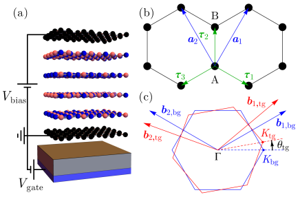
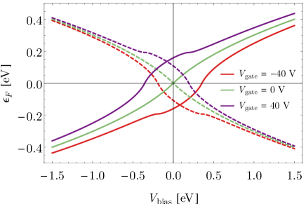
We want to study the vertical current flowing through a device formed by two graphene layers (bottom, bg, and top, tg) separated by a few layers, , of hBN. The distance between the two graphene layers is given by . We assume that the top graphene layer and the hBN slab are rotated with respect to the bottom graphene layer by an angle of and , respectively. We assume that layers forming the hBN slab are perfectly aligned with an stackingGeick et al. (1966); Ribeiro and Peres (2011) (consecutive honeycomb lattices are perfectly aligned, with each boron/nitrogen atom of one layer directly on top of the nitrogen/atom of the next layer). A bias voltage, , can be applied between the top and bottom graphene layers, which will induce a current between the two. The doping of the graphene layers can be controlled by application of a gate voltage to the bottom graphene. A schematic of the typical device structure is shown in Fig. 1.
II.1 Model Hamiltonian
We model the graphene - hBN - graphene system with the following Hamiltonian
| (1) |
where is the Hamiltonian describing the isolated bottom/top graphene layer and describes the hopping of electrons from the bottom/top graphene layer to the hBN slab. The current between the two graphene layers will be dominated by low energy states. Focusing on the states close to the and points of the bottom graphene layer, we write the Hamiltonian of the bottom graphene layer in sublattice basis and in term of Bloch states as the massless Dirac Hamiltonian
| (2) |
where is graphene’s Fermi velocity, is a on-site potential induced by the applied bias and gate voltages, is the electron creation operator for states localized in the A/B sublattice, in the valley (), with momentum (measured from the Brillouin zone center) and is the angle formed between and . We choose the zero of energy to lie at the Fermi level of the bottom graphene layer, in which case we have , where is the Fermi energy of the bottom graphene layer measured from its Dirac point. The Hamiltonian in Eq. (2) is diagonalized by the eigenstates with corresponding dispersion relation , with for electrons in the conduction/valence band. Since we will be interested in studying the vertical current to lowest order in the graphene-hBN coupling, we neglect the effect of the periodic potential generated by the hBN slab in dispersion relation of graphene electronic states Park et al. (2008); Yankowitz et al. (2012); Kindermann et al. (2012); Ortix et al. (2012); Wallbank et al. (2013); Mucha-Kruczyński et al. (2013); Jung et al. (2014). Using the same reference frame in momentum space as in Eq. (2), the Hamiltonian describing the top graphene layer in the Dirac cone approximation reads
| (3) |
where , is measured from the point of the top graphene layer, with ( a rotation matrix), is the displacement between the Dirac points of the two rotated graphene layers and is measured with respect to the Dirac point of the bottom graphene graphene layer. is the angle between and and is an on-site potential, due to the applied bias and gate voltages, and is given by , with the Fermi level of the top graphene layer measured from its Dirac point and the fundamental electronic charge. The remaining symbols in Eq. (3) are similarly defined to the ones in Eq. (2). Due to the large band gap of boron nitride, we ignore its momentum dependence, writing the hBN slab Hamiltonian as
| (4) |
where creates an electron in layer of the hBN slab, in the boron (B)/nitrogen (N) site, specifies the valley, and are, respectively, the on-site energies of boron and nitride sites measured from the Dirac point of graphene, is the nearest neighbour interlayer hoping and is a potential induced by the applied voltages. Due to the large energy offset between graphene and hBN sites, the charge accumulated in the hBN layers will be negligible. In this case a simple electrostatic calculation (see Appendix A) gives us . For two rotated crystal layers, Bloch states from different layers can only be coupled provided momentum is conserved modulo any combination of reciprocal lattice vectors of both layers Bistritzer and MacDonald (2010); Koshino (2015), in a so called generalized Umklapp process. Focusing on low energy states and considering only the three most relevant processes, the coupling between the graphene layers and the hBN slab is described by (see Appendix B)
| (5) |
where is an annihilation operator of an electron in the graphene layer with momentum measured from the point, is a creation operator of an electron state in the layer of the hBN slab, with momentum measured from , and with the matrices and defined as
| (8) | |||||
| (11) |
where () is the hoping parameter between a carbon site and boron (nitrogen) site and the vectors are given by (see Appendix B)
| (12) | |||||
| (13) | |||||
| (14) |
where and () are, respectively, the reciprocal lattice vectors of the bottom/top graphene layer and of the hBN slab (see Fig. 1). Notice that if the boron nitride slab is formed by an even number of layers, one must replace for , since boron and nitrogen atoms switch positions in consecutive layers of hBN. Different reciprocal lattice vectors are related to each other by and , where is a scale factor, with () the lattice parameter of graphene (hBN). Hamiltonians of the form of Eq. (5) have previously been used to study twisted graphene bilayers Lopes dos Santos et al. (2007); Bistritzer and MacDonald (2011); Lopes dos Santos et al. (2012); Moon and Koshino (2013) and graphene-on-hBN structures Kindermann et al. (2012); Jung et al. (2014); Moon and Koshino (2014). Considering the three processes coupling the bottom graphene with hBN and the three processes connecting hBN to the top graphene layer, described by Eq. (5), there are nine hBN mediated processes coupling the bottom graphene layer to the top one Brey (2014). These nine processes couple a state from the bottom graphene layer with momentum (measured from ) to states of the top graphene layer with momentum (measured from ) with (see Appendix B)
| (15) |
The processes with involve transfer of momentum by the hBN lattice, while processes with do not. At zero magnetic field, the overall three-fold rotational invariance of the graphene-hBN-graphene structure implies that these nine processes can be organized in three groups of three, with processes in the same group being related by rotation and therefore giving the same contribution to the vertical current. The three groups are
| (16) | |||
with length of the vectors in each group being the same. For small rotation angles and lattice mismatch, , we have 111In Ref. Brey, 2014, the processes corresponding to and where identified as being equivalent, with . This was likely caused by first expanding to linear order in , and , and only then evaluating , loosing in the process terms involving the product in , which lift the equivalence between the processes associated with and .
| (17) | |||||
| (18) | |||||
| (19) |
with the length of .
II.2 Current evaluation
The standard approach to transport in a mesoscopic device assumes that the device is attached to external contacts that are in a thermal equilibrium state with well defined chemical potentials. This is only an approximation as once a current starts flowing through the system, the contacts will also be in a non-equilibrium state Frensley (1990); Vogl and Kubis (2010). The problem of computing the current flowing through a mesoscopic device is then analogous to the problem of computing the water flux through a thin pipe that is connecting two large vessels with different water levels Stone and Szafer (1988). Once water starts flowing through the pipe, the water levels in each vessel are no longer constants, however, on short time scales, assuming that the water levels in the vessels are constant is a reasonable approximation, provided that these are wide enough with respect to the pipe. In the same way, within short time scales compared to the depletion time of an external battery, it is a reasonable approximation to assume that the external contacts have well defined, constant chemical potentials. Using the non-equilibrium Green’s function technique one can then show that in a mesoscopic device that is attached to two non-interacting222In mesoscopic transport, the problem of computing the current that is flowing through the device is reduced to a problem only involving degrees of freedom in the mesoscopic region by integrating out the external contacts. This is only done exactly provided the contacts are non-interacting. contacts, bottom and top, in thermal equilibrium state described, respectively, by the Fermi-Dirac distribution functions and with the chemical potential of the bottom (top) contact, the current flowing from the bottom to the top contact is given by Haug and Jauho (2008) (using a compact notation where a capital bold face symbols represent matrix elements evaluated in some one-particle electron basis and omitting the frequency argument of the different quantities)
| (20) | |||||
with the spectral function of the central mesoscopic device given by
| (21) | |||||
where is the retarded/advanced/lesser/greater Green’s function of the central device (which takes into account coupling to the external contacts) and is a level width function due to the bottom (top) contact. The level width function is the density of states of the contacts weighted by the their coupling to the central device: , with the Hamiltonian describing the bottom (top) contact and describing the coupling between the central device and the contact. The second equality in Eq. (21) is true by the very definition of the different Green’s functions. A property that will latter be useful isDatta (1997)
| (22) | |||||
where the decay rate matrix is defined as . This result can be obtained by writing
| (23) | |||||
Using the Dyson equation for the retarded/advanced Green’s function, , with indicating the bare Green’s function (in the absence of interactions and coupling to external contacts), and nothing that and only differ by an infinitesimal constant that is taken to zero, the decay rate matrix can be written as
| (24) | |||||
where the last identity is inherited from the second equality in Eq. (21). The lesser/greater Green’s functions obey the Keldysh equation Haug and Jauho (2008)
| (25) |
where the lesser/greater self-energy can be split into contributions from the contacts and interactions as
| (26) | |||||
| (27) |
with the contribution from interactions. In the same manner, the decay rate Eq. (24) can be split into a contribution from external contacts and interactions
| (28) |
Using Eqs. (22) and (25)-(28) in Eq. (20), the total current can then be written as a sum of coherent and incoherent contributions
| (29) |
with the coherent contribution being given by the Landauer formula
| (30) |
with the transmission function given by
| (31) |
and the incoherent contribution, which describes sequential tunneling processes and plays the same role as vertex corrections in the Kubo formalism for linear response, being given by
| (32) |
In the following sections we will use these general formalism together with the model Hamiltonian from Sec. II.1 to evaluate the vertical current in graphene-hBN-graphene structures.
III Current in the non-interacting, pristine limit
III.1 General discussion
When applying the non-equilibrium Green’s function formalism to a graphene-hBN-graphene device with metal contacts, one is faced with the issue of how to make the separation between central mesoscopic region, and the external contacts which are in thermal equilibrium. Two natural approaches exist: (A) describing the graphene layers as part of the external contacts, and (B) describing the graphene layers as part of the central mesoscopic device. In all theoretical analytic works to date, the graphene layers were assumed to be part of the external contacts Feenstra et al. (2012); Vasko (2013); Brey (2014); Mishchenko et al. (2014); de la Barrera and Feenstra (2015), being in equilibrium. However, due to the low density of states of graphene, it seems more natural to consider graphene as part of the mesoscopic device. We will start from approach (B) and see that under certain approximations, it reduces to approach (A). We will first consider the non-interacting, pristine case. In approach (B), in Eq. (31) is the Green’s function of the graphene-hBN-graphene device. We are interested in the matrix elements of that connect the bottom and the top contacts. Due to the block diagonal structure of the Hamiltonian (1) (there is no direct coupling between the two graphene layers), these can generally be written as
| (33) | |||||
| (34) |
where are the Green’s function of the bottom/top graphene layer in the absence of graphene-hBN coupling (but tacking into account coupling to the external contacts) where we have defined the hBN mediated tunneling amplitudes
| (35) | |||||
| (36) |
with the Green’s function of the hBN slab, which in general takes into account its coupling to the graphene layers. Therefore, the transmission function Eq. (31) can be written as
| (37) | |||||
If we now use Eq. (22), we can write the spectral function of the bottom graphene layer taking into account the coupling to the bottom metallic contact, , as and similarly for the top graphene layer. As such, the transmission function can be written as
| (38) |
Eq. (38) is the result that would be directly obtained, if we followed approach (A) instead, in which case the level width functions are given by and . As such we have proved that in the non-interacting case both approaches (A) and (B) coincide. We will leave the discussion for tunneling in the presence disorder and electron-phonon interactions to the next section.
In order to make analytic progress, we will employ the wide-band limit for the metallic contacts, neglecting any frequency dependence of , and assume that the contacts couple equally to all graphene states, not spoiling translation invariance. We expect that this last approximation works well for cases where the metallic contacts are deposited on a small region of the graphene sample. Within these approximations, the only effect of the metallic contacts is to introduce a broadening factor of in the Green’s function of the bottom/top graphene layer. We will now write for a graphene-hBN-graphene device more explicitly. Using the graphene-hBN coupling Hamiltonian Eq. (5), the transmission function can be written using the Bloch momentum basis as (writing explicitly the frequency argument)
| (39) |
with the sum on going from to and where and are measured from the position of the Dirac point in the bottom and top graphene layers, respectively. The effective tunneling probability can be written as
| (40) |
where , with , are graphene wavefunction overlap factors and
| (41) |
with the trace being performed over the sublattice degrees of freedom. Neglecting the frequency dependence of and to lowest order in we can write
| (42) |
Notice, that in Eq. (39) both valleys give the same contribution, which can be seen by making a simultaneous change and . The transmission function can then be written as
| (43) |
where is the area of the device, are the spin and valley degeneracies and we have defined the tunneling density of states as
| (44) |
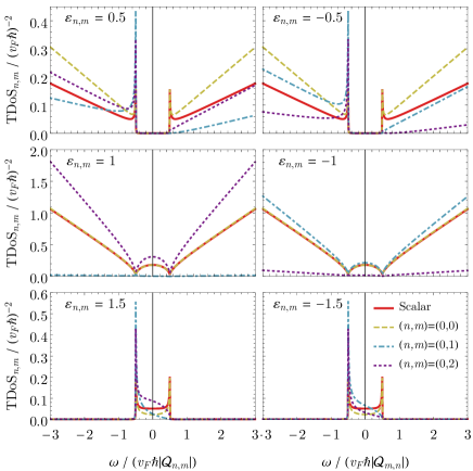
which only depends of the graphene’s dispersion relation and wavefunctions (for simplicity we have dropped the valley indice ). In the limit of infinite lifetime for graphene electrons, the spectral functions reduce to -functions and it is possible to provide an analytic expression for . In the presence of a finite, momentum independent, lifetime, it is still possible to find an approximate analytic expression to Eq. (44). These analytic expressions lead to a significant speed up in the evaluation of the current and are presented in Appendix C. The presence of the spectral functions for the bottom and top graphene layers leads to conservation of energy and momentum in the tunneling process between the two graphene layers.
III.2 Results
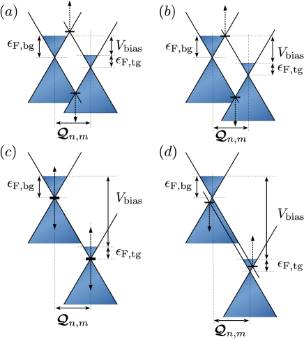
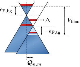
The tunneling in a graphene-hBN-graphene structure is controlled both by energy-momentum conservation and by Pauli’s exclusion principle. The constrains imposed by energy-momentum conservation can be understood considering that the Dirac cones of the bottom and top graphene layers are shifted in energy by a value of and in momentum by a value of , see Fig. 3. The intersection of the shifted cones allows one to visualize the states which respect energy-momentum conservationBrey (2014). Whenever the bias voltage is tuned such that
| (45) |
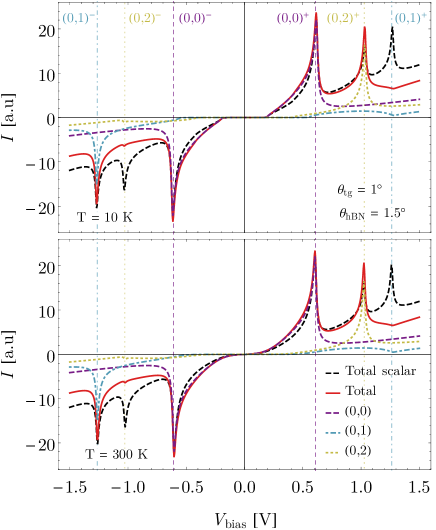
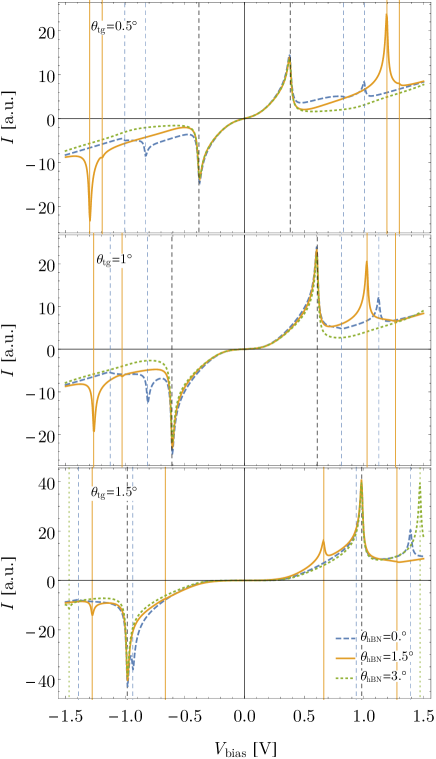
there is a complete overlap of the Dirac cones and a maximum in the current occurs. The information regarding energy-momentum conservation for an electron tunneling between the two graphene layers is encoded in the the function. In Fig. 2 we plot the quantity , for different values of . For , the tunneling is due to intraband processes (from the conduction/valence band of the bottom graphene into the conduction/valence band of the top graphene), going to zero in the pristine limit for . For , the tunneling is due to interband processes (from the conduction/valence band of the bottom graphene layer to the valence/conduction band of the top graphene layer), being zero in the pristine limit for . For , diverges in the pristine limit for any value of . This divergence in leads to a divergence in the vertical current Brey (2014); Mishchenko et al. (2014), which is made finite with the introduction of a finite electronic lifetime. Since for different processes with different there is a different effective separation in momentum between the Dirac cones of the bottom and top graphene layers, one expects the occurrence of multiple peaks in the I-V curve, followed by subsequent regions of negative differential conductance. This is indeed the case as shown in Fig. (4). Based only on energy-momentum conservation, one would expect the occurrence of three peaks in the I-V curve for positive bias voltage and another three for negative bias (notice that according to the discussion of Sec. II.1 from the nine processes coupling the two graphene layers, only three are independent). This is indeed the case as shown in Fig. (4). However, the computed curve only displays two peaks, with the peaks corresponding to the situations when and being absent. The reason for the suppression of these peaks is due to the spinorial structure of graphene electronic wavefunctions, via the overlap factors , that appear in Eq. (44). These overlap factors can severely suppress the value of close to and consequently of the height of the peaks in the I-V curve. This is shown in Fig. 2 , where it is shown a considerable suppression of for and . The effect of the overlap factors can also be seen in Fig. (4), where it is also shown the current that would be obtained, if the electronic wavefunction of graphene where scalars, i.e. by setting in (44) (see Eq 111 in Appendix C), displaying the three peaks expected by kinematic considerations. While the occurrence of NDC in graphene-hBN-graphene has already been experimentally observedMishchenko et al. (2014), the occurrence of multiple NDC regions has not. This might be due to the fact that the position of the current peaks depends very sensitively in the rotation angles and . This is exemplified in Fig. 5, where the computed I-V curves for several rotation angles are shown. As shown, for a fixed angle of , changing from to moves the additional peaks in the current due to the transfer of momentum by the hBN crystal lattice from a bias voltage of V to bias voltages V. Tunneling processes which satisfy energy-momentum conservation, can only contribute to the current if these lie in an energy window between the zero of energy and the bias voltage, as presented in Fig. 3. The condition for which processes allowed by energy-momentum conservation become allowed by the occupation factors occurs in the limit of zero temperature when (see Fig. 3.(b))
| (46) |
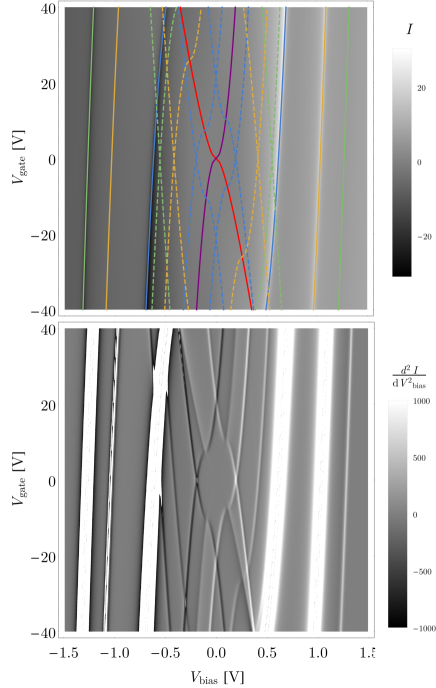
This explains the occurrence of the plateau with nearly zero current seen at low temperature in Fig. 4, and gives origin to the features in the as a function of applied bias and gate voltages as seen in the density plot of Fig. 6. At higher temperatures, all these sharp features tend to vanish, as the Fermi-Dirac occupation factors become smoother.
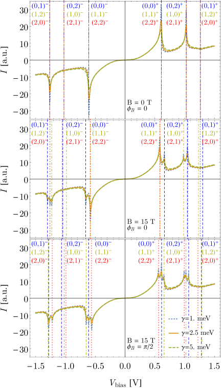
By applying an in-plane magnetic field, the threefold rotational invariance of the graphene-hBN-graphene structure is broken, and therefore, the processes corresponding to the different groups in (16) will contribute differently to the current, and one expects that each peak in the I-V curve will split into three. An in-plane magnetic field of the form can be described by the vector potential . Neglecting the momentum dependence of the effect of the in-plane magnetic field reduces to an additional transference of momentum to the tunneling electrons,, which is encoded in a shift in the vectors Brey et al. (1988); Hayden et al. (1991); Fal’ko and Meshkov (1991); Brey (2014); Mishchenko et al. (2014)
| (47) |
The splitting of the peaks in the I-V curve is shown in Fig. (7), where it is also shown the effect of an increasing electronic broadening factor.
Finally, we comment the possible effect of the hBN in the electronic structure of graphene. It is known that the potential modulation with the periodicity of the Moir pattern formed by graphene on top of hBN can lead to a reconstruction of the density of states of graphene at energies measured from the original Dirac cone, where is the wavevector of the Moir pattern reciprocal lattice Park et al. (2008); Yankowitz et al. (2012); Ortix et al. (2012); Wallbank et al. (2013); Mucha-Kruczyński et al. (2013); Ponomarenko et al. (2013) with is the rotation angle between the graphene layer and the hBN slab. We have disregarded such effects in our discussion. As we have seen in Fig. (5), the additional peaks in the current enabled by the transference of momentum by the hBN lattice, only appear for reasonable values of the bias voltage for small twist angles between the graphene layers and hBN slab. It is precisely in this case that that the reconstruction of the graphene dispersion relations becomes important at low energy. The effect of this reconstruction should impact not only the peaks that involve transference of momentum by the hBN lattice (), but also the ones that do not (). In this situation one can question the validity of the results from these section. However, we argue that the possible reconstruction of the graphene dispersion relations, should not affect in a profound way the occurrence of peaks and NDC in the I-V curves of graphene-hBN-graphene devices. The energy width, , where the reconstruction of the linear dispersion relation of graphene is significant is of the order of the tens of meVYankowitz et al. (2012); DaSilva et al. (2015), while the total energy window of states that contribute to the current is, at low temperatures, of the width of . Provided the condition is satisfied (see Fig. (8)), we expect that the effect of the dispersion relation reconstruction is negligible, and apart from a possible reduction of the height of the peaks, should not affect the current in any drastic way.
IV Incoherent current: phonon and disorder assisted tunneling
IV.1 General discussion
We will now study, in a unified way, the effect of phonons and disorder in the current of a graphene-hBN-graphene device. We consider a generic electron-phonon interaction described by the Hamiltonian
| (48) |
where is the phonon field operator, with the creation operator for a phonon mode , is an electron-phonon coupling matrix and is row vector of electronic creation operators in an arbitrary basis. For this electron-phonon interaction, the Fock (or sunset)333We point out that the Hartree (or tadpole) self-energy is local in time and as such does not give origin to lesser/greater self-energy terms, contributing only to the retarded/advanced self-energies. contribution to the lesser/greater self-energy is given by (from now on we write all frequency arguments explicitly)
| (49) |
where is the lesser/greater Green’s function for the phonon field operator, which, assuming the phonons are in thermal equilibrium, are given by
| (50) |
where is the Bose-Einstein distribution function, which satisfies , and is phonon frequency of mode . Therefore, the self-energy due to electron-phonon interaction reads
| (51) |
We point out that this self-energy can also describe elastic scattering by impurities by drop the summation over , take and set , in which case the quantity is to be interpreted as the disorder correlator. With this in mind, the following discussion applies both to inelastic scattering by phonons and elastic scattering by impurities. Combining Eq. 51 with Eqs. (25) and (26), it is possible to write to lowest order in the electron-phonon interaction
| (52) |
with obtained by replacing and . Inserting this expression in Eq. (32), we obtain the lowest order contribution to the non-coherent current
| (53) |
where the 1-phonon (disorder) assisted transmission function is given by
| (54) |
It is easy to check that
| (55) |
and as such the last two terms of Eq. (53) cancel each other. This cancellation is required since in a steady state no charge accumulation can occur in the device and therefore, the current flowing from the top to the bottom contact should satisfy . As such, terms that involve only the occupation factor of one the contacts must cancel at the end of any calculation. Processes assisted by a greater number of phonons can also be obtained. Higher order corrections to Eq. (52) can be obtained by iterating Eq. (51) using Eqs. (25) and (26). Just as for the lowest order case, contributions involving only occupation factors from one of the contacts cancel each other. Therefore, the contribution to the incoherent current assisted by phonons can be written as
| (56) |
where we have defined the -phonon assisted transmission functions
| (57) |
| (58) |
Notice that with respect to Eq. (53), we have made a change of in the first line and made a shift in the frequency variable in the second line of Eq. (56). Eqs. (56), (57) and (58) have a very simple interpretation. The first/second line of Eq. (56) can be understood has the probability of an electron being injected from the bottom/top contact being collected by the top/bottom contact, while being scattering by phonons during the contact to contact trip, with representing a phonon absorption/emission process. We will now use this general formalism to study the effect of phonon scattering in vertical transport in a graphene-hBN-graphene device. We will analyze separately the effect of scattering by graphene and hBN phonons.

IV.1.1 Scattering by phonons in the graphene layers
We know return to the issue of the consequences of considering graphene as part of the external contacts or part of the central mesoscopic region. We will first study the effect of multiple scatterings of electrons in the graphene layers by phonons (or impurities). We will first focus on scattering by phonons in the top graphene layer, with scattering in the bottom layer being treated in the same way. Using Eq. (57), the tunneling amplitude assisted by phonon scattering events in the the top graphene layer can be written to lowest order in the graphene-hBN coupling as
| (59) |
and similarly for . These contributions correspond to multiple scatterings of an electron before leaving the top graphene layer. Summing up all the contributions of the form of Eq. (59), together with the contribution from the coherent current, we obtain
| (60) |
where we have written , since we are considering only scattering in the top graphene layer. It can be checked that the different terms obey the following recursion relation
| (61) | ||||
| (62) |
This can be compared with the spectral function of the top graphene layer. Assuming that the top graphene layer is in near equilibrium with the top contact, then the spectral function can be written as
| (63) |
where, under the approximation that the top graphene is in equilibrium with the top contact, the decay rate due to electron-phonon interaction can be written as
| (64) | |||||
It is easy to check that the equilibrium occupation functions satisfy the equality
| (65) |
Therefore, by inserting Eq. (64) into Eq. (63) and iterating the equation, we obtain
| (66) |
with the different terms coincide with Eqs. (61) and (62), and the means we are making the approximation that the top graphene layer is in near equilibrium with the top contact. Therefore, the sum of all incoherent scattering processes occurring before the electron leaves the graphene layer and the coherent contribution reproduces the spectral function of graphene taking into account electron-phonon interaction / disorder. The same is true for scattering in the bottom graphene layer. Notice that in Eqs. (57) and (58) retarded/advanced Green’s functions appear to the right/left of . Nevertheless, by using Eq. (22), the previous calculation can also be applied for scattering in the bottom graphene layer. We have thus arrived to an important conclusion: the expression
| (67) | |||||
which would be the one obtained if we employed approach (A), actually already includes the effect of multiple non-coherent scattering processes in the graphene layers, provided are replaced with the respective expressions in the presence of phonon/disorder scattering. We also point out that in the case of elastic scattering due to disorder in the graphene layers, the result from Eq. (67) can be obtained by performing disorder averages of Eq. (37), see Appendix F. To lowest order in the graphene-hBN coupling, Eq. (67) actually includes all the possible scattering processes of an electron in the graphene layers. Including the effects of graphene into the Green’s function of hBN that appears in , Eq. (67) includes only a subclass of all possible contributions due to electron-phonon interaction, see Fig. 9. Therefore, we conclude that approaches (A) and (B) coincide to lowest order in the graphene-hBN coupling and to higher order in this coupling, approach (A) can correctly capture a class of all the possible electron phonon scatterings.
IV.1.2 Scattering by phonons in the hBN slab
We will now discuss the effects of scattering by phonons/disorder in the hBN slab. We will restrict ourselves to the case of tunneling assisted by one phonon. We write the electron phonon interaction in a Bloch state basis as
| (68) |
where and is the phonon field operator and is the number of unit cells in the hBN slab. For small rotation angles between the different layers and assuming only scattering by phonons close to the or points of hBN, such that only states close to the Dirac points of each layer are involved, using Eq. 56, we can write the 1-phonon assisted tunneling current to lowest order in the graphene-hBN coupling as
where we have introduced the phonon assisted tunneling amplitude between the graphene layers
Neglecting the momentum and frequency dependence of and assuming dispersionless phonons, one can make a shift in the momentum variable , such that the summation over and factors and we can write
| (69) |
, where is the area of the unit cell of hBN and graphene’s density of states per spin and valley is given by
| (70) |
where the last equality is valid for for non-interacting electrons in pristine graphene. A similar expression to Eq. (69), which included only processes involving spontaneous emission of phonons (equivalent to assuming that the phonons are at zero temperature), was recently presented without derivation and used in Ref. Vdovin et al., 2015 to model vertical current in graphene-hBN-graphene devices. In the case of elastic scattering by disorder with short range correlation, Eq. (69) becomes,
| (71) | |||||
with a disorder assisted tunneling amplitude. Although an expression of the form of Eq. 71 was previously used to model vertical current in graphene-hBN-graphene devices Britnell et al. (2012a, b), we emphasize that Eq. 71 only describes processes where there is a complete degradation of in-plane momentum conservation, something that has been previously pointed out in Refs. Brey, 2014; de la Barrera and Feenstra, 2015. The complete degradation of momentum conservation only occurs for scattering by dispersionless phonons or for disorder with short distance correlation.
As an example we consider, scattering by optical out-of-plane breathing modes close to the point, with non-zero components of polarization vector given by
| (72) |
where is the reduced mass of the hBN phonon mode. We assume that electron-phonon coupling for this mode can be described as a local change in the value of the interlayer hoping parameter in Hamiltonian 4. Considering electrons due close to the point and phonons close to the point, we derive an electron-phonon Hamiltonian of the form of Eq. 68, with a momentum independent coupling constant which reads
| (73) |
with the electron-phonon coupling constant given by
| (74) |
where describes the change of the interlayer hopping, , with the interlayer distance, , and is the out-of-plane breathing phonon frequency: For this electron-phonon interaction we obtain to lowest order in and neglecting the frequency and momentum dependence
with given by Eq. (42).
IV.2 Results
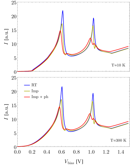
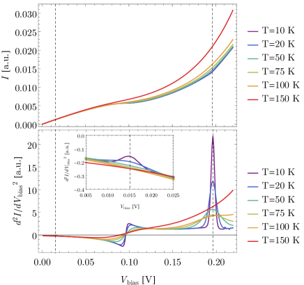
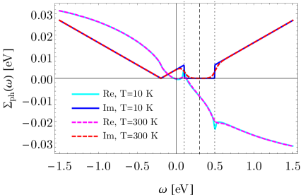
In Fig. 10 we show the vertical current as a function of bias voltage taking into account the effect of scattering of graphene electrons by resonant scatterers (treated within the SCBA, see Appendix D) and in-plane graphene electrons (see Appendix E). For comparison we also show current computed used a constant relaxation time. The main difference between modeling electron scattering with a constant relaxation rate or considering scattering by resonant scatters, is that for resonant scatters the electron decay rate has a strong dependence in energy, behaving as . Therefore, for higher bias voltages (when the graphene Fermi levels are higher), the electron lifetime is larger. This is manifest in Fig. 10, where it is seen that when assuming a constant relaxation rate the second peak in the I-V current is considerably smaller than the first one, while for resonant scatterers both peaks are roughly the same height. Inclusion of phonons, makes again the peak at higher bias voltage smaller due to the fact that the decay rate due to scattering with graphene in-plane optical phonons increases with frequency. Also notice that inclusion of resonant disorder and phonons leads to a small splitting of the peaks in the I-V current. This splitting is due to real part of the self-energy due to both resonant scatterers and phonons. Apart from increasing graphene electron’s decay rate and as such providing an additional broadening of peaks in the I-V current, phonons do not play a relevant role for the high bias I-V characteristics of a graphene-hBN-graphene device. This changes if one focus on small bias. At very low temperature, the spontaneous emission of optical phonons becomes possible whenever , where is the optical phonon frequency, opening up new tunneling channels for electrons. Although for small electron-phonon coupling, this phonon assisted contribution to the current is small the opening up of a new tunneling channel can be observed in the derivatives of the current with respect to the bias, as can be seen in Fig. 11. The features in are only significant at low temperature, being smoothed out at higher temperatures due to the smearing of the Fermi occupation factors in graphene. We point out however, that the features due to phonons are a small contribution can be overridden due to features in the coherent current induced by the rotation between different layers (shown in Fig. 6), even if we treat the phonons as dispersionless leading to a complete degradation of electron momentum conservation. We also note in passing, that tunneling assisted by emission of multiple phonons is also possible (see Eqs. (56)-(58)) which would open up new scattering channels when , where is the number of phonons. These would lead to additional peaks in but would be instead suppressed by higher powers of the electron-phonon coupling.
V Conclusions
This works provides another example of the extreme sensitivity of the properties of vdW structures to the rotational alignment of the different constitutive layers. We have seen how this additional degree of freedom can be exploited in order to create devices displaying multiple regions of negative differential conductance. The development of devices that display multiple NDC regions is relevant for the development of multivalued logic devices Sen et al. (1987, 1988), which showcases another possible application of vdW structures. We have studied in detail the effect of the rotational alignment between the boron nitride slab and the graphene layers in the vertical current of a graphene-hBN-graphene vdW structure for small rotational misalignment, which have so far not been observedMishchenko et al. (2014). We have seen now the transference of momentum by the hBN crystalline structure to the tunneling electrons gives origin to additional peaks in the I-V characteristics of this device, followed by regions of negative differential conductance. These additional peaks are however extremely sensitive to the rotation angle between the graphene layers and the hBN slab, and rotational angles as small as can already push these additional peaks to bias voltages higher than V. Therefore, the observation of multiple NDC in graphene-hBN-graphene devices requires a control of the rotational angle between the different layers with a precision of , something which is within experimental reach Ponomarenko et al. (2013); Woods et al. (2014); Mishchenko et al. (2014). We expect that the possible reconstruction of graphene spectrum due to the periodic potential induced by hBN for small rotational angles should not affect in a qualitative way the occurrence of multiple NDC regions in graphene-hBN-graphene devices, provided the applied bias voltage is much larger than the width of the region where the spectrum reconstruction is significant. However, a more quantitative treatment of these effects is required.
We have also analyzed the effect of treating graphene as being the source and drain contacts of the graphene-hBN-graphene device, or by treating them as part of the device and taking the source and drain as being external metallic contacts. We have seen that, provided the metallic contacts do not significantly spoil translation invariance of graphene (as expected if the contact is deposited only over a small region of the graphene layer), and in the non-interacting case, both approaches are equivalent. In the presence of interactions both approaches are equivalent to lowest order in the graphene-hBN coupling.
Finally, we have studied, in a unified way, the effect of scattering by disorder and phonon scattering in the vertical current of graphene-hBN-graphene devices. Starting from a NEGF formalism we derived the contribution to the current due to phonon (or disorder) assisted tunneling processes. We have seen now scattering by short range disorder or dispersionless phonons leads to a complete degradation of electron momentum conservation in the graphene-to-graphene tunneling process and how spontaneous emission of phonons at lower temperature appear as sharp features in the derivatives of the current with respect to the bias voltage at the energy of the phonons. These features can however be hidden by features due to the rotational alignment between the different layers. We have focused on the effect of graphene in-plane optical phonons and hBN optical out-of-plane breathing phonons. We have not considered the effect of vibrations at the graphene-hBN interface, as these would require the description of phonons in incommensurate structures something which will be focus of future work.
Acknowledgements.
B. Amorim acknowledges financial support from Fundação para a Ciência e a Tecnologia (Portugal), through Grant No. SFRH/BD/78987/2011. R.M. Ribeiro and N.M.R. Peres acknowledge the financial support of EC under Graphene Flagship (Contract No. CNECT-ICT-604391). N. M. R. Peres acknowledges financial support from the FCT project EXPL-FIS-NAN-1728-2013.Appendix A Thomas-Fermi modeling of electrostatic doping
We wish to model the charging of an a graphene-hBN-graphene device by application of a gate, , and bias, , voltages. The graphene-hBN-graphene structure is formed by hBN monolayers, sandwiched between two graphene layers. The graphene-hBN-graphene structure is on top of a dielectric spacer (typically hBN/SiO2) separating the structure from a back gate, typically a highly doped Si layer. We treat each layer forming the graphene-hBN-graphene structure as a 2D film with a two dimensional charge density given by , , where indexes the Si layer, and are, respectively, the bottom and top graphene layers and index the layers of hBN slab. Layers and are separated by a distance and we assume that this is filled with a dielectric with relative constant along the direction given by given by . Applying Gauss’s law around each plate, and assuming charge neutrality, , we obtain
| (75) | |||||
| (76) | |||||
| (77) |
where is the electric field along the direction, between layers and , and is vacuum’s permittivity. From these equations we can write
| (78) |
and the stored electrostatic energy is given by
| (79) | |||||
where we have used the charge neutrality condition in order to eliminate the charge in the Si gate . This is nothing more than the Hartree energy for a layered material. We split the charge density of each layer into a contribution from charge carriers and another from charged impurities, , where is the charge carrier concentration ( for electron doping) and is the concentration of charged impurities ( for positively charged impurities). Including the effects of a gate voltage, , applied between the and the layers and a bias voltage between the and the layers, we obtain a Thomas-Fermi functional
| (80) | |||||
where
| (81) |
is the potential created by the charged impurities. The Hartree potential felt by electrons in layer is then given by
| (82) | |||||
Now, we assume that the vertical current flowing between the two graphene layers is small enough, such that we can assume that these are in a near equilibrium state. Furthermore, we employ the Thomas-Fermi approximation, in which the local Fermi level for each layer is given by , where is a function of the local carrier density. This together with Eq. (82) becomes a system of non-linear equations in the carrier density / local Fermi level.
It can be checked, that due to the large band gap of hBN, most charge density will be accumulated in the graphene layers. As such we approximate for and therefore the equations are reduced to two
| (83) | |||||
| (84) |
where the capacitances are given by (taking into account the series capacitances of a hBN/SiO2 spacer with the hBN thickness and the SiO2 thickness)
| (85) | ||||
| (86) |
and is the distance between the two graphene layers. The terms are the potentials induced by the charged impurities in the bottom/top graphene layer that can be tuned to account for intrinsic doping of the graphene layers (acting as an offset in the measurement of and ). We finally point out that in the case where the hBN layers have no charge carrier, then the Hartree potential within the hBN slab is given from Eq. (82) in terms of as
| (87) |
which in the absence of impurities reduces to the expression given in Sec. II.1. The solutions of Eqs. (83)-(84) for a particular device are shown in Fig. 12
Appendix B Interlayer hopping Hamiltonian between non-commensurate layers
We describe the graphene-boron nitride coupling using the general theory of coupling between non-commensurate layers of Refs. Bistritzer and MacDonald, 2010; Koshino, 2015. We wish to describe the coupling between two 2D crystals, labeled as and , with Bravais lattices spanned by and , respectively. In a tight-binding representation the interlayer hopping between layers and can be written as
| (88) |
where the indices run over Bravais lattice sites, run over orbitals/sublattice sites, creates an electron state in layer at position and orbital/sublattice , with a sublattice vector, and are hopping terms. Assuming that the hopping only depends on it is possible to write it in Fourier components asKoshino (2015)
where is the area of the unit cell of layer . If we express, and in a Bloch basis
| (89) | |||||
| (90) |
where is the number of unit cells in layer , such that, the interlayer Hamiltonian becomes
| (91) |
where are reciprocal lattice vectors of the 2D crystal . The Kronecker- imposes that in a interlayer hoping process, momentum is conserved modulo any combination of reciprocal lattice vectors of both layers. In general, will decay for large values of , and therefore only the processes with smallest need be considered.
We now specialize to the case where is a graphene layer and is a boron nitride layer. The graphene unit cell contains two carbon atoms in the unit cell, A and B, while boron nitride contains one boron atom, B, and one nitrogen atom, N, in the unit cell, see Fig. 1. We will focus on low energy states, which lie close to the Dirac points, , of the graphene layer. Considering only the three most relevant processes coupling the graphene and boron nitride layers, we must consider processes involving and for states close to the point and processes involving and for states close to the point. It is also assumed that the momentum dependence of is weak such that we can approximate , setting : and .
In order to describe the coupling between the bottom and top graphene layers to a slab formed by hBN monolayers, we notice that the products of unit cell basis vectors and reciprocal lattice vectors that appears in Eq. (91) can be written for the bottom graphene layer as and (for states close to point). For the coupling between the top graphene layer and the hBN layer, one must consider separately the cases when the hBN slab is formed by and even or odd number of layers. For an odd number of layers, in the th layer the boron and nitrogen atoms occupy the same positions as in the 1st layer and therefore we still have and . If we have an even number of hBN layers, then in the layer, the boron an nitrogen atoms switch positions compared to the 1st layer, and one obtains instead and . With these approximations, one obtains Eq. (5) of the main text.
Appendix C Analytic expression for the tunneling density of states
In this appendix we provide an analytic expression for Eq. (44). First, we notice that Eq. (44) can be written in a the graphene sublattice basis as
| (92) |
where is the trace over graphene sublattice indices, is a matrix of ones, and we have written the spectral function in the sublattice basis as
| (93) |
where the graphene retarded/advanced electron Green´s function in the sublattice space is given by
| (94) |
with . In the limit of an infinite electron lifetime, we have . In the presence of perturbations that induce a momentum independent self-energy that is diagonal in the sublattice basis (such as short range diagonal disorder or scattering by in-plane optical phonons), we make the replacement , where is the broadening factor. In the presence of the external metallic contacts and disorder/phonon scattering, we obtain . In terms of Green’s functions, and noticing that the matrices perform a rotation of the electronic Green’s functions, can be written as
| (95) |
Performing the trace over the sublattice degrees of freedom we get
| (96) |
The advantage of this form, with respect to Eq. (44), is that Eq. (96) is analytic in and as such, contour integration methods can be used to compute the integrals. In order to make analytic progress, in the first term of the previous expression we take the limit , such that and
| (97) |
We use the -function to perform the integration over , obtaining
| (98) |
The remaining integration over the angular variable can be performed using contour integration methods. Performing a change of variables such that
| (99) | |||||
| (100) |
Eq. (98) can be written as an integral over the variable around the unit circle in the complex plane
| (101) |
with the angle of the vector with the reference axis. The integrand has a double pole at and two simple poles at , with
| (102) | ||||
| (103) | ||||
| (104) |
defined such that and . The contour integration around the unit circle can be performed analytically collecting the residues at and . Notice that we have made the approximation . In general, both and will be non-zero. The simplest way to that this into account is to symmetrize Eq. (96) with respect to the bottom and the top graphene layer an then taking the limit in the first term and in the second. The final symmetrized result is given by
| (105) |
where we have introduced the quantities
| (106) |
and the quantities and given by Eqs. (103) and (104) with the replacements and It was checked that Eq. (105) provides a very good approximation to the numeric evaluation of Eq. (96) when both and are non-zero, if the broadening function for each layer is assumed to the the sum of the broadening factors of both layers, i.e., performing the replacement .
In the limit of infinite electron lifetime in both layers , we obtain
| (107) | |||||
| (108) |
and are obtained by replacing . and simplifies to
| (109) |
We notice that, in this limit, is only non-zero when .
We finally study how the spinorial character of graphene’s wavefunction manifests in the form of . If we set the wavefunction overlap factors to in Eq. (44), then instead of Eq. (96) we would obtain
| (110) |
In order to evaluate , we proceed as previously. the only difference is that when performing the integration over the unit circle in the complex variable , there is no double pole at , and the contour integration only collects the contribution from . Symmetrizing the result, this leads to
| (111) |
Appendix D Resonant impurities within the SCBA
We consider the effect of resonant impurities, such as vacancies, in the properties of graphene. We focus on this kind of impurities due to the possibility for analytical progress and due to the fact that this model for impurities correctly predicts a transport lifetime in graphene that depends on the Fermi energy as Peres (2010). Resonances due to short range disorder cannot be taken into account by treating then within a Gaussian approximation. A way to overcome this limitation is to employ the T-matrix, which properly takes into account multiple scatterings by the same impurity in the limit of low impurity concentration. Using the T-matrix within the non-crossing approximation, the self-consistent Born approximation (SCBA) for the Green’s function of an isolated graphene layer reads
| (112) |
where matrices the have indices in the sublattice space, a bar denotes disorder averaging and is the impurity self-energy, where is the impurity concentration (number of impurities by graphene unit cell) and is the T-matrix for a single -like impurity with strength . For an impurity potential diagonal in the sublattice basis, the T-matrix is also diagonal with equal components, given by
| (113) |
where we have taken the limit in order to describe vacancies and defined
| (114) |
In the Dirac cone approximation, graphene Green’s function in the sublattice basis and taking into account a finite electron life (induce by the metallic contact) is given by
| (115) |
with , indices running over the A, B sublattice sites and is the lifetime induced by the metallic contacts, (assuming the metallic contacts couple equally to all graphene states and do not spoil translational invariance of graphene). For resonant impurities, the self-energy is momentum independent. Writing it as , we can evaluate analytically obtaining
| (116) | |||||
where the functions and are given by
| (117) | ||||
| (118) |
with a high energy cutoff. In terms of and the self-energy is given by
| (119) | |||||
| (120) |
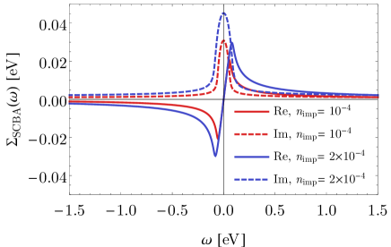
where we have defined , and is a constant characterizing the scattering by resonant disorder. Eqs. (117)-(120) form a set of equations that can be easily solved. The solution for self-energy is shown in Fig. 13.
Appendix E Graphene electron self-energy due to in-plane optical phonons
Electron-phonon interaction in graphene can be modeled by starting from a nearest neighbour tight-binding Hamiltonian for the electrons and assuming that the lattice distortions due to phonons lead to a modulation of hopping integralsSuzuura and Ando (2002). For graphene longitudinal and transverse in-plane phonons close to the point and electrons close to the point the obtained electron-phonon interaction Hamiltonian is given by
| (121) |
wheres
| (122) |
is the electron-phonon coupling constant, with describing the change in the nearest neighbour hopping, , with the distance, ; is the reduced mass of the phonon mode, with the carbon atom mass; and is the phonon dispersion for the longitudinal/transverse in-plane optical phonon mode (which are degenerate at and and assume we approximate them as dispersionless). The polarization vectors for the longitudinal and transverse mode can be written as and . With these approximations we obtain the momentum independent electron-phonon interaction matrices
| (123) | |||||
| (124) |
Assuming the graphene layer is in thermal equilibrium and to lowest order in the electron-phonon interaction, the self energy is diagonal in sublattice space and given by
| (125) |
The imaginary part can be computed for pristine graphene at finite temperature as
| (126) |
where and the Fermi energy, , are both measured from the Dirac cone. From this, the real part can be efficiently obtained using the Kramers-Kronig relation
| (127) |
The computed self-energy is shown in Fig. 14.
Appendix F Vertex corrections for resonant impurities
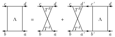
In this Appendix, we provide an alternative derivation of Eq. (67), for the vertical current in a graphene-hBN-graphene device taking into account disorder in the graphene layers, employing approach (B). Instead of describing disorder as an interaction, we will start from Eq. (37) and perform disorder averages of it. Just as in Appendix. D we will consider scattering by resonant disorder. This model will both serve as a concrete example for elastic scattering of the general results present in Sec. IV regarding the equivalences of approaches (A) and (B) and will also show the formal equivalence between the contributions to the current arising from Eq. (32) and vertex corrections. Just as in Sec. III we will assume for simplicity that the external metallic contacts couple to all graphene states and that graphene electronic states are still well describe by Bloch states. With these approximations, we write
| (128) |
Performing an averaging of Eq. (37) with respect to disorder in the bottom and top graphene layers, assuming that these are uncorrelated, and to lowest order in the graphene-hBN coupling we obtain
| (130) | |||||
The disorder averaged product of Green’s functions is not just the product of average Green’s function, as the averaging procedure establishes correlations between the two functions. From now on, we will employing a notation where an upper indice represents an out-going electronic state and a lower indice represents an incoming state, with repeated indices being summed over. With this convention, the average of the product of two Green’s functions, in sublattice space, can be written as (suppressing the frequency argument and the bg/tg indice)
| (131) |
where the second term are vertex corrections, we have define the quantity
| (132) |
and is a 4-point function, which obeys a Bethe-Salpeter equation (see Fig. 15)
| (133) |
where is an irreducible 4-point function, which within the T-matrix and non-crossing approximation for resonant impurities is given by
| (134) |
The quantity can be evaluated analytically yielding
| (135) |
where
| (136) | |||||
| (137) |
with the functions and defined by Eqs. (117), (118) and where we have written and as in Appendix. D. The Bethe-Salpeter equation for is now a simple problem of linear algebra. Solving Eq. (133), yields the non-zero components of in the sublattice basis
| (138) | |||||
| (139) | |||||
| (140) |
, where we have omitted the frequency arguments of . Using the fact that , the vertex correction contribution in Eq. (131) can be written as
| (141) |
Expressing and in terms of and , and using Eqs. (120) it can be seen that the quantity can be written as the ratio
| (142) |
Therefore, Eq. (131) can be written as
| (143) |
Therefore, the product of a retarded and an advanced Green function is related to the spectral function as
| (144) |
and therefore, the contributions from vertex corrections (incoherent contributions) due to impurities adds to the contribution coming from the product of two average Green’s functions (coherent contribution), in such a way that Eq. (130) reduces to Eq. (38) of the main text. This result is a particular case of the more general discussion of Sec. IV.1.1, which is not limited to elastic scattering.
References
- Novoselov et al. (2004) K. S. Novoselov, A. K. Geim, S. V. Morozov, D. Jiang, Y. Zhang, S. V. Dubonos, I. V. Grigorieva, and A. A. Firsov, Science 306, 666 (2004), http://www.sciencemag.org/content/306/5696/666.full.pdf .
- Novoselov et al. (2005) K. S. Novoselov, D. Jiang, F. Schedin, T. J. Booth, V. V. Khotkevich, S. V. Morozov, and A. K. Geim, Proceedings of the National Academy of Sciences of the United States of America 102, 10451 (2005), http://www.pnas.org/content/102/30/10451.full.pdf .
- Ponomarenko L. A. et al. (2011) Ponomarenko L. A., Geim A. K., Zhukov A. A., Jalil R., Morozov S. V., Novoselov K. S., Grigorieva I. V., Hill E. H., Cheianov V. V., Fal/’ko V. I., Watanabe K., Taniguchi T., and Gorbachev R. V., Nat Phys 7, 958 (2011), 10.1038/nphys2114.
- Novoselov and Neto (2012) K. S. Novoselov and A. H. C. Neto, Physica Scripta 2012, 014006 (2012).
- (5) Geim A. K. and Grigorieva I. V., 10.1038/nature12385 10.1038/nature12385.
- Britnell et al. (2012a) L. Britnell, R. V. Gorbachev, R. Jalil, B. D. Belle, F. Schedin, A. Mishchenko, T. Georgiou, M. I. Katsnelson, L. Eaves, S. V. Morozov, N. M. R. Peres, J. Leist, A. K. Geim, K. S. Novoselov, and L. A. Ponomarenko, Science 335, 947 (2012a), http://www.sciencemag.org/content/335/6071/947.full.pdf .
- Britnell et al. (2012b) L. Britnell, R. V. Gorbachev, R. Jalil, B. D. Belle, F. Schedin, M. I. Katsnelson, L. Eaves, S. V. Morozov, A. S. Mayorov, N. M. R. Peres, A. H. C. Neto, J. Leist, A. K. Geim, L. A. Ponomarenko, and K. S. Novoselov, Nano Letters 12, 1707 (2012b), pMID: 22380756, http://dx.doi.org/10.1021/nl3002205 .
- Georgiou Thanasis et al. (2013) Georgiou Thanasis, Jalil Rashid, Belle Branson D., Britnell Liam, Gorbachev Roman V., Morozov Sergey V., Kim Yong-Jin, Gholinia Ali, Haigh Sarah J., Makarovsky Oleg, Eaves Laurence, Ponomarenko Leonid A., Geim Andre K., Novoselov Kostya S., and Mishchenko Artem, Nat Nano 8, 100 (2013).
- Britnell et al. (2013) L. Britnell, R. M. Ribeiro, A. Eckmann, R. Jalil, B. D. Belle, A. Mishchenko, Y.-J. Kim, R. V. Gorbachev, T. Georgiou, S. V. Morozov, A. N. Grigorenko, A. K. Geim, C. Casiraghi, A. H. C. Neto, and K. S. Novoselov, Science 340, 1311 (2013), http://www.sciencemag.org/content/340/6138/1311.full.pdf .
- Yu Woo Jong et al. (2013) Yu Woo Jong, Liu Yuan, Zhou Hailong, Yin Anxiang, Li Zheng, Huang Yu, and Duan Xiangfeng, Nat Nano 8, 952 (2013).
- Massicotte et al. (2016) M. Massicotte, P. Schmidt, F. Vialla, K. G. Schädler, A. Reserbat-Plantey, K. Watanabe, T. Taniguchi, K.-J. Tielrooij, and F. H. L. Koppens, Nat Nano 11, 42 (2016).
- Haigh et al. (2012) S. J. Haigh, A. Gholinia, R. Jalil, S. Romani, L. Britnell, D. C. Elias, K. S. Novoselov, L. A. Ponomarenko, A. K. Geim, and R. Gorbachev, Nat Mater 11, 764 (2012).
- Pong and Durkan (2005) W.-T. Pong and C. Durkan, Journal of Physics D: Applied Physics 38, R329 (2005).
- Lopes dos Santos et al. (2007) J. M. B. Lopes dos Santos, N. M. R. Peres, and A. H. Castro Neto, Phys. Rev. Lett. 99, 256802 (2007).
- Luican et al. (2011) A. Luican, G. Li, A. Reina, J. Kong, R. R. Nair, K. S. Novoselov, A. K. Geim, and E. Y. Andrei, Phys. Rev. Lett. 106, 126802 (2011).
- Park et al. (2008) C.-H. Park, L. Yang, Y.-W. Son, M. L. Cohen, and S. G. Louie, Phys. Rev. Lett. 101, 126804 (2008).
- Yankowitz et al. (2012) M. Yankowitz, J. Xue, D. Cormode, J. D. Sanchez-Yamagishi, K. Watanabe, T. Taniguchi, P. Jarillo-Herrero, P. Jacquod, and B. J. LeRoy, Nat Phys 8, 382 (2012).
- Ortix et al. (2012) C. Ortix, L. Yang, and J. van den Brink, Phys. Rev. B 86, 081405 (2012).
- Wallbank et al. (2013) J. R. Wallbank, A. A. Patel, M. Mucha-Kruczyński, A. K. Geim, and V. I. Fal’ko, Phys. Rev. B 87, 245408 (2013).
- Mucha-Kruczyński et al. (2013) M. Mucha-Kruczyński, J. R. Wallbank, and V. I. Fal’ko, Phys. Rev. B 88, 205418 (2013).
- Ponomarenko et al. (2013) L. A. Ponomarenko, R. V. Gorbachev, G. L. Yu, D. C. Elias, R. Jalil, A. A. Patel, A. Mishchenko, A. S. Mayorov, C. R. Woods, J. R. Wallbank, M. Mucha-Kruczynski, B. A. Piot, M. Potemski, I. V. Grigorieva, K. S. Novoselov, F. Guinea, V. I. Fal/’ko, and A. K. Geim, Nature 497, 594 (2013).
- Bistritzer and MacDonald (2010) R. Bistritzer and A. H. MacDonald, Phys. Rev. B 81, 245412 (2010).
- Mishchenko et al. (2014) A. Mishchenko, J. Tu, Y. Cao, R. V. Gorbachev, J. R. Wallbank, M. T. Greenaway, V. E. Morozov, S. V. Morozov, M. J. Zhu, S. L. Wong, F. Withers, C. R. Woods, Y.-J. Kim, K. Watanabe, T. Taniguchi, E. E. Vdovin, O. Makarovsky, T. M. Fromhold, V. I. Fal’ko, G. A. K., L. Eaves, and K. S. Novoselov, Nat Nano 9, 808 (2014).
- Brey (2014) L. Brey, Phys. Rev. Applied 2, 014003 (2014).
- Fallahazad et al. (2015) B. Fallahazad, K. Lee, S. Kang, J. Xue, S. Larentis, C. Corbet, K. Kim, H. C. P. Movva, T. Taniguchi, K. Watanabe, L. F. Register, S. K. Banerjee, and E. Tutuc, Nano Letters 15, 428 (2015), pMID: 25436861, http://dx.doi.org/10.1021/nl503756y .
- Kang et al. (2015) S. Kang, B. Fallahazad, K. Lee, H. Movva, K. Kim, C. Corbet, T. Taniguchi, K. Watanabe, L. Colombo, L. Register, E. Tutuc, and S. Banerjee, Electron Device Letters, IEEE 36, 405 (2015).
- de la Barrera and Feenstra (2015) S. C. de la Barrera and R. M. Feenstra, Applied Physics Letters 106, 093115 (2015), http://dx.doi.org/10.1063/1.4914324.
- Lane et al. (2015) T. L. M. Lane, J. R. Wallbank, and V. I. Fal’ko, Applied Physics Letters 107, 203506 (2015), http://dx.doi.org/10.1063/1.4935988.
- Perebeinos et al. (2012) V. Perebeinos, J. Tersoff, and P. Avouris, Phys. Rev. Lett. 109, 236604 (2012).
- Jung et al. (2015) S. Jung, M. Park, J. Park, T.-Y. Jeong, K. Kim, Ho-Jong Watanabe, T. Taniguchi, D. H. Ha, C. Hwang, and Y.-S. Kim, Scientific Reports 5 (2015), 10.1038/srep16642.
- Vdovin et al. (2015) E. E. Vdovin, A. Mishchenko, M. T. Greenaway, M. J. Zhu, D. Ghazaryan, A. Misra, Y. Cao, S. V. Morozov, O. Makarovsky, A. Patanè, G. J. Slotman, M. I. Katsnelson, A. K. Geim, K. S. Novoselov, and L. Eaves, ArXiv e-prints (2015), arXiv:1512.02143 [cond-mat.mes-hall] .
- Peres (2010) N. M. R. Peres, Rev. Mod. Phys. 82, 2673 (2010).
- Geick et al. (1966) R. Geick, C. H. Perry, and G. Rupprecht, Phys. Rev. 146, 543 (1966).
- Ribeiro and Peres (2011) R. M. Ribeiro and N. M. R. Peres, Phys. Rev. B 83, 235312 (2011).
- Kindermann et al. (2012) M. Kindermann, B. Uchoa, and D. L. Miller, Phys. Rev. B 86, 115415 (2012).
- Jung et al. (2014) J. Jung, A. Raoux, Z. Qiao, and A. H. MacDonald, Phys. Rev. B 89, 205414 (2014).
- Koshino (2015) M. Koshino, New Journal of Physics 17, 015014 (2015).
- Bistritzer and MacDonald (2011) R. Bistritzer and A. H. MacDonald, Proceedings of the National Academy of Sciences of the United States of America 108, 12233 (2011).
- Lopes dos Santos et al. (2012) J. M. B. Lopes dos Santos, N. M. R. Peres, and A. H. Castro Neto, Phys. Rev. B 86, 155449 (2012).
- Moon and Koshino (2013) P. Moon and M. Koshino, Phys. Rev. B 87, 205404 (2013).
- Moon and Koshino (2014) P. Moon and M. Koshino, Phys. Rev. B 90, 155406 (2014).
- Note (1) In Ref. Brey, 2014, the processes corresponding to and where identified as being equivalent, with . This was likely caused by first expanding to linear order in , and , and only then evaluating , loosing in the process terms involving the product in , which lift the equivalence between the processes associated with and .
- Frensley (1990) W. R. Frensley, Rev. Mod. Phys. 62, 745 (1990).
- Vogl and Kubis (2010) P. Vogl and T. Kubis, Journal of Computational Electronics 9, 237 (2010).
- Stone and Szafer (1988) S. D. Stone and A. Szafer, IBM J. Res. Dev. 32, 384 (1988).
- Note (2) In mesoscopic transport, the problem of computing the current that is flowing through the device is reduced to a problem only involving degrees of freedom in the mesoscopic region by integrating out the external contacts. This is only done exactly provided the contacts are non-interacting.
- Haug and Jauho (2008) H. Haug and A.-P. Jauho, Quantum Kinetics in Transport and Optics of Semiconductors, 2nd ed., Springer Series in Solid-State Sciences, Vol. 123 (Springer-Verlag Berlin, Heidelberg, 2008).
- Datta (1997) S. Datta, Electronic Transport in Mesoscopic Systems, Cambridge Studies in Semiconductor Physics and Microelectronic Engineering (Cambridge University Press, 1997).
- Feenstra et al. (2012) R. M. Feenstra, D. Jena, and G. Gu, Journal of Applied Physics 111, 043711 (2012), http://dx.doi.org/10.1063/1.3686639.
- Vasko (2013) F. T. Vasko, Phys. Rev. B 87, 075424 (2013).
- Brey et al. (1988) L. Brey, G. Platero, and C. Tejedor, Phys. Rev. B 38, 9649 (1988).
- Hayden et al. (1991) R. K. Hayden, D. K. Maude, L. Eaves, E. C. Valadares, M. Henini, F. W. Sheard, O. H. Hughes, J. C. Portal, and L. Cury, Phys. Rev. Lett. 66, 1749 (1991).
- Fal’ko and Meshkov (1991) V. I. Fal’ko and S. V. Meshkov, Semiconductor Science and Technology 6, 196 (1991).
- DaSilva et al. (2015) A. M. DaSilva, J. Jung, S. Adam, and A. H. MacDonald, Phys. Rev. B 92, 155406 (2015).
- Note (3) We point out that the Hartree (or tadpole) self-energy is local in time and as such does not give origin to lesser/greater self-energy terms, contributing only to the retarded/advanced self-energies.
- Michel and Verberck (2011) K. H. Michel and B. Verberck, Phys. Rev. B 83, 115328 (2011).
- Wirtz and Rubio (2004) L. Wirtz and A. Rubio, Solid State Communications 131, 141 (2004).
- Sen et al. (1987) S. Sen, F. Capasso, A. Y. Cho, and D. Sivco, IEEE Transactions on Electron Devices 34, 2185 (1987).
- Sen et al. (1988) S. Sen, F. Capasso, A. Y. Cho, and D. L. Sivco, IEEE Electron Device Letters 9, 533 (1988).
- Woods et al. (2014) C. R. Woods, L. Britnell, A. Eckmann, R. S. Ma, J. C. Lu, H. M. Guo, X. Lin, G. L. Yu, Y. Cao, R. V. Gorbachev, A. V. Kretinin, J. Park, L. A. Ponomarenko, M. I. Katsnelson, Y. N. Gornostyrev, K. Watanabe, T. Taniguchi, C. Casiraghi, H.-J. Gao, A. K. Geim, and K. S. Novoselov, Nat Phys 10, 451 (2014).
- Suzuura and Ando (2002) H. Suzuura and T. Ando, Phys. Rev. B 65, 235412 (2002).