Conductance Quantization at zero magnetic field in InSb nanowires
Abstract
Ballistic electron transport is a key requirement for existence of a topological phase transition in proximitized InSb nanowires. However, measurements of quantized conductance as direct evidence of ballistic transport have so far been obscured due to the increased chance of backscattering in one dimensional nanowires. We show that by improving the nanowire-metal interface as well as the dielectric environment we can consistently achieve conductance quantization at zero magnetic field. Additionally, studying the sub-band evolution in a rotating magnetic field reveals an orbital degeneracy between the second and third sub-bands for perpendicular fields above .
keywords:
Quantum point contact, conductance quantization, nanowire, InSb, subband, orbital effects]
QuTech and Kavli Institute of Nanoscience, Delft University of Technology, 2628 CJ Delft, The Netherlands
]
Advanced Materials Laboratory, National Institute for Materials Science, 1-1 Namiki, Tsukuba, 305-0044, Japan
]
Department of Applied Physics, Eindhoven University of Technology, 5600 MB Eindhoven, The Netherlands
\alsoaffiliationDepartment of Applied Physics, Eindhoven University of Technology, 5600 MB Eindhoven, The Netherlands
\alsoaffiliation[Current address: CNRS-Laboratoire d’Analyse et d’Architecture des Systemes (LAAS), Université de Toulouse, 7 avenue du Colonel Roche, F-31400 Toulouse, France]
CNRS-Laboratoire d’Analyse et d’Architecture des Systemes (LAAS), Université de Toulouse, 7 avenue du Colonel Roche, F-31400 Toulouse, France
\alsoaffiliationDepartment of Applied Physics, Eindhoven University of Technology, 5600 MB Eindhoven, The Netherlands
{tocentry}
![[Uncaptioned image]](/html/1603.03751/assets/x1.png)
Semiconducting nanowires made from InAs and InSb are prime candidates for the investigation of novel phenomena in electronic devices. The intrinsic strong spin-orbit interaction (SOI) and large g-factor combined with flexible fabrication has resulted in these materials being investigated for applications in quantum computing,1,2,3 spintronics4,5,6 and Cooper pair splitters.7,8 More recently, these nanowires have been investigated as solid-state hosts for Majorana zero modes (MZMs). 9,10,11,12 By bringing a one dimensional (1D) nanowire with strong SOI into close contact with a superconductor under an external magnetic field, a region with inverted band structure emerges, creating MZMs at its ends. Together with strong SOI and induced superconductivity, a key requirement for MZMs is quasi-ballistic electron transport along the length of the proximitized region in the nanowire, with a controlled odd number of occupied modes.13 In the absence of scattering, the motion of 1D confined electrons will be restricted to discrete energy bands resulting in quantized conductance plateaus.14,15 Measurements of quantized conductance in the nanowires therefore provide direct evidence for controlled mode occupation, as well as ballistic transport in these nanowires.
Although now routine in gate defined quantum point contacts (QPC) in two-dimensional electron gases (2DEG), 14,15,16,17,18 quantized conductance in one dimensional semiconductor nanowires is more difficult to achieve. In a 1D nanowire, scattering events along the electrons path to and through the constriction between the source and drain contacts have an increased probability of reflection, obscuring the observation of quantized conductance.19 These scattering events may be due to impurities and imperfections in the crystal lattice, or due to surface states that create inhomogeneities in the local electrostatic environment.20 A Schottky barrier between the nanowire and metallic contacts will result in additional backscattering events, further smearing out the quantized conductance plateaus. To date, quantized conductance in InSb nanowires has only been observed at high magnetic fields (), where electron backscattering is strongly suppressed.19 No quantization has been observed in InSb for magnetic fields below , where the topological transition is expected to take place.9
Here we demonstrate conductance quantization in InSb nanowires at zero magnetic field. We have developed a robust fabrication recipe for observing quantized conductance by optimizing both the metal-nanowire contact interface and dielectric environment through the use of hexagonal boron nitride (hBN) as a gate dielectric. We study the evolution of the quantized conductance plateaus with both source-drain bias as well as magnetic field, and extract values for the Landé g-factor of the first three sub-bands in the nanowire. Additionally, we observe an orbital energy degeneracy of the second and third sub-bands at finite magnetic fields applied perpendicular to the nanowire.
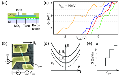
Figure 1a) shows a cross-sectional view of our devices. They consist of an intrinsic Si-substrate with local metallic gates made of Ti/Au (/), on top of which a sheet of hexagonal boron nitride (hBN) is mechanically transferred as the dielectric. The chemical stability, atomic flatness, and high breakdown voltage21, together with the well established dry transfer mechanism 22 makes hBN an ideal dielectric for our nanowire devices. InSb nanowires grown by metal-organic vapor phase epitaxy 23,24 ( - long and - diameter) are transferred deterministically with a micro-manipulator25 onto the hBN dielectric. Electrical contacts to the nanowire (evaporated Cr/Au (), - nm spacing) are defined by electron beam lithography. Before contact deposition, the surface oxide of the nanowires is removed using sulfur passivation26 followed by a short in situ He-ion mill. Residual sulfur from the passivation step also induces surface doping, which aids contact transparency. Further details of the fabrication are included in the supporting information. A top view scanning electron microscope image of a finished device is shown in Fig 1b). The samples are mounted in a dilution refrigerator with a base temperature of and measured using standard lock-in techniques at Hz with an excitation V. Voltage is applied to the outer contact and current measured through the grounded central contact, while the third, unused contact is left floating.
We first characterize each device by sweeping the voltage on the underlying gate at fixed bias voltage across the sample. Conductance is obtained directly from the measured current and an appropriate series resistance is subtracted in each case (see supporting information). Figure 1c) plots the conductance of the nanowire as function of gate voltage for four different devices fabricated on the same chip. Devices with both fine gates as well as wide back gates have been measured. We find that while fine gates allow more flexible gating, devices with wide back gates showed more pronounced conductance plateaus even after extensive tuning of the fine gates. Data from additional devices all fabricated on the same chip is included in the supporting information.
As seen in Fig 1c) all devices show well defined plateaus at and but the plateaus at and appear smaller or even completely absent. Unlike QPC’s formed in 2DEGs, nanowires possess rotational symmetry. This symmetry can give rise to additional orbital degeneracies in the energies for the 2nd and 3rd as well as the 4th and 5th sub-band (Fig 1d).27,28 In conductance measurements at finite bias, sub-bands that are close in energy or degenerate will be populated at similar values in gate voltage giving a double step of instead of , which explains the suppressed plateaus at and (Fig 1e).29
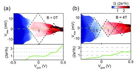
To investigate this phenomenon in more detail, we measure the differential conductance as function of gate voltage and bias voltage for one of these devices (corresponding to the green trace in Fig 1c). This data is shown in Fig 2a) as a color plot, with a line cut along zero bias voltage added in the bottom panel. At zero bias voltage an extended plateau is visible at , together with an additional small plateau at which was not visible in the linear conductance data of Figure 1c). The existence of this small plateau indicates that the device has a small, but finite energy splitting between the second and third sub-band which was not resolved at high bias. At finite bias voltage the conductance will only be quantized in integer values of if both and occupy the same sub-band. This creates diamond shaped regions of constant conductance indicated by black dotted lines in Fig 2a). At the tip of the diamond the two dotted lines cross when is equal to the sub-band energy spacing . From this we extract and the lever-arm of the bottom gate via .30, A finite magnetic field breaks time reversal symmetry, lifting spin degeneracy and splitting the individual spin sub-bands by the Zeeman energy . Here denotes the Bohr magneton and g the Landé g-factor. Experimentally this splitting manifests as the appearance of additional half integer steps . At we clearly observe this for the first sub-band as shown in Fig 2b) where an additional plateau emerges at . Similarly, the second sub-band should also split into two plateaus at and . However only the plateau is visible, suggesting that the orbital degeneracy between and remains at finite magnetic field.
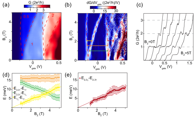
The full evolution in magnetic field of the conductance and transconductance is shown in Fig 3a,b) and individual line traces of the conductance taken in steps of are presented in Fig 3c). While the plateau at remains very flat up to high magnetic fields, the second plateau at increases in height for magnetic fields larger than . Around two new plateaus emerge with similar slope at and . These correspond to the lower energy spin sub-bands and . Here we can clearly see experimentally that the non-degenerate orbital state at zero field transforms into a degenerate orbital state at finite field and that remain degenerate over a magnetic field range of several Tesla.
From the individual gate traces we convert the plateau width to energy by using the lever arm extracted from Figure 2. This way we can directly extract the sub-band spacing and the individual g-factors , through a linear fit fixed at the origin to and . We find and a constant sub-band spacing .
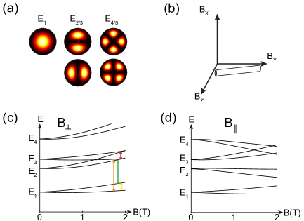
Orbital degeneracy of sub-bands has previously been observed in metallic point contacts29 and recently also in passivated narrow InAs nanowires with highly symmetric conducting channels27. However, the magnetoconductance of InSb nanowires may deviate significantly from the results found in InAs nanowires. In InAs, Fermi level pinning leads to conduction close to the nanowire surface 31,32 which strongly influences the sub-band dispersion in magnetic field.33,34 InSb has no surface accumulation35 and the electron wave-function will be more strongly confined in the center of the nanowire. For cylindrical nanowires individual sub-band wave functions are given by Bessel functions with different orbital angular momentum along the wire (Fig 4a), and numerical simulations of wires with a hexagonal cross-section show qualitatively similar results.28,36 An additional magnetic field will add Zeeman splitting, but also causes orbital effects which can substantially change the sub-band dispersion depending on the orientation of the field with respect to the nanowires axis.37 Numerical simulations of nanowires in a magnetic field show that orbital effects strongly depend on the magnetic field orientation and can dominate the sub-band dispersion, leading to a decrease of the energy splitting between and . 37 Furthermore these simulations also show that the orbital effects can strongly influence the phase diagram of MZMs. 37 Using the model of ref. 37 with the parameters of our device (wire radius: ; g-factor: ) we simulate this change in the sub-band dispersion for a magnetic field perpendicular (Fig 4c) and parallel (Fig 4d) to the nanowire. A perpendicular magnetic field causes and to shift higher and closer in energy, while a parallel magnetic field increases the energy splitting of the higher sub-bands and , due to their different orbital angular momentum.
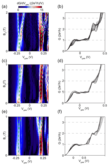
Experimentally we test this by rotating the direction of the magnetic field, as shown in Fig 5. When aligning the magnetic field along (almost perpendicular to the nanowire, Fig 5a,b), a small splitting appears at the beginning of the first plateau for fields above , marking the onset of the -plateau. In contrast, in the second plateau the splitting only starts above and the line-cuts (Fig 5b) show that the new plateau emerges at . Similarly, for a magnetic field along (Fig 5c,d), a new plateau emerges around in the first step but not in the second. However, for the magnetic field aligned along (mostly parallel to the nanowire) shown in Fig 5e,f) we do see a clear difference. Now two new plateaus emerge almost simultaneously around , with the second plateau at and not at , in agreement with the expected behavior due to orbital effects.
In conclusion we achieved substantial improvements in electrical transport measurements of InSb nanowires by using a high quality hBN dielectric and clearly demonstrated conductance quantization at zero magnetic field, as well as degenerate sub-bands at magnetic field above . In the future these, improvements will allow the more detailed investigation of features in the st plateau, such as signatures of a helical gap, 38,39 or the presence of a 0.7 anomaly.40,41,42 The large SOI in our InSb nanowire strongly influences the electron dispersion relation and the tunability with magnetic field could add new insight into the underlying physics43. We did not see any clear features related to the -anomaly in our devices. However, the state becomes more pronounced at higher temperatures40. A more detailed study of the temperature dependence of conductance quantization may reveal more information about the existence of this intriguing state in nanowire QPCs.
The authors thank M. Wimmer, P. Kim and A. Akhmerov for helpful discussions, S. Goswami for help with the hBN transfer, and D. van Woerkom for help with nanowire deposition. This work has been supported by funding from the Marie Curie ITN S3Nano, the ERC starting grant STATOPINS 638760, NWO/FOM and Microsoft Corporation Station Q.
The supporting information contain a detailed fabrication recipe, a discussion of the subtracted series resistance, additional data of the main device as well as data of QPC devices fabricated with a SiO2 dielectric.
References
- Nadj-Perge et al. 2010 Nadj-Perge, S.; Frolov, S. M.; Bakkers, E. P. A. M.; Kouwenhoven, L. P. Nature 2010, 468, 1084–1087
- Van den Berg et al. 2013 Van den Berg, J. W. G.; Nadj-Perge, S.; Pribiag, V. S.; Plissard, S. R.; Bakkers, E. P. A. M.; Frolov, S. M.; Kouwenhoven, L. P. Phys. Rev. Lett. 2013, 110, 066806
- Petersson et al. 2012 Petersson, K. D.; McFaul, L. W.; Schroer, M. D.; Jung, M.; Taylor, J. M.; Houck, A. A.; Petta, J. R. Nature 2012, 490, 380–383
- Liang and Gao 2012 Liang, D.; Gao, X. P. Nano Lett. 2012, 12, 3263–3267
- Rossella et al. 2014 Rossella, F.; Bertoni, A.; Ercolani, D.; Rontani, M.; Sorba, L.; Beltram, F.; Roddaro, S. Nat. Nanotechnol. 2014, 9, 997–1001
- Žutić et al. 2004 Žutić, I.; Fabian, J.; Das Sarma, S. Rev. Mod. Phys. 2004, 76, 323–410
- Hofstetter et al. 2009 Hofstetter, L.; Csonka, S.; Nygård, J.; Schönenberger, C. Nature 2009, 461, 960–963
- Das et al. 2012 Das, A.; Ronen, Y.; Heiblum, M.; Mahalu, D.; Kretinin, A. V.; Shtrikman, H. Nat. Commun. 2012, 3, 1165
- Mourik et al. 2012 Mourik, V.; Zuo, K.; Frolov, S. M.; Plissard, S. R.; Bakkers, E. P. A. M.; Kouwenhoven, L. P. Science 2012, 336, 1003–1007
- 10 Deng, M. T.; Yu, C. L.; Huang, G. Y.; Larsson, M.; Caroff, P.; Xu, H. Q. Nano Lett.
- Churchill et al. 2013 Churchill, H. O. H.; Fatemi, V.; Grove-Rasmussen, K.; Deng, M. T.; Caroff, P.; Xu, H. Q.; Marcus, C. M. Phys. Rev. B 2013, 87, 241401
- Deng et al. 2014 Deng, M.; Yu, C.; Huang, G.; Larsson, M.; Caroff, P.; Xu, H. Sci. Rep. 2014, 4
- Lutchyn et al. 2011 Lutchyn, R. M.; Stanescu, T. D.; Das Sarma, S. Phys. Rev. Lett. 2011, 106, 127001
- van Wees et al. 1988 van Wees, B. J.; van Houten, H.; Beenakker, C. W. J.; Williamson, J. G.; Kouwenhoven, L. P.; van der Marel, D.; Foxon, C. T. Phys. Rev. Lett. 1988, 60, 848–850
- Wharam et al. 1988 Wharam, D. A.; Thornton, T. J.; Newbury, R.; Pepper, M.; Ahmed, H.; Frost, J. E. F.; Hasko, D. G.; Peacock, D. C.; Ritchie, D. A.; Jones, G. A. C. J. Phys. C 1988, 21, L209
- Chou et al. 2005 Chou, H. T.; Lüscher, S.; Goldhaber-Gordon, D.; Manfra, M. J.; Sergent, A. M.; West, K. W.; Molnar, R. J. Appl. Phys. Lett. 2005, 86
- Többen et al. 1995 Többen, D.; Wharam, D. A.; Abstreiter, G.; Kotthaus, J. P.; Schaffler, F. Semicond. Sci. Technol. 1995, 10, 711
- Koester et al. 1996 Koester, S. J.; Brar, B.; Bolognesi, C. R.; Caine, E. J.; Patlach, A.; Hu, E. L.; Kroemer, H.; Rooks, M. J. Phys. Rev. B 1996, 53, 13063–13073
- van Weperen et al. 2012 van Weperen, I.; Plissard, S. R.; Bakkers, E. P. A. M.; Frolov, S. M.; Kouwenhoven, L. P. Nano Lett. 2012, 13, 387–391
- Gül et al. 2015 Gül, Ö.; van Woerkom, D. J.; van Weperen, I.; Car, D.; Plissard, S. R.; Bakkers, E. P. A. M.; Kouwenhoven, L. P. Nanotechnology 2015, 26, 215202
- Dean et al. 2010 Dean, C.; Young, A.; Meric, I.; Lee, C.; Wang, L.; Sorgenfrei, S.; Watanabe, K.; Taniguchi, T.; Kim, P.; Shepard, K.; Hone, J. Nat. Nanotechnol. 2010, 5, 722–726
- Castellanos-Gomez et al. 2014 Castellanos-Gomez, A.; Buscema, M.; Molenaar, R.; Singh, V.; Janssen, L.; van der Zant, H. S. J.; Steele, G. A. 2D Mater. 2014, 1, 011002
- Plissard et al. 2012 Plissard, S. R.; Slapak, D. R.; Verheijen, M. A.; Hocevar, M.; Immink, G. W. G.; van Weperen, I.; Nadj-Perge, S.; Frolov, S. M.; Kouwenhoven, L. P.; Bakkers, E. P. A. M. Nano Lett. 2012, 12, 1794–1798
- Car et al. 2014 Car, D.; Wang, J.; Verheijen, M. A.; Bakkers, E. P. A. M.; Plissard, S. R. Adv. Mater. 2014, 26, 4875–4879
- Flöhr et al. 2011 Flöhr, K.; Liebmann, M.; Sladek, K.; Günel, H. Y.; Frielinghaus, R.; Haas, F.; Meyer, C.; Hardtdegen, H.; Schäpers, T.; Grützmacher, D.; Morgenstern, M. Rev. Sci. Instrum. 2011, 82, 113705
- Suyatin et al. 2007 Suyatin, D. B.; Thelander, C.; Björk, M. T.; Maximov, I.; Samuelson, L. Nanotechnology 2007, 18, 105307
- Ford et al. 2012 Ford, A.; Kumar, S. B.; Kapadia, R.; Guo, J.; Javey, A. Nano Lett. 2012,
- van Weperen 2014 van Weperen, I. Ph.D. thesis, TU Delft, 2014
- Krans et al. 1995 Krans, J. M.; Van Ruitenbeek, J. M.; Fisun, V. V.; Yanson, I. K.; De Jongh, L. J. Nature 1995, 375, 767–769
- Kouwenhoven et al. 1989 Kouwenhoven, L. P.; van Wees, B. J.; Harmans, C. J. P. M.; Williamson, J. G.; van Houten, H.; Beenakker, C. W. J.; Foxon, C. T.; Harris, J. J. Phys. Rev. B 1989, 39, 8040–8043
- Scheffler et al. 2009 Scheffler, M.; Nadj-Perge, S.; Kouwenhoven, L. P.; Borgström, M. T.; Bakkers, E. P. A. M. J. Appl. Phys. 2009, 106
- Halpern et al. 2012 Halpern, E.; Elias, G.; Kretinin, A. V.; Shtrikman, H.; Rosenwaks, Y. Appl. Phys. Lett. 2012, 100
- Holloway et al. 2015 Holloway, G. W.; Shiri, D.; Haapamaki, C. M.; Willick, K.; Watson, G.; LaPierre, R. R.; Baugh, J. Phys. Rev. B 2015, 91, 045422
- Tserkovnyak and Halperin 2006 Tserkovnyak, Y.; Halperin, B. I. Phys. Rev. B 2006, 74, 245327
- King et al. 2008 King, P. D. C.; Veal, T. D.; Lowe, M. J.; McConville, C. F. J. Appl. Phys. 2008, 104
- Vuik et al. 2015 Vuik, A.; Eeltink, D.; Akhmerov, A. R.; Wimmer, M. arXiv:1511.08044 2015,
- Nijholt and Akhmerov 2015 Nijholt, B.; Akhmerov, A. R. arXiv:1509.02675 2015,
- Středa and Šeba 2003 Středa, P.; Šeba, P. Phys. Rev. Lett. 2003, 90, 256601
- Pershin et al. 2004 Pershin, Y. V.; Nesteroff, J. A.; Privman, V. Phys. Rev. B 2004, 69, 121306
- Thomas et al. 1996 Thomas, K. J.; Nicholls, J. T.; Simmons, M. Y.; Pepper, M.; Mace, D. R.; Ritchie, D. A. Phys. Rev. Lett. 1996, 77, 135–138
- Bauer et al. 2013 Bauer, F.; Heyder, J.; Schubert, E.; Borowsky, D.; Taubert, D.; Bruognolo, B.; Schuh, D.; Wegscheider, W.; von Delft, J.; Ludwig, S. Nature 2013, 501, 73–78
- Iqbal et al. 2013 Iqbal, M. J.; Levy, R.; Koop, E. J.; Dekker, J. B.; De Jong, J. P.; van der Velde, J. H. M.; Reuter, D.; Wieck, A. D.; Aguado, R.; Meir, Y.; van der Wal, C. H. Nature 2013, 501, 79–83
- Goulko et al. 2014 Goulko, O.; Bauer, F.; Heyder, J.; von Delft, J. Phys. Rev. Lett. 2014, 113, 266402