Structural phase transition and material properties of few-layer monochalcogenides
Abstract
GeSe and SnSe monochalcogenide monolayers and bilayers undergo a two-dimensional phase transition from a rectangular unit cell to a square unit cell at a temperature well below the melting point. Its consequences on material properties are studied within the framework of Car-Parrinello molecular dynamics and density-functional theory. No in-gap states develop as the structural transition takes place, so that these phase-change materials remain semiconducting below and above . As the in-plane lattice transforms from a rectangle onto a square at , the electronic, spin, optical, and piezo-electric properties dramatically depart from earlier predictions. Indeed, the and points in the Brillouin zone become effectively equivalent at , leading to a symmetric electronic structure. The spin polarization at the conduction valley edge vanishes, and the hole conductivity must display an anomalous thermal increase at . The linear optical absorption band edge must change its polarization as well, making this structural and electronic evolution verifiable by optical means. Much excitement has been drawn by theoretical predictions of giant piezo-electricity and ferroelectricity in these materials, and we estimate a pyroelectric response of about here. These results uncover the fundamental role of temperature as a control knob for the physical properties of few-layer group-IV monochalcogenides.
pacs:
73.21.Ac, 71.15.Pd, 71.15.Mb, 63.22.Dc, 65.40.De,71.20.NrFew-layer group-IV monochalcogenides are semiconductors Tritsaris et al. (2013); Singh and Hennig (2014); Zhu et al. (2015); Gomes and Carvalho (2015); Fei et al. (2015); Cook et al. ; Morimoto and Nagaosa with a structure similar to that of black phosphorus that exhibit a giant piezoelectric response in monolayer (ML) samples according to theory Fei et al. (2015); Gomes et al. (2015). The four-fold degeneracy of their structural ground state first predicted by us in the past Mehboudi et al. (2016) leads to ferroelectricity Mehboudi et al. (2016); Wu and Zeng (2016); Wang and Quian . These materials bring the concept of two-dimensional (2D) valleytronics on materials with reduced structural symmetries Rivero et al. (2014) closer to reality too Rodin et al. (2016). Ferroelectrics must also exhibit a pyroelectric response, yet no theoretical description of this process has been provided for these 2D materials as of now.
It remains unknown whether these materials undergo a complete degradation when exposed to air at the few-layer limit. Nevertheless, theory tells us that these monolayers host two-dimensional piezoelectricity, ferroelectricity, and a valley physics that is addressable with linearly-polarized light. Previous qualities do not exist simultaneously in any other known 2D atomic phase and justify additional theoretical and experimental studies. Adding to this list of properties, here we show that a structural transition taking place at finite temperature () modifies their band structure and hence their hole transport and optical properties, and induces a pyroelectric response. Realizing these host of theoretical predictions requires thermally-controllable experimental studies of few-layer monochalcogenides in an inert atmosphere.
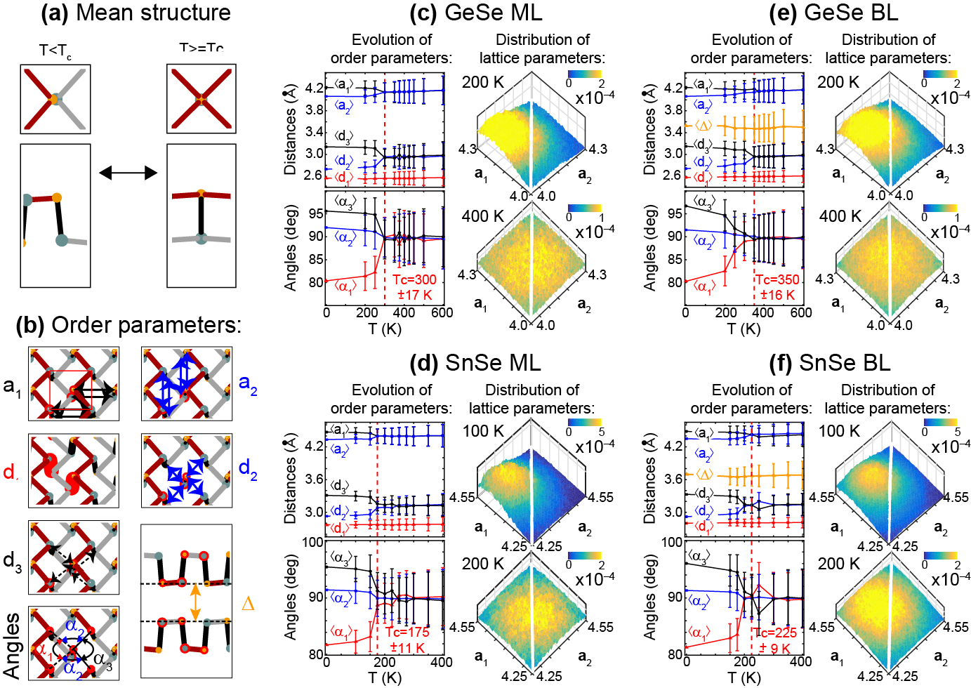
Theoretical results based on density-functional theory in Refs. Tritsaris et al. (2013); Singh and Hennig (2014); Zhu et al. (2015); Gomes and Carvalho (2015); Rodin et al. (2016); Fei et al. (2015); Cook et al. ; Morimoto and Nagaosa ; Wu and Zeng (2016); Wang and Quian correspond to structures at displayed in Fig. 1(a), and belong at the far left on the structure vs. T plots in Figs. 1(c)-(f). We performed Car-Parrinello molecular dynamics (MD) calculations at finite Soler et al. (2002); Car and Parrinello (1985); Parrinello and Rahman (1980); Junquera et al. (2001); Berland and Hyldgaard (2014) on ML and AB-stacked bilayer (BL) supercells containing up to 512 atoms, with pseudopotentials and basis sets carefully validated Rivero et al. (2015), that led to the structural evolution at finite presented in Fig. 1(c-f). In order to focus on the results, thorough descriptions of methods, as well as the full time-evolution of the instantaneous , total energy , in-plane stress, and order parameters at selected target temperatures are provided as Supplemental Material (SM, Section I).
In Fig. 1(a) we illustrate a 2D structural transition whereby a rectangular unit cell with three-fold coordinated atoms at turns onto a square unit cell with five-fold coordinated atoms at . The transition is captured in Figs. 1(c)-(f) by the thermal evolution of structural order parameters shown in Fig. 1(b) that include (i) lattice constants and , obtained in four (eight) inequivalent ways in MLs (BLs) at any given unit cell, (ii) interatomic distances up to third nearest neighbors (, and ), and (iii) angles subtended among a given atom and its second-nearest neighbors (), third-nearest neighbors () and second- and third-nearest neighbor ().
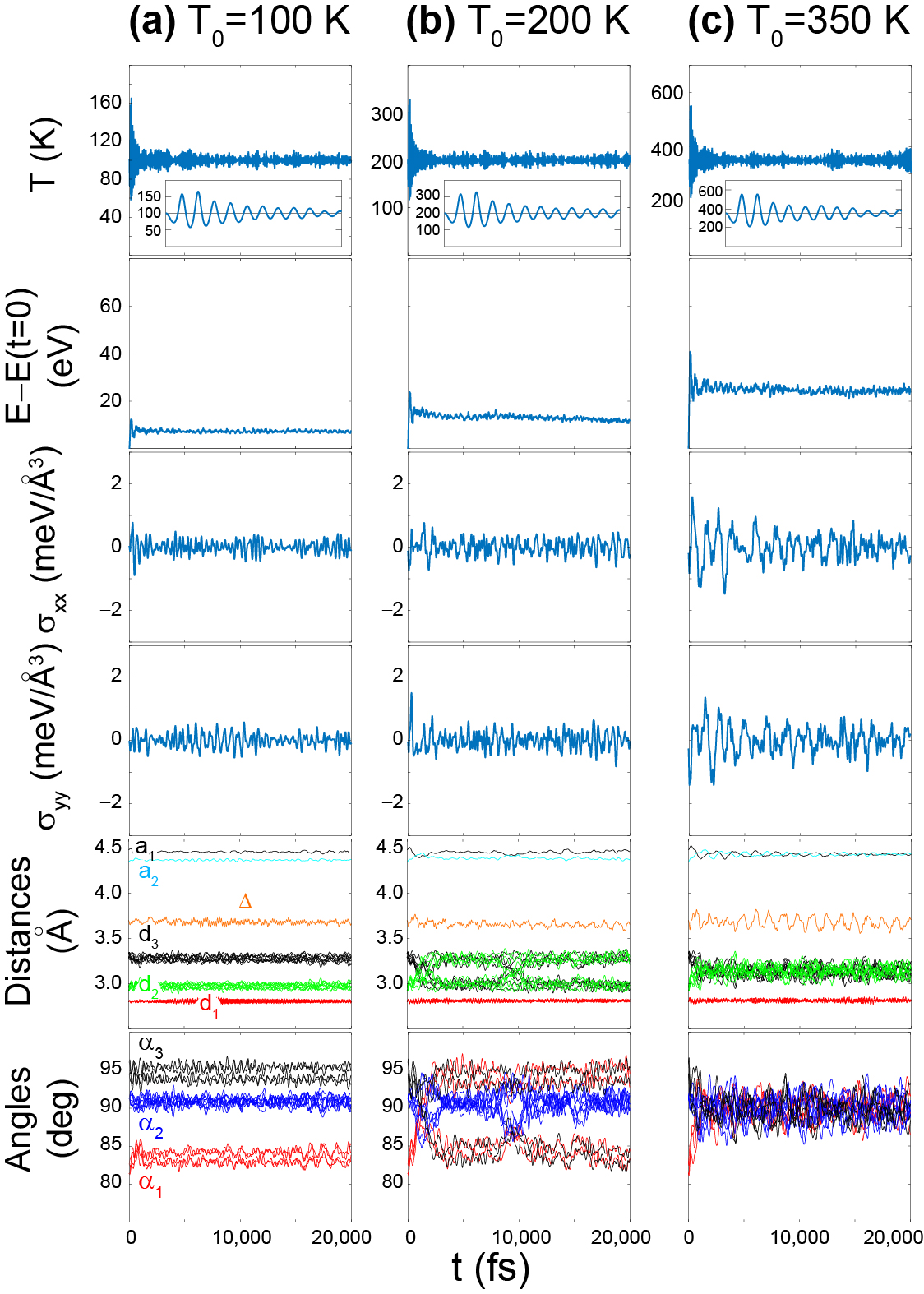
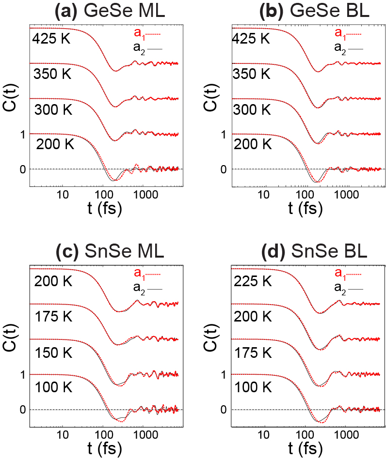
The time auto-correlation of order parameters and –a measure of the time scale of structural fluctuations– vanishes within 800 fs (Fig. 5, SM). Ensemble averages obtained from trajectories over 15,000 fs after thermal equilibration are reported in Figs. 1(c-f) for , , , and ().
Sudden changes of structural order parameters signal the transition temperature : at K, and the transition is signaled by a rapid decay of onto unity. This ratio of lattice parameters decreases with increasing atomic number, so that SnSe MLs are expected to have a smaller than GeSe MLs Mehboudi et al. (2016). Additional signatures of the transition are the coalescence of and onto a single value, and the coalescence of in-plane angles defined in Fig. 1(b) toward 90o. As seen in Fig. 1, the transition occurs at K for SnSe MLs and at a higher temperature of K for GeSe MLs. It is interesting to note that the square unit cell –corresponding to a point of unstable equilibrium at 0 K Li et al. (2015); Mehboudi et al. (2016)– becomes, on average, the preferred structure at .
Now, is known to increase with the number of layers for a given layered monochalcogenide as well Gomes and Carvalho (2015) and, accordingly, one should expect an increase of for a given material in going from MLs to BLs. Within the temperature resolution of 25 K employed in our calculations, we see a 50 K increase of in going from MLs to BLs. Such increase makes our results consistent with experiments on bulk SnSe, where is of the order of 800 K Chattopadhyay et al. (1986); Zhao et al. (2014); Li et al. (2015); Heremans (2015) (MD simulations of bulk samples require inclusion of four monolayers and are out of our reach). The structural change discussed on this and previous paragraph should be experimentally observable with XRD techniques.

We note that a melting transition would be signaled by an isotropic increase of interatomic distances , and . But the mean (inter-sublayer) distance in Figs. 1(c)-(f) remains constant through the transition, displaying smaller fluctuations than (intra-sublayer) distances and , so that individual MLs retain their 2D character through the transition. An additional (geometrical) argument for the 2D character of the transition can be made from () too: add up to . The angle defect, defined as , is equal to zero only on a planar structure Sanjuan et al. (2014).
Structural degeneracies lead to an anharmonic elastic energy profile Mehboudi et al. (2016) and hence to soft (“floppy”) phonon modes on monochalcogenide layered materials Zhao et al. (2014); Li et al. (2015); Heremans (2015); anharmonicity makes it relevant to discuss fluctuations. The distribution of lattice parameters shown at the right subplots in Figs. 1(c)-(f) for increasing has a mean value converging towards the (white) diagonal line at , which is consistent with a displacive transition Li et al. (2015). The maximum height of the distribution decays sharply nevertheless, making the distribution extremely broad as temperature raises. This broad distribution sets the error bar on and and is a signature of atomistic fluctuations (disorder). Excursions of and towards the right of the white line gain a finite probability with increasing temperature, and and have a rather homogeneous distribution at : this distribution highlights the fluctuations of the order parameter. Considering these fluctuations, material properties to be discussed next were evenly sampled out of one hundred and fifty individual frames at times fs ().
These materials remain semiconducting through the transition: the electronic density of states (DOS) obtained on instantaneous supercells at times in Fig. 2 shows a well-defined bandgap for below and above (details of DOS calculations are disclosed in SM). The bandgaps in Fig. 2 –whose magnitudes are explicitly reported in Table I (SM)– change by about 200 meV at 400 K with respect to their values at 0 K. The DOS has two additional features: (i) the sharpest peaks at 0 K that become blurred at increasing and (ii) shallow DOS pockets around the valence-band maximum for .

The band structures in Fig. 2 were obtained from instantaneous unit cells built from average lattice and basis vectors at times defined above. The width of these bands is another experimentally-observable indicator of structural fluctuations that must be visible on ARPES data. The sharp peaks in the DOS at 0 K correspond to relatively flat bands located around the point whose energy location fluctuates with increasing , thus making these peaks shallower. A band unfolding scheme Boykin and Klimeck (2005); Popescu and Zunger (2010); Lee et al. (2013); Ferrer et al. (2014) confirms these findings.
2D materials with reduced structural symmetries originate a novel paradigm in valleytronics in which crystal momentum labels individual valleys one-to-one Rivero et al. (2014). In SnSe and GeSe MLs and BLs, the shallow DOS pocket at 0 K () corresponds with a hole-valley () located along the line in Fig. 2 Tritsaris et al. (2013); Singh and Hennig (2014); Gomes and Carvalho (2015) that lies at a higher energy when contrasted to the hole-valley at the line ().
Band structure insets in Fig. 2 show the effect of on valley spin polarization that arises due to spin-orbit coupling (SOC) Fernandez-Seivane et al. (2006). The spin-polarization at these insets becomes drastically degraded at because spin-up (solid black) and spin-down (dashed yellow) bands become broader and closer together. For this reason, the remaining results on this Letter will neglect the effect of SOC. (AB BLs have zero spin polarizations at individual valleys due to inversion symmetry.)
As shown thus far, MLs and BLs increase their structural symmetry as is approached from below (Fig. 1). This means that the and points in reciprocal space –which were inequivalent for – become equivalent for as . As is reached, the hole valley along the direction raises up to align with the valley located along the line (Fig. 2). One valley contributes to the hole conductivity at the band edge for , while two valleys contribute at , giving rise to an anomalous thermal dependence of the hole conductivity at that should be visible in standard transport measurements of gated or hole-doped samples.
As seen in Fig. 3(a), crystal momentum couples to the orientation of adsorbed linearly polarized light Rodin et al. (2016). But the induced equivalence among the and points for makes the optical adsorption band edges for horizontally- and vertically-polarized light identical, making the band edge polarized at 45o, which then represents an additional optical signature of the structural transition.
The binary composition of MLs and the asymmetry upon inversion about an axis parallel to originates a net electric dipole along the longest lattice vector () Zhu et al. (2015), resulting in a piezoelectric response at 0 K Fei et al. (2015); Gomes et al. (2015). But as , and fluctuate (Fig. 1(c-f)), the orientation of these dipoles randomizes at , turning the net electric dipole moment to zero. This hypothesis is demonstrated in Fig. 3(b) by averaging the mean electric dipole moment King-Smith and Vanderbilt (1993); Kresse and Furthmüller (1996); Perdew et al. (1996); Blochl (1994); Kresse and Joubert (1999) over times at a given on instantaneous average unit cells (section VI, SM).
The three salient features of ferroelectrics are: (i) piezoelectricity, (ii) ferroelectricity, and (iii) pyroelectricity. The abrupt decay of around was fitted to sigmoidal functions, whose temperature derivative is the pyroelectric response given at lower subplots in Fig. 3(b). The pyroelectricity hereby predicted may very well be a first within the field of 2D atomic materials.
To conclude, we predict a structural transition in MLs and AB BLs of GeSe and SnSe. The transitions should be observable on mean values of lattice parameters and (in-plane) distances and angles among second and third nearest neighbors (XRD). These materials remain semiconductors through the transition, which should also be observable through ARPES, hole conductivity, and optical absorption measurements. We contributed the pyroelectric response of GeSe and SnSe MLs as well. These theoretical results may motivate and guide future experimental work in these few-layer materials with detailed thermal control and performed on an inert atmosphere.
M.M. and S.B.-L. are funded by an Early Career Grant from the DOE (Grant DE-SC0016139). Y. Y. and L. B. were funded by ONR Grant N00014-12-1-1034, and BMF by NSF DMR-1206515 and CONACyT (Mexico). J.F. acknowledges funding from the Spanish MICINN, Grant FIS2012-34858, and European Commission FP7 ITN MOLESCO (Grant 606728). Calculations were performed at Arkansas’ Trestles.
I Supplementary material
I.1 Details of molecular dynamics calculations
GeSe and SnSe monolayers (MLs) and bilayers (BLs) were studied with NPT Carr-Parrinello molecular dynamics (MD) runs on a fixed number of particles at finite temperature with the SIESTA DFT code. Calculations were performed on 88 supercells, for up to 20,000 fs, with a 1.5 fs time resolution, and employed standard basis sets, pseudopotentials with van der Waals corrections of the Berland-Per Hyldgaard type.
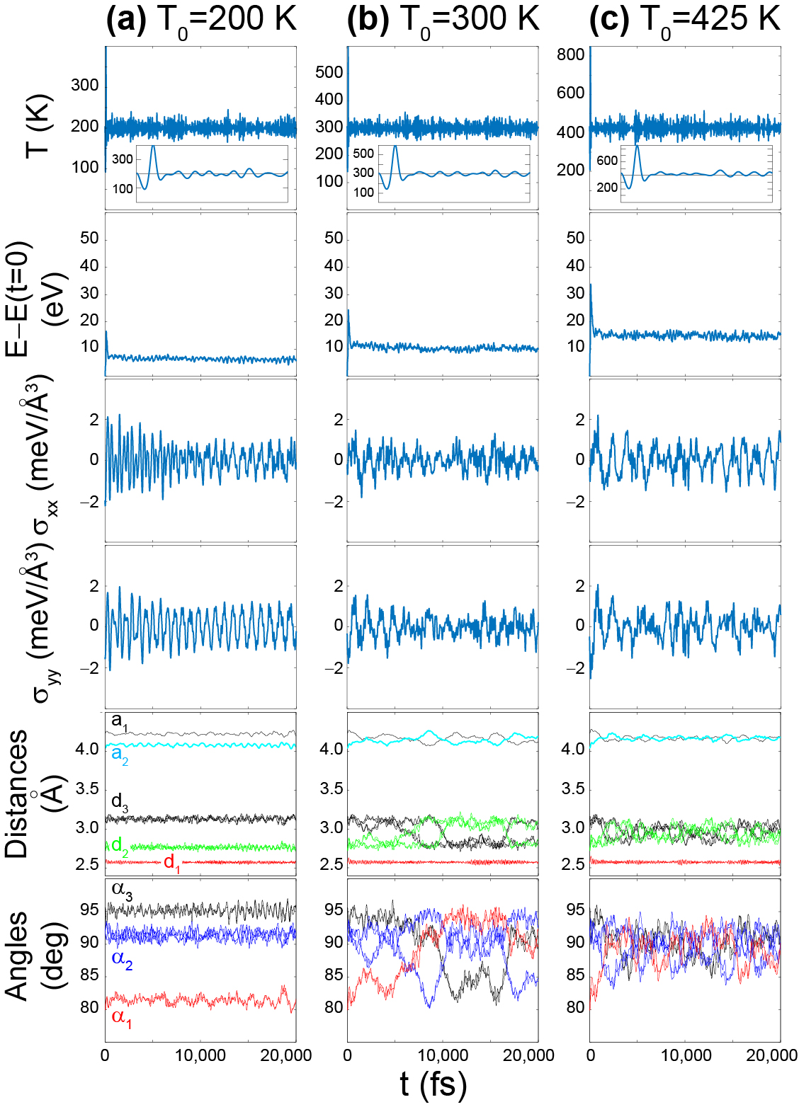
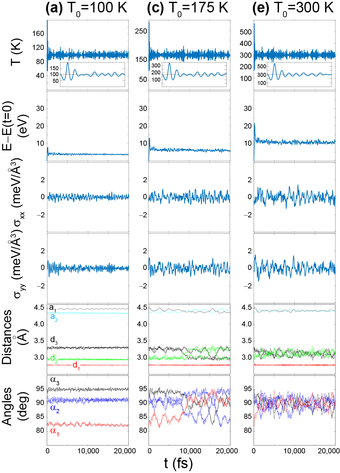
Timely execution of MD calculations requires an appropriate choice of running parameters. For a fixed number of atoms, basis set, and time resolution for the MD calculation, the crucial parameters determining speed are: (a) the point sampling, (b) the target precision of the self-consistent electronic density cycle, and (c) the fineness of the real-space grid on which the Poisson equation is solved.
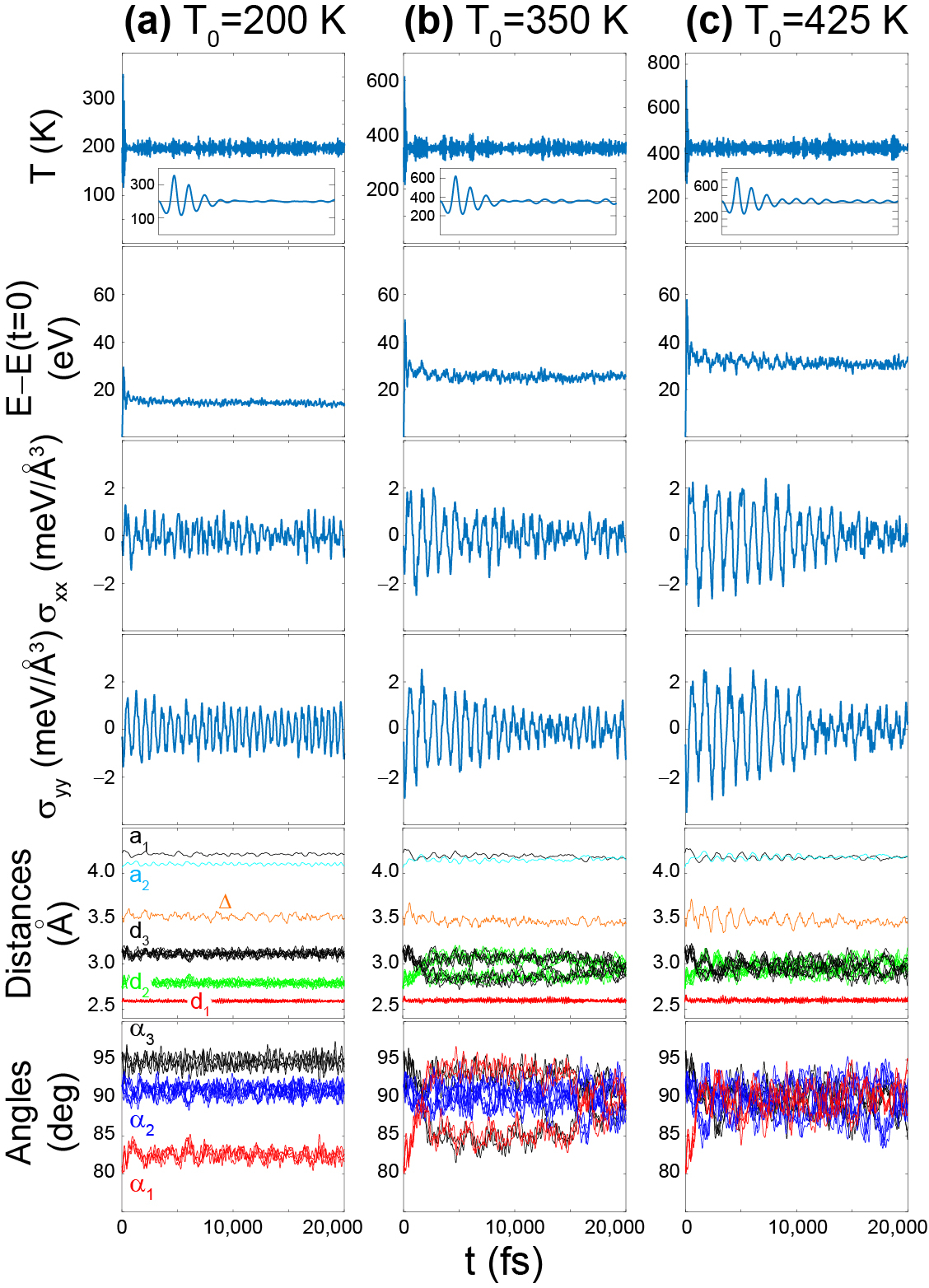
We track the temperature , the total Kohn Sham energy , the in-plane components of the stress tensor and , and structural parameters that include lattice constants, interatomic distances, and angles as a function of time (see Figs. 4 through 7, and Fig. 1(a) for graphical definitions).
Our initial choice of relevant input parameters included: (a) a point sampling of these supercells, (b) a standard precision of the electronic density equal to 10-4, and (c) a real space grid with a cutoff of 300 Ry. We call these “high-precision calculations,” which were ran at K for GeSe and SnSe MLs and BLs.
We also ran calculations at K for up to 3000 fs using the following parameters: (a) a point sampling of the supercells (i.e., a sampling that only includes the point), (b) a precision of the electronic density equal to , and (c) a real space grid with a cutoff of 150 Ry. We call these “normal precision calculations.”
We determined the sensitivity of the MD algorithm to minute changes on interatomic (Hellmann-Feynman) forces arising from these two choices of input parameters. In test runs for up to 1,000 fs and K, we find that , , and , lattice constants, interatomic distances, and angles overlap when using both sets of input parameters: runs employing “normal” parameters display an evolution of all relevant physical parameters that are essentially identical to those from runs with “high precision” parameters. Nevertheless, they accrue significantly smaller walltimes that at the end make a detailed temperature sampling possible within our computing constraints. The main results reported in this work were obtained with MD runs that employed “normal precision” parameters.
I.2 Time auto-correlation of lattice parameters
We next determine the time auto-correlation function, which applied to the lattice constants () has the following form:
| (1) |
As shown in Fig. 8, the 2D materials studied here display a vanishing time auto-correlation of about 800 fs.
| T (K) | 0 | 200 | 400 |
|---|---|---|---|
| GeSe ML | 11950 | 102053 | 94943 |
| GeSe BL | 11040 | 107622 | 100540 |
| SnSe ML | 10960 | 91530 | 85438 |
| SnSe BL | 9090 | 87425 | 79739 |
| T (K) | 0 | 200 | 400 |
|---|---|---|---|
| GeSe ML | 11950 | 111533 | 106632 |
| GeSe BL | 11040 | 108315 | 104941 |
| SnSe ML | 13290 | 95737 | 93135 |
| SnSe BL | 9100 | 89319 | 83528 |
I.3 Details of DOS calculations and Evolution of the electronic bandgaps with temperature
DOS calculations were performed on supercell structures at times defined in the main text; we employed a sampling of 30301, a tolerance of the electronic density of , a Mesh cutoff of 300 Ry, and an energy resolution of 0.01 eV. The overall sum of individual DOS traces is shown as area DOS plots in Figure 2. Band structure plots were created from the instantaneous supercell averages of lattice parameters and basis atoms at times as well. There is a small fluctuation of the horizontal axis on bands plots that is a consequence of fluctuations of and that is neglected in Fig. 2 for simplicity.
An unfolding scheme developed for DFT calculations based on numerical atomic orbitals confirmed the band structures displayed on Fig. 2.
The numerical magnitude of the DFT bandgaps and energies for direct optical transitions at the valley band edges are reported in Tables I to III. The valence band of the valley located along the symmetry line moves upward in energy as and become equal in magnitude, making that transition energy decrease in a sudden manner for .
The bands that include the effect of spin-orbit coupling, shown as insets to Fig. 2 were obtained with the Oviedo version of the SIESTA code.
| T (K) | 0 | 200 | 400 |
|---|---|---|---|
| GeSe ML | 15970 | 131889 | 103661 |
| GeSe BL | 14690 | 132545 | 104440 |
| SnSe ML | 10960 | 94764 | 90536 |
| SnSe BL | 11120 | 95840 | 84233 |
I.4 Calculation of dipole moments
The binary composition of these materials, and the inversion-asymmetric orientation of individual atoms at the unit cell creates an electric dipole in MLs that is oriented parallel to the longest lattice vector (), resulting in a piezoelectric response at 0 K.
But the orientation of these dipoles random at and the net magnitude of the electric dipole moment equal to zero. This hypothesis is demonstrated in Fig. 3(b) by computing the mean dipole over twelve average unit cells at a given temperature and without any additional optimization of the basis vectors. This was accomplished by feeding the instantaneous structural averages into the VASP code with PBE PAW pseudopotentials. In working with instantaneous averaged unit cells, we trade a spatial inhomogeneity by a temporal one. And as is approached, the relative orientation of the instantaneous average orientation among the atoms in the unit cell fluctuates, and with it the orientation of the dipole moment. The total moment decreases significantly as a result.
References
- Tritsaris et al. (2013) G. A. Tritsaris, B. D. Malone, and E. Kaxiras, J. Appl. Phys. 113, 233507 (2013).
- Singh and Hennig (2014) A. K. Singh and R. G. Hennig, Appl. Phys. Lett. 105, 042103 (2014).
- Zhu et al. (2015) Z. Zhu, J. Guan, D. Liu, and D. Tománek, ACS Nano 9, 8284 (2015).
- Gomes and Carvalho (2015) L. C. Gomes and A. Carvalho, Phys. Rev. B 92, 085406 (2015).
- Fei et al. (2015) R. Fei, W. Li, J. Li, and L. Yang, Appl. Phys. Lett. 107, 173104 (2015).
- (6) A. M. Cook, B. M. Fregoso, F. de Juan, and J. E. Moore, ArXiv:1507.08677 [cond-mat.mes-hall].
- (7) T. Morimoto and N. Nagaosa, ArXiv:1512.00549 [cond-mat.mes-hall].
- Gomes et al. (2015) L. C. Gomes, A. Carvalho, and A. H. Castro Neto, Phys. Rev. B 92, 214103 (2015).
- Mehboudi et al. (2016) M. Mehboudi, A. M. Dorio, W. Zhu, A. van der Zande, H. O. H. Churchill, A. A. Pacheco-Sanjuan, E. O. Harriss, P. Kumar, and S. Barraza-Lopez, Nano Lett. 16, 1704 (2016).
- Wu and Zeng (2016) M. Wu and X. Zeng, Nano Lett. 16, 3236 (2016).
- (11) H. Wang and X. Quian, ArXiv:1606.04522 [cond-mat].
- Rivero et al. (2014) P. Rivero, J.-A. Yan, V. M. García-Suárez, J. Ferrer, and S. Barraza-Lopez, Phys. Rev. B 90, 241408 (2014).
- Rodin et al. (2016) A. S. Rodin, L. C. Gomes, A. Carvalho, and A. H. Castro Neto, Phys. Rev. B 93, 045431 (2016).
- Soler et al. (2002) J. M. Soler, E. Artacho, J. D. Gale, A. Garcia, J. Junquera, P. Ordejon, and D. Sanchez-Portal, J. Phys.: Condens. Matter 14, 2745 (2002).
- Car and Parrinello (1985) R. Car and M. Parrinello, Phys. Rev. Lett. 55, 2471 (1985).
- Parrinello and Rahman (1980) M. Parrinello and A. Rahman, Phys. Rev. Lett. 45, 1196 (1980).
- Junquera et al. (2001) J. Junquera, O. Paz, D. Sánchez-Portal, and E. Artacho, Phys. Rev. B 64, 235111 (2001).
- Berland and Hyldgaard (2014) K. Berland and P. Hyldgaard, Phys. Rev. B 89, 035412 (2014).
- Rivero et al. (2015) P. Rivero, V. M. Garcia-Suarez, D. Pereniguez, K. Utt, Y. Yang, L. Bellaiche, K. Park, J. Ferrer, and S. Barraza-Lopez, Comp. Mat. Sci. 98, 372 (2015).
- Li et al. (2015) C. W. Li, J. Hong, A. F. May, D. Bansal, S. Chi, T. Hong, G. Ehlers, and O. Delaire, Nat. Phys. 11, 1063 (2015).
- Chattopadhyay et al. (1986) T. Chattopadhyay, J. Pannetier, and H. V. Schnering, J. Phys. Chem. Solids 47, 879 (1986).
- Zhao et al. (2014) L.-D. Zhao, S.-H. Lo, Y. Zhang, H. Sun, G. Tan, C. Uher, C. Wolverton, V. P. Dravid, and M. G. Kanatzidis, Nature 508, 373 (2014).
- Heremans (2015) J. P. Heremans, Nature Physics 11, 990 (2015).
- Sanjuan et al. (2014) A. P. Sanjuan, M. Mehboudi, E. Harriss, H. Terrones, and S. Barraza-Lopez, ACS Nano 8, 1136 (2014).
- Boykin and Klimeck (2005) T. B. Boykin and G. Klimeck, Phys. Rev. B 71, 115215 (2005).
- Popescu and Zunger (2010) V. Popescu and A. Zunger, Phys. Rev. Lett. 104, 236403 (2010).
- Lee et al. (2013) C.-C. Lee, Y. Yamada-Takamura, and T. Ozaki, Journal of Physics: Condensed Matter 25, 345501 (2013).
- Ferrer et al. (2014) J. Ferrer, C. J. Lambert, V. M. Garcia-Suarez, D. Z. Manrique, D. Visontai, L. Oroszlany, R. Rodriguez-Ferradas, I. Grace, S. W. D. Bailey, K. Gillemot, H. Sadeghi, and L. A. Algharagholy, New J. Phys. 16, 093029 (2014).
- Fernandez-Seivane et al. (2006) L. Fernandez-Seivane, M. A. Oliveira, S. Sanvito, and J. Ferrer, Journal of Physics: Condensed Matter 18, 7999 (2006).
- King-Smith and Vanderbilt (1993) R. D. King-Smith and D. Vanderbilt, Phys. Rev. B 47, 1651 (1993).
- Kresse and Furthmüller (1996) G. Kresse and J. Furthmüller, Phys. Rev. B 54, 11169 (1996).
- Perdew et al. (1996) J. Perdew, K. Burke, and M. Ernzerhof, Phys. Rev. Lett. 77, 3865 (1996).
- Blochl (1994) P. E. Blochl, Phys. Rev. B 50, 17953 (1994).
- Kresse and Joubert (1999) G. Kresse and D. Joubert, Phys. Rev. B 59, 1758 (1999).