Reconfigurable quadruple quantum dots in a silicon nanowire transistor
Abstract
We present a novel reconfigurable metal-oxide-semiconductor multi-gate transistor that can host a quadruple quantum dot in silicon. The device consist of an industrial quadruple-gate silicon nanowire field-effect transistor. Exploiting the corner effect, we study the versatility of the structure in the single quantum dot and the serial double quantum dot regimes and extract the relevant capacitance parameters. We address the fabrication variability of the quadruple-gate approach which, paired with improved silicon fabrication techniques, makes the corner state quantum dot approach a promising candidate for a scalable quantum information architecture.
Semiconductor quantum bits relying on the charge or spin degree of freedom of a single electron, bound to a quantum dot (QD) or impurity atom, are considered promising candidates for the base elements of solid state quantum computing architectures Zwanenburg et al. (2013). Building a successful quantum computer, however, requires a scalable multi-qubit approach to implement the necessary algorithms DiVincenzo (2000). Electron spins bound to silicon QDs are seen as promising candidates for this due to their long coherence time, electrical tunability and flexible coupling geometries Veldhorst et al. (2014); Kim et al. (2014); Veldhorst et al. (2015). A further advantage of using Si is the possibility to integrate with current complementary-metal-oxide-semiconductor (CMOS) technology Angus et al. (2007); Veldhorst et al. (2015); Pla et al. (2013); Crippa et al. (2015) and leverage its established industrial platform for large scale circuits. Recently, the integration of Si quantum dots and double quantum dots (DQD) into CMOS technology has been taken a step further with reports of few-electron QDs, DQDs, and donor-QD hybrids created within industry-standard Si nanowire transistors Voisin et al. (2014); Betz et al. (2015); Gonzalez-Zalba et al. (2015); Urdampilleta et al. (2015). Combined with a gate-based readout scheme that alleviates the need for a separate charge sensor Colless et al. (2013); Gonzalez-Zalba et al. (2015); Betz et al. (2015); Urdampilleta et al. (2015); Gonzalez-Zalba et al. (2016) these approaches pave the way towards a large scale quantum computing architecture based on current CMOS technology.
In this Letter, we report on a reconfigurable QD and DQD system in a quadruple-gate CMOS transistor. It incorporates one, or a pair, of CMOS corner state quantum dots Betz et al. (2015); Gonzalez-Zalba et al. (2015) in a variety of configurations.
Each of the four gates can host an independently tunable quantum dot created in the square channel by electrostatic enhancement and confinement resulting from the top-gate electrodes and accompanying silicon nitride spacers. We characterise one exemplary single QD and demonstrate that different DQD configurations can be set at will. Building on previous demonstrations Betz et al. (2015); Gonzalez-Zalba et al. (2015); Urdampilleta et al. (2015), our results provide a way to scale up CMOS quantum information architectures and to create reconfigurable silicon multi-dot arrangements.
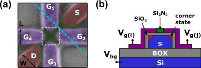
The device presented here is a fully depleted silicon-on-insulator (FDSOI) nanowire field-effect transistor with four independently addressable top-gates. The poly-silicon top-gates of length are arranged around the sides of a square at with respect to transport direction as shown in white dashes in the scanning electron micrograph of a similar device in Fig.1(a). Gate-to-gate distances are , and the channel width is . Fig.1(a) shows the Si3N4 spacers deposited between the gates and extending towards source and drain in green. The channel below remains undoped generating the source, drain and inter-dot tunnel barriers. Fig.1(b) shows a cross-section sketch of the device perpendicular to the direction of transport, taken at the line indicated by the cyan line in Fig.1(a). The device comprises an Si back plane serving as global backgate, topped by a SiO2 buried oxide. This is followed by the undoped, square Si (001) channel of thickness , which is achieved by etching down the SOI substrate prior to gate stack deposition. Each top-gate wraps around two faces of the intrinsic channel and is separated from the other top-gates by the Si3N4 spacers and from the channel by of SiO2 Hofheinz et al. (2006). A quantum dot can be created under each gate at the top-most corners of the channel due to the so-called corner effect Sellier et al. (2007); Gonzalez-Zalba et al. (2015); Betz et al. (2015). Each QD is controlled by its respective gate voltage , while a global backgate voltage may be applied through the Si substrate. All measurements shown in this Letter are in direct transport and unless otherwise stated were taken at , to enhance the dot-to-dot and dot-to-lead couplings Roche et al. (2012).
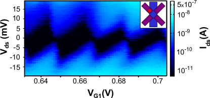
Corner state quantum dots in Si nanowire transistors have been reported for different single and double gate topologies Betz et al. (2015); Gonzalez-Zalba et al. (2015); Voisin et al. (2014) and using both quantum dots and dopants Urdampilleta et al. (2015). In our novel quadruple gate configuration, we first of all confirm the creation of a single QD under a top-gate using gate as an example. In order to allow for a source-drain current, is pulled high above threshold to , while the gates on the opposite channel side remain well below threshold at . The backgate voltage is set to . This provides a single QD under gate , as can be seen from the stability map of Fig.2. We extract a charging energy and source and drain capacitances and from the slope of the Coulomb diamonds and the gate voltage period. Single QDs embedded in a multi-gate structure like the one investigated here could host single electron spin qubits, or be used as single-electron transistors for charge detection of a nearby dot.
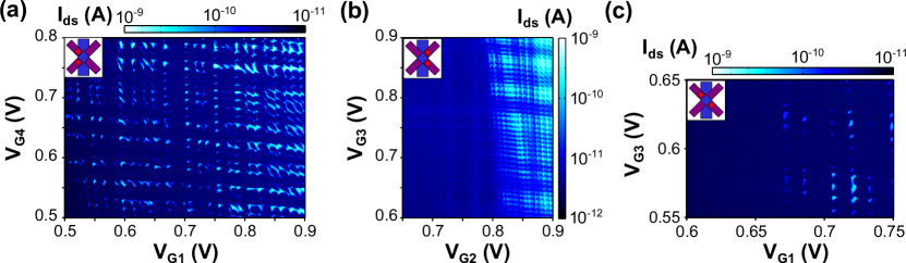
The ability to create multi-QD configurations is, as mentioned above, an important ingredient in the pursuit of a scalable semiconductor QIP architecture. In the following paragraphs we demonstrate that different configuration of serial DQDs can be formed in the nanowire transistor and extract the DQD coupling capacitances. All following measurements were carried out at a small source-drain voltage . First of all, we configure the device as a serial DQD on the - axis, by setting . Fig.3(a) shows the resulting DC current as a function of and . In the stability map, we observe a honeycomb pattern and at its vertices we find the so-called bias triangles, i.e. periodic regions of enhanced current resulting from the alignment of both QD energy levels within the bias window, indicative of a serial DQD van der Wiel et al. (2002). At low voltages on both and the stability map shows the checker box behaviour characteristic for low inter-dot coupling, transitioning to the aforementioned honeycomb arrangement for intermediate coupling strength. At elevated top-gate voltages the inter-dot coupling increases, resulting in undulated diagonal lines of enhanced conductance indicating that the QDs are strongly tunnel coupled Lai et al. (2011). The voltage spacing of Coulomb oscillations in the low to intermediate coupling regime is and (see also Fig.4(a)). Both spacings are very regular across the voltage range studied here, indicating stable QD position and size.
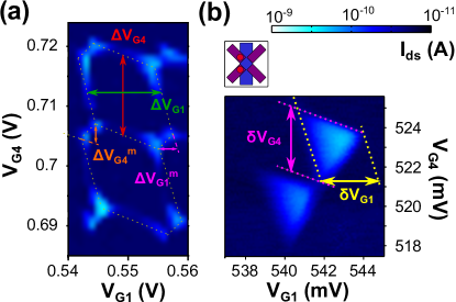
Fig.3(b) presents the opposite configuration to Fig.3(a), a serial DQD along - with now . Similarly to Fig.3(a) we obtain a honeycomb diagram, albeit a more compressed one with and , indicating larger QDs. Finally, Fig.3(c) shows the stability map for a diagonal DQD using and as constituent quantum dots. Here, the overall current is reduced compared to the previous two configurations, which we attribute to the larger distance between the dots under and and hence reduced iter-dot tunnel rates. We extract Coulomb spacings and , approximately in line with the previous results. Similar results have been obtained for the DQD along the - axis (not shown here).
Last but not least, we study the serial DQD along - in more detail to obtain estimates of the capacitances involved in the system. From the honeycomb diagram outlined in Fig.4(a) we extract voltage spacings and between Coulomb oscillations. These spacings are linked to the gate capacitances of the two serial QDs as van der Wiel et al. (2002) and we thus estimate and . Applying this analysis to the - configuration, we find gate capacitances and . The voltage spacings and extracted from Fig.4(b) in combination with the source-drain voltage provide us with an estimate for the lever arms and total capacitances as van der Wiel et al. (2002). We find lever arms and total capacitances . These values in addition to from Fig.4(a) allow us now to also approximate the mutual capacitance linking the QDs under gates and : . The same analysis carried out for the diagonal DQD along - (not shown here) yields a mutual capacitance .
Variability between nominally identical devices from different batches but also within a single batch fabricated at the same time is an important benchmarking parameter in CMOS technology. Comparing all four gate capacitances of the device presented here, we find a mean gate capacitance of about and a variance of . We attribute this variance to variations in gate dielectric thickness and quality, as well as gate misalignment relative to the channel. All three factors directly influence the enhancement mode corner state QDs.
In conclusion, we have demonstrated a reconfigurable quantum dot and double quantum dot system based on a quadruple-gate CMOS transistor.
Taking into account the continuous improvement of CMOS fabrication techniques and the single electron control demonstrated here, corner state quantum dots present a valid and scalable option as base elements of a silicon quantum information architecture.
Moreover, this approach can readily be extended to a larger number of gates providing a 1-D line of QDs and DQDs,while remaining compact by further integrating high-sensitivity gate-based reflectometry readout Gonzalez-Zalba et al. (2015); Betz et al. (2015). The versatility of the corner state QD structure allows to use the gate-based sensing either for in-situ readout, but also for conventional charge sensing using an rf-single electron box for detection. Further experiments that can be envisioned with this architecture are e.g. electron charge and electron spin buses, measurements of long distance coherent coupling Braakman et al. (2013), and single spin CCD Baart et al. (2015).
The authors thank D.A. Williams and M. Fanciulli for support and discussion. The research leading to these results has been supported by the European Community’s seventh Framework under the Grant Agreement No. 214989. The samples presented in this work were designed and fabricated by the AFSID project partners (www.afsid.eu). A.J. Ferguson acknowledges support from EPSRC (EP/K027018/1) and from his Hitachi research fellowship. M.L.V. Tagliaferri acknowledges support from the Short Term Mobility Program 2015 of Consiglio Nazionale delle Ricerche (CNR), Italy.
References
- Zwanenburg et al. (2013) F. A. Zwanenburg, A. S. Dzurak, A. Morello, M. Y. Simmons, L. C. L. Hollenberg, G. Klimeck, S. Rogge, S. N. Coppersmith, and M. A. Eriksson, Rev. Mod. Phys. 85, 961 (2013).
- DiVincenzo (2000) D. P. DiVincenzo, Fortschritte Der Physik 48, 771 (2000).
- Veldhorst et al. (2014) M. Veldhorst, J. C. C. Hwang, C. H. Yang, A. W. Leenstra, B. de Ronde, J. P. Dehollian, J. T. Muhonen, F. Hudson, K. M. Itoh, A. Morello, and A. S. Dzurak, Nat. Nano. , 981 (2014).
- Kim et al. (2014) D. Kim, Z. Shi, D. R. Simmons, C. B.and Ward, J. R. Prance, T. S. Koh, J. K. Gamble, D. E. Savage, M. G. Lagally, M. Friesen, S. N. Coppersmith, and M. A. Eriksson, Nature 511, 70 (2014).
- Veldhorst et al. (2015) M. Veldhorst, C. H. Yang, J. C. C. Hwang, W. Huang, J. P. Dehollian, S. Muhonen, J. T. aand Simmons, A. Laucht, F. Hudson, K. M. Itoh, A. Morello, and A. S. Dzurak, Nature 526, 410 (2015).
- Angus et al. (2007) S. J. Angus, A. J. Ferguson, A. S. Dzurak, and R. G. Clark, Nano Letters 7, 2051 (2007).
- Pla et al. (2013) J. J. Pla, K. Y. Tan, J. P. Dehollain, W. H. Lim, J. J. L. Morton, F. A. Zwanenburg, D. N. Jamieson, A. S. Dzurak, and A. Morello, Nature 496, 334 (2013).
- Crippa et al. (2015) A. Crippa, M. L. V. Tagliaferri, D. Rotta, M. De Michielis, G. Mazzeo, M. Fanciulli, R. Wacquez, M. Vinet, and P. E., Physical Review B 92, 035424 (2015).
- Voisin et al. (2014) B. Voisin, V.-H. Nguyen, J. Renard, X. Jehl, S. Barraud, F. Triozon, M. Vinet, I. Duchemin, Y.-M. Niquet, S. de Franceschi, and M. Sanquer, Nano Letters 14, 2094 (2014).
- Betz et al. (2015) A. C. Betz, R. Wacquez, M. Vinet, X. Jehl, A. L. Saraiva, M. Sanquer, A. J. Ferguson, and M. F. Gonzalez-Zalba, Nano Letters 15, 4622 (2015).
- Gonzalez-Zalba et al. (2015) M. F. Gonzalez-Zalba, S. Barraud, A. J. Ferguson, and A. C. Betz, Nature Communications 6 (2015), doi:10.1038/ncomms7084.
- Urdampilleta et al. (2015) M. Urdampilleta, A. Chatterjee, C. C. Lo, T. Kobayashi, J. Mansir, S. Barraud, A. C. Betz, S. Rogge, M. F. Gonzalez-Zalba, and J. J. L. Morton, Phys. Rev. X 5, 031024 (2015).
- Colless et al. (2013) J. I. Colless, A. C. Mahoney, J. M. Hornibrook, A. C. Doherty, H. Lu, A. C. Gossard, and D. J. Reilly, Physical Review Letters 110, 046805 (2013).
- Gonzalez-Zalba et al. (2016) M. F. Gonzalez-Zalba, S. N. Shevchenko, S. Barraud, J. R. Johansson, A. J. Ferguson, F. Nori, and A. C. Betz, Nano Letters 0, null (2016), pMID: 26866446, http://dx.doi.org/10.1021/acs.nanolett.5b04356 .
- Hofheinz et al. (2006) M. Hofheinz, X. Jehl, M. Sanquer, G. Molas, M. Vinet, and S. Deleonibus, Applied Physics Letters 89 (2006), http://dx.doi.org/10.1063/1.2358812.
- Sellier et al. (2007) H. Sellier, G. P. Lansbergen, J. Caro, S. Rogge, N. Collaert, I. Ferain, M. Jurczak, and S. Biesemans, Applied Physics Letters 90 (2007).
- Roche et al. (2012) B. Roche, B. Voisin, X. Jehl, R. Wacquez, M. Sanquer, M. Vinet, V. Deshpande, and B. Previtali, Applied Physics Letters 100, 032107 (2012), http://dx.doi.org/10.1063/1.3678042.
- van der Wiel et al. (2002) W. G. van der Wiel, S. De Franceschi, J. M. Elzerman, T. Fujisawa, S. Tarucha, and L. P. Kouwenhoven, Reviews of Modern Physics, 75, 1 (2002).
- Lai et al. (2011) N. S. Lai, W. H. Lim, C. H. Yang, F. A. Zwanenburg, W. A. Coish, F. Qassemi, A. Morello, and A. S. Dzurak, Scientific Reports 1 (2011), 10.1038/srep00110.
- Braakman et al. (2013) F. R. Braakman, P. Barthelemy, C. Reichl, W. Wegscheider, and L. M. K. Vandersypen, Nature Nanotechnology 8, 432 (2013).
- Baart et al. (2015) T. Baart, M. Shafiei, T. Fujita, C. Reichl, W. Wegscheider, and L. M. K. Vandersypen, Nature Nanotechnology (2015), 10.1038/nnano.2015.291.