Uniaxially stressed germanium with fundamental direct band gap
Abstract
We demonstrate the crossover from indirect- to direct band gap in tensile-strained germanium by temperature-dependent photoluminescence. The samples are strained microbridges that enhance a biaxial strain of 0.16% up to 3.6% uniaxial tensile strain. Cooling the bridges to 20 K increases the uniaxial strain up to a maximum of 5.4%. Temperature-dependent photoluminescence reveals the crossover to a fundamental direct band gap to occur between 4.0% and 4.5%. Our data are in good agreement with new theoretical computations that predict a strong bowing of the band parameters with strain.
pacs:
On-chip data transmission is currently the bottleneck to further increase computing power as metal wiring reaches its fundamental limits concerning band width and energy consumption Miller (2009). Hence, optical interconnects are envisioned to overcome the drawbacks of their electrical counterpart. However, the realization of an efficient light source compatible with the complementary metal-oxide-semiconductor (CMOS) environment is still the greatest challenge for the convergence of electronics and photonics on silicon. This is caused by the indirect nature of silicon‘s band gap which prohibits efficient light emission. For monolithic integration of a light source on Si it is, hence, desirable to have a material with a direct band gap but - in contrast to direct gap III-V lasers heterogeneously integrated on Si Fang et al. (2008) - with chemical compatibility to Si. In this respect, Ge has gained a lot of attention due to its CMOS compatibility and its small conduction band offset between the direct and the indirect L states of only 140 meV. To close this offset and transform Ge into a direct band gap semiconductor, the application of tensile strain Süess et al. (2013); Ghrib et al. (2015); Capellini et al. (2014) as well as alloying Ge with Sn Wirths et al. (2015); Chen et al. (2013); Gallagher et al. (2015) have become a very active field of research. The recent observation of lasing in a high Sn-content partially strain-relaxed GeSn-alloy with a band offset of minus 25 meV (i.e. minimum of -valley below the energy of the L-valleys) delivered a proof of concept for direct band gap group IV light emitters Wirths et al. (2015). However, lasing was so far limited to a maximum temperature of 90 K due to the rapidly decreasing non-radiative lifetime of only a few hundred picoseconds at temperatures 100 K Wirths et al. (2015). Direct band gap elemental Ge of high quality would, in contrast, take full advantage from longer non-radiative recombination times enabling lasing at elevated temperatures given that a similar conduction band offset can be achieved. However, in spite of the many efforts to reach a direct band gap configuration in Ge by applying tensile strain, there is still the lack of proving a fundamental direct band gap as spectroscopy on structures with a sufficiently high strain was either not presented Sukhdeo et al. (2014) or performed only at room temperature Ghrib et al. (2015); Sánchez-Pérez et al. (2011), which is not sufficient to substantiate the claim.
In this letter, we present Ge microstructures fabricated from high-quality optical germanium-on-insulator (GeOI) substrates where the material quality is assessed by determination of the minority carrer lifetime. By measuring temperature-dependent photoluminescence (PL) on structures with different strain and at various excitation intensities, we validate the transition from an indirect- to a fundamental direct band gap semiconductor - which manifests in a strong direct gap emission at 20 K - to occur for Ge with a uniaxial strain between 4.0% and 4.5%.
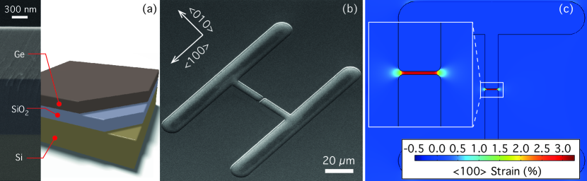
To introduce a high tensile stress in Ge, we make use of stress-enhancement by geometrical patterning as introduced in ref. Süess et al. (2013). GeOI serves as the starting substrate. It is obtained from a thick layer of intrinsic Ge grown on Si which gets transferred to an oxidized Si wafer using SmartCutTM technology Reboud et al. (2015). After layer transfer, the misfit dislocations originating from the defective Ge/Si interface region are located on the top of the layer stack and are, therefore, readily accessible and removed via chemical mechanical polishing (CMP). After CMP, a 1 m thick Ge layer of high quality is obtained on top of a 1 m buried oxide layer (see Fig. 1(a) and supporting material (SM) Ano ). The bonding process preserves most of the epitaxially induced strain which originates from the difference in thermal expansion coefficients between Si and Ge, leaving a biaxial tensile strain of 0.16% at room temperature after layer transfer and CMP.
Patterning of the Ge layer into 100 oriented microbridges is performed via electron beam lithography and reactive ion etching to define a central, narrow ‘constriction’ symmetrically surrounded by ‘pads’ with large cross sections Süess et al. (2013), see Fig. 1(b). When the underlying buried oxide is selectively removed with vaporous hydrofluoric acid, the pads relax which leads to a strong uniaxial tensile stress in the constriction, as accurately reproduced by finite-element COMSOL (FEM) modelling shown in Fig. 1(c). This geometrical enhancement of tensile strain can be widely tuned by choosing appropriate ratios of width and length for constriction and pads with the material‘s yield strength as the limiting parameter Süess et al. (2013).
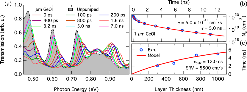
The motivation to use GeOI as starting substrate lies in the improved mechanical and optical properties compared to Ge layers directly on Si: Due to the reduced density of threading dislocations and the absence of a defective Ge/Si interface, the yield strength increases and the internal quantum efficiency of light emission rises thanks to a longer non-radiative recombination time. We extract the latter via infrared pump-probe transmission measurements at the infrared beamline X01DC of the Swiss Light Source using a 100 ps Nd:YAG laser pulse as excitation and the broadband synchrotron radiation as probe Carroll et al. (2011). In Fig. 2(a), transmission spectra through a GeOI substrate are shown for varying delay times between pump- and probe pulses. The high refractive index contrast between Ge and the buried oxide facilitates distinct Fabry-Perot (FP) interferences. The peak positions shift with a linear dependence on the optically excited charge carrier density as is proportional to , where is the refractive index Geiger et al. (2014). From the spectra shown in Fig. 2(a), the extracted charge carrier densities (blue circles) are plotted together with the fitted exponential decay (red line) in Fig. 2(b). The non-radiative lifetime as well as the Auger recombination coefficient , which relates the Auger recombination time to the carrier density as , serve as free fitting parameters, which are obtained as = 5.0 ns and = 5.010-31 cm6/s (for details see Ano ). The latter value is a factor 2 to 3 larger than compared to literature values obtained under low excitation Uleckas et al. (2011) but is about one order of magnitude lower than the Auger recombination rate as obtained under carrier saturation conditions Carroll et al. (2012) when probably also higher than second order Auger processes begin to play a role. To decouple bulk- and surface/interface effects, the lifetime is measured on samples with different thickness after thinning by reactive ion etching using SF6, Ar and CHF3 (see Fig. 2(c)). The thickness-dependent data are accurately described by
| (1) |
where is the bulk lifetime, the layer thickness, the surface recombination velocity and the diffusion constant Saito et al. (2014); Gaubas and Vanhellemont (2006); Sproul (1994). With = 100 cm2/s Young and van Driel (1982), we obtain = 5500 cm/s and a bulk lifetime of = 12.0 ns. Apparently, the dry etching does not affect the surface recombination velocity which we attribute to a passivation of the surface states with methyl groups Jiang et al. (2014).
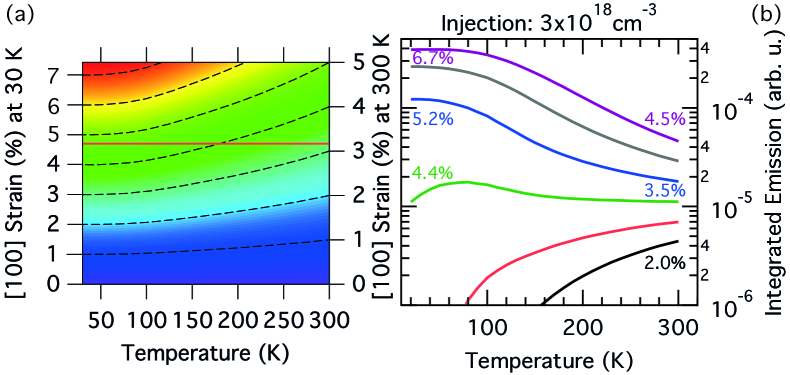
Using the unthinned GeOI material, microbridges with constrictions of 6 m 500 nm and varying pad lengths are fabricated, yielding a maximum Raman shift of -6.7 cm-1 from power-dependent Raman spectroscopy Süess et al. (2014). According to the recently determined non-linear relation between Raman shift and 100 uniaxial strain ε given in ref. Gassenq et al. , this corresponds to a strain of 3.6% at room temperature. By cooling the samples, this strain is enhanced due to the different thermal expansion coefficients of Si and Ge and the redistribution of the tensile strain in the Ge layer by , where is the enhancement factor given by the structure‘s geometry and denotes the biaxial strain in the layer. Taking into account the temperature-dependent thermal expansion coefficients of Si Okada and Tokumaru (1984) and Ge Novikova (1960), the biaxial strain in the layer increases by 0.073% to a total of 0.24% when going from 300 K down to 20 K. As shown in Fig. 3(a), the strain in a given microbridge increases accordingly. From the finite element modelling, it follows that e.g. 4.7% - which, according to deformation potential theory, appears to be the crossover to a fundamental direct band gap Geiger et al. (2015) - can already be obtained for bridge structures with a room-temperature strain of 3.2% when cooling to temperatures below 50 K as highlighted in Fig. 3(a).
Besides the increase in strain, lowering the temperature also thermalizes the electrons into the lowest energy states available in the conduction band. This effect will be exploited here to distinguish between fundamentally direct- and indirect band gap, as we have recently done for the proof of a fundamental direct band gap in GeSn Wirths et al. (2015). In Fig. 3(b), the integrated spontaneous emission intensity for direct gap transitions is calculated as a function of temperature for structures with room-temperature (RT) strain values between 2.0% and 4.5% at a constant injected carrier density of cm-3. The model takes into account the T-dependent strain increase from Fig. 3(a) with linear band shifts according to deformation potential theory Geiger et al. (2015), as well as the joint-density-of-states of the dipole-allowed transitions between the -valley and the highest valence band states, assuming isotropic, parabolic bands (see ref. Wirths et al. (2015) for details). Two regimes are found: (i) For 3.0% at RT, the direct gap – crossover cannot be reached and the electrons, hence, populate the indirect L-valleys, which does not yield efficient radiative recombination. (ii) For 3.0% at RT, however, cooling increases the population of the -valley such that the direct gap emission intensity increases.
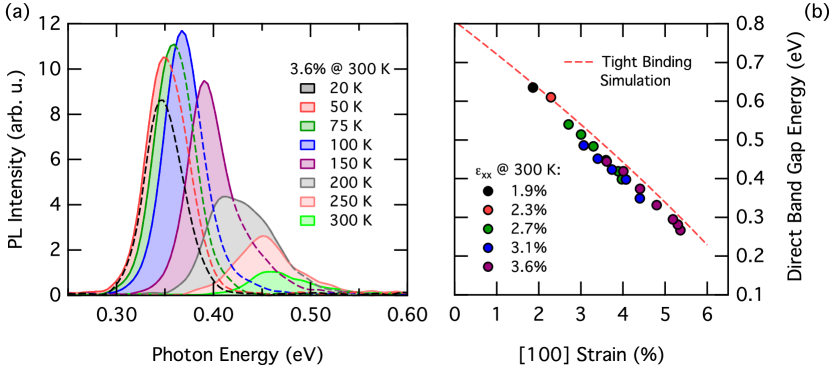
In Fig. 4(a), PL spectra of a microbridge with 3.6% strain at 300 K are shown for varying temperatures. Carriers are optically excited by a continuous-wave laser emitting at 532 nm with an incident power of 7 mW on an approximately 7 m spot corresponding to 18 kW/cm2. As expected from our model in Fig. 3(a), the strain increases for lower temperatures, leading to a red-shift in emission which overcompensates the typically observed blue-shift of the band gap. To further corroborate the validity of our temperature-dependent strain extrapolation, we extract the strain-dependent direct band gaps for a set of samples with different strain by fitting the PL peak with a simple model for the spontaneous radiative efficiency of a bulk material as
| (2) |
where is the Boltzmann constant. The obtained band gaps are shifted towards their room-temperature value using Varshni‘s formula Varshni (1967):
| (3) |
Here, = 0.88 eV (ref. Schäffler (1997)), = 4.774×10⁻⁴ 1/K (ref. Thurmond (1975)) and b = 235 K (ref. Thurmond (1975)). The extrapolation of strain values for low temperatures according to FEM simulations seems confirmed as the band gaps extracted from different structures (i.e. with different RT strain) at the same strain state show an excellent agreement (see Fig. 4(b)). It should be noted that even after several cycles of cooling, the structures show no sign of degradation and the same maximum strain is reached. In Fig. 4(b), the experimental band gap energies at are compared to those calculated with the tight-binding model and methodology of ref. Niquet et al. (2009) which was previously applied for biaxially strained Ge. This model reproduces ab initio calculations over a wide range of deformations and predicts, in particular, a bowing of band gap energy at large uniaxial strain which is found to be in good agreement with the experimental data.
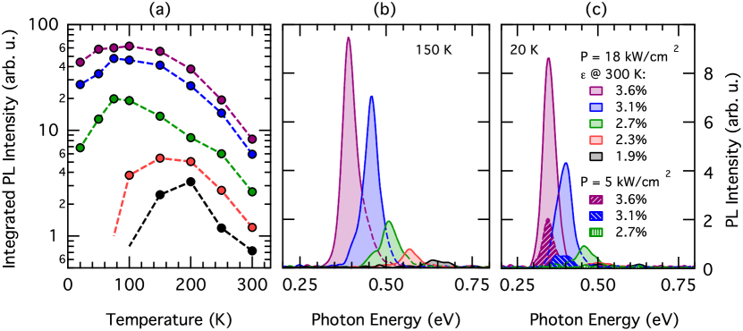
Lastly, the intensities integrated over the PL peak are plotted in Fig. 5(a) as a function of temperature for the excitation density of 18 kW/cm2. When comparing intensities between the different samples at any given temperature, higher strain yields higher emission intensity due to a progressively more favorable alignment between - and L-valleys. When cooling from 300 K down to 200 K, we observe an intensity increase for all bridges including the ones at strain below 3.0% albeit a monotonic decrease would be expected according to Fig. 3(b). We attribute this to the ambipolar carrier diffusion which helps to collect a large amount of excited carriers from the pad into the bridge region, in particular at lower temperatures (we estimate a larger carrier density to be excited outside of the constriction compared to the highly strained part, see Ano ). This experimentally observed effect Süess et al. (2013); Nam et al. (2013) is not accounted for in the model. In contrast, the faster carrier diffusion will lead to an enhanced surface recombination velocity Stevenson and Keyes (1954). However, this effect seems to be overcompensated by the carrier collection. At 150 K, direct gap emission from all samples can still be detected (see Fig. 5(b)), whereas for lower temperatures the emission for bridges with 2.7% at RT vanishes.
At 20 K, a strong direct gap emission is obtained from samples with RT strain of 2.7%, 3.1% and 3.6% translating into 4.0%, 4.5% and 5.4% at 20 K (Fig. 5(c)). Under a lower excitation density of 5 kW/cm2 which corresponds to a steady-state carrier density of 4.61017 cm-3 at a lifetime of 5.0 ns and neglecting carrier diffusion, the direct gap emission of the 4.5% and 5.4% strained bridges can still be clearly detected, while the intensity at 4.0% strain drops below the noise limit (see the shaded, filled areas in Fig. 5(c)). Therefore, samples at 4.5% and 5.4% are identified as having a fundamental direct band gap, whereas 4.0% appears to be around the transition point. The crossover of Ge towards a true direct band gap semiconductor is, hence, found between 4.0% and 4.5% uniaxial strain, which is the main outcome of this letter.
The intensity decrease for direct gap samples when cooling from 100 K to 20 K cannot be explained by above introduced model that predicts a constant PL intensity as a function of temperature in that temperature range. We ascribe this to a lower efficiency for phonon-assisted L intervalley scattering (IVS) for electrons diffusing from the outer pad regions (where the population is located in the indirect valley) into the central constriction (with its direct band gap), similar to experimental results for temperature-dependent X,L scattering times in GaAs Cavicchia et al. (1996). Due to the near-degeneracy of the - and L-valleys in the strained Ge, the IVS phonon bottleneck is more pronounced than in GaAs, which explains that in spite of the long non-radiative lifetime, the occupation of at low temperature does not seem to be in thermal equilibrium with the one of the L valley. This phonon bottleneck will disappear when the band edge is more than a typical phonon energy (30 meV) below the L states. This is exactly what we observe for the sample with the highest strain where we extrapolate that the band gap offset is approximately minus 40 meV with the decline being less than a factor of 2. For this extrapolation, we assume the crossover at 4.25 % and use a simple linear correlation, i.e. the offset value is 140 meV = -40 meV. An alternative explanation would attribute the behavior to a different coefficient in Varshni‘s law for and L states Varshni (1967), as a weaker T-dependent energy decrease for L than for would have a similar effect. However, as the band gap variations vanish towards low temperatures, the Varshni parameter-argument seems less likely for a sound explanation of the observed effect.
In summary, we have investigated strained germanium microbridges fabricated from high-quality germanium-on-insulator substrates with strain values around the transition from indirect to fundamental direct band gap. Temperature-dependent photoluminescence reveals a qualitatively different behavior depending on strain, with a vanishing direct gap emission at low temperature for 4.0% and a strong direct gap emission for higher strain. Therefore, the crossover of germanium towards an elemental group IV semiconductor with a fundamental direct band gap was evidenced at a strain between 4.0% and 4.5%. Furthermore, we have shown long carrier lifetimes in optical GeOI substrates and observed a phonon bottleneck for thermalization of the carriers from the L- into the states. Finally, our data are in agreement with a strong bowing of the band gap energy with strain as predicted by theory. In conclusion, long non-radiative lifetimes together with high mechanical stability make the newly developed GeOI substrate a most promising platform to realize an efficient direct band gap laser for monolithic integration on a Si CMOS platform.
Acknowledgements.
Parts of this work were supported by the Swiss National Science Foundation (SNF Project No. 149294) as well as by the CEA projects DSM-DRT Phare Photonics and Operando. We thank Stefan Stutz for sample preparation and the X01DC beamline of the Swiss Light Source for accessibility.References
- Miller (2009) D. A. B. Miller, Proceedings of the IEEE 97, 1166 (2009).
- Fang et al. (2008) A. W. Fang, E. Lively, Y.-H. Kuo, D. Liang, and J. E. Bowers, Optics Express 16, 4413 (2008).
- Süess et al. (2013) M. J. Süess, R. Geiger, R. A. Minamisawa, G. Schiefler, J. Frigerio, D. Chrastina, G. Isella, R. Spolenak, J. Faist, and H. Sigg, Nature Photonics 7, 466 (2013).
- Ghrib et al. (2015) A. Ghrib, M. El Kurdi, M. Prost, S. Sauvage, X. Checoury, G. Beaudoin, M. Chaigneau, R. Ossikovski, I. Sagnes, and P. Boucaud, Advanced Optical Materials 3, 353 (2015).
- Capellini et al. (2014) G. Capellini, C. Reich, S. Guha, Y. Yamamoto, M. Lisker, M. Virgilio, A. Ghrib, M. El Kurdi, P. Boucaud, B. Tillack, and T. Schroeder, Optics Express 22, 399 (2014).
- Wirths et al. (2015) S. Wirths, R. Geiger, N. von den Driesch, G. Mussler, T. Stoica, S. Mantl, Z. Ikonic, M. Luysberg, S. Chiussi, J. M. Hartmann, H. Sigg, J. Faist, D. Buca, and D. Grützmacher, Nature Photonics 9, 88 (2015).
- Chen et al. (2013) R. Chen, S. Gupta, Y.-C. Huang, Y. Huo, C. W. Rudy, E. Sanchez, Y. Kim, T. I. Kamins, K. C. Saraswat, and J. S. Harris, Nano Letters 14, 37 (2013).
- Gallagher et al. (2015) J. D. Gallagher, C. L. Senaratne, P. Sims, T. Aoki, J. Menendez, and J. Kouvetakis, Applied Physics Letters 106, 091103 (2015).
- Sukhdeo et al. (2014) D. S. Sukhdeo, D. Nam, J.-H. Kang, M. L. Brongersma, and K. C. Saraswat, Photonics Research 2, A8 (2014).
- Sánchez-Pérez et al. (2011) J. R. Sánchez-Pérez, C. Boztug, F. Chen, F. F. Sudradjat, D. M. Paskiewicz, R. Jacobson, M. G. Lagally, and R. Paiella, Proceedings of the National Academy of Sciences 108, 18893 (2011).
- Reboud et al. (2015) V. Reboud, J. Widiez, J.-M. Hartmann, G. Osvaldo Dias, D. Fowler, A. Chelnokov, A. Gassenq, K. Guilloy, N. Pauc, V. Calvo, R. Geiger, T. Zabel, J. Faist, and H. Sigg, in SPIE OPTO, edited by G. T. Reed and M. R. Watts (SPIE, 2015) pp. 936714–936714–6.
- (12) Supplemental Material .
- Carroll et al. (2011) L. Carroll, P. Friedli, P. Lerch, J. Schneider, D. Treyer, S. Hunziker, S. Stutz, and H. Sigg, Review of Scientific Instruments 82, 063101 (2011).
- Geiger et al. (2014) R. Geiger, J. Frigerio, M. J. Süess, D. Chrastina, G. Isella, R. Spolenak, J. Faist, and H. Sigg, Applied Physics Letters 104, 062106 (2014).
- Uleckas et al. (2011) A. Uleckas, E. Gaubas, T. Ceponis, K. Zilinskas, R. Grigonis, V. Sirutkaitis, and J. Vanhellemont, Solid State Phenomena 178-179, 427 (2011).
- Carroll et al. (2012) L. Carroll, P. Friedli, S. Neuenschwander, H. Sigg, S. Cecchi, F. Isa, D. Chrastina, G. Isella, Y. Fedoryshyn, and J. Faist, Physical Review Letters 109, 057402 (2012).
- Saito et al. (2014) S. Saito, F. Y. Gardes, A. Z. Al-Attili, K. Tani, K. Oda, Y. Suwa, T. Ido, Y. Ishikawa, S. Kako, S. Iwamoto, and Y. Arakawa, Frontiers in Materials 1 (2014).
- Gaubas and Vanhellemont (2006) E. Gaubas and J. Vanhellemont, Applied Physics Letters 89, 142106 (2006).
- Sproul (1994) A. B. Sproul, Journal Of Applied Physics 76, 2851 (1994).
- Young and van Driel (1982) J. Young and H. van Driel, Physical Review B 26, 2147 (1982).
- Jiang et al. (2014) S. Jiang, S. Butler, E. Bianco, O. D. Restrepo, W. Windl, and J. E. Goldberger, Nature Communications 5 (2014).
- Süess et al. (2014) M. J. Süess, R. A. Minamisawa, R. Geiger, K. K. Bourdelle, H. Sigg, and R. Spolenak, Nano Letters 14, 1249 (2014).
- (23) A. Gassenq, S. Tardif, K. Guilloy, I. Duchemin, G. Osvaldo Dias, N. Pauc, D. Rouchon, J.-M. Hartmann, J. Widiez, J. Escalante, Y.-M. Niquet, R. Geiger, T. Zabel, H. Sigg, J. Faist, A. Chelnokov, F. Rieutord, V. Reboud, and V. Calvo, , submitted.
- Okada and Tokumaru (1984) Y. Okada and Y. Tokumaru, Journal Of Applied Physics 56, 314 (1984).
- Novikova (1960) S. I. Novikova, Soviet Physics Solid State 2, 37 (1960).
- Geiger et al. (2015) R. Geiger, T. Zabel, and H. Sigg, Frontiers in Materials 2, 52 (2015).
- Varshni (1967) Y. P. Varshni, Physica 34, 149 (1967).
- Schäffler (1997) F. Schäffler, Semiconductor Science and Technology 12, 1515 (1997).
- Thurmond (1975) C. D. Thurmond, Journal of the Electrochemical Society 122, 1133 (1975).
- Niquet et al. (2009) Y.-M. Niquet, D. Rideau, C. Tavernier, H. Jaouen, and X. Blase, Physical Review B 79, 245201 (2009).
- Nam et al. (2013) D. Nam, D. S. Sukhdeo, J.-H. Kang, J. Petykiewicz, J. H. Lee, W. S. Jung, J. Vuckovic, M. L. Brongersma, and K. C. Saraswat, Nano Letters 13, 3118 (2013).
- Stevenson and Keyes (1954) D. T. Stevenson and R. J. Keyes, Physica 20, 1041 (1954).
- Cavicchia et al. (1996) M. A. Cavicchia, W. Wang, and R. R. Alfano, in Hot Carriers in Semiconductors (Springer US, Boston, MA, 1996) pp. 365–368.
Supplemental Material for: Uniaxially stressed germanium with fundamental direct band gap
I Germanium-on-insulator fabrication process
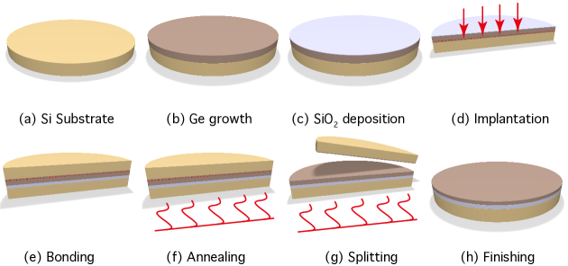
The process steps for the fabrication of germanium-on-insulator (GeOI) are schematically shown in Fig. SM1. At first, 2.5 m Ge is grown on 200 mm Si wafers via reduced-pressure chemical vapor deposition, followed by 200 nm SiO2 via plasma-enhanced chemical vapor deposition. Subsequently, a defect layer is locally created in the Ge layer by H+ ion implantation. Then, the wafer is bonded onto a silicon wafer which is covered with a thick thermal SiO2 layer. During the anneal of the bonded wafer stack, the pair splits at the defect layer created by ion implantation. Finally, the surface of the Ge layer is treated by chemical mechanical polishing.
II Modelling of carrier decay
From time-resolved synchrotron-based pump-probe transmission measurements, we extract the charge carrier density and fit the decay with a simple model including a non-radiative decay time and a decay time related to Auger processes. The decay of the charge carrier density is described by the equation
| (SM1) |
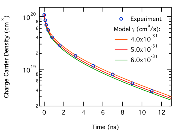
where is expressed with the Auger recombination coefficient as = 1/. After solving equation (1) for and fitting the model to the experimental data, we obtain the non-radiative recombination time and the Auger coefficient as 5.0 ns and 5.010-31 cm6/s, respectively. The robustness of the fit towards changes in is shown in Fig. SM2, where the decay model is plotted for three different Auger coefficients , revealing that the coefficient can be determined with an accuracy of 1.010-31 cm6/s.
III Estimation of carrier diffusion into constriction center
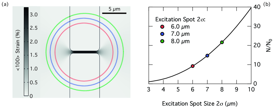
For temperature-dependent photoluminescence measurements, it is found that the luminescence increases for all structures upon cooling, although the calculated carrier population at the direct valley for the samples with indirect band gap (strain at 300 K smaller than approx. 3%, c.f. Fig. 3(b) in main text) decreases. We attribute this to the fact that the model does not take into account the diffusion of carriers from regions in close vicinity of the highly strained constriction into the center of the structure, which was previously shown to contribute to the intensity of the emission at maximum strain [SM1]. The same carrier collection effect has been acknowledged by Nam et al. from exploring so-called strain-induced pseudo-heterostructure nanowires [SM2].
For the here investigated structures, the area with a homogeneous distribution at maximum strain level is limited to 4.5 m 500 nm (c.f. finite element COMSOL modelling shown in Fig. SM3(a)). The excitation spot, however, extends over a larger area and is estimated to a width of 2 7 m which means that most of the carriers are excited outside of the region with the maximum strain. This is shown in Fig. SM3(b) where the area of excitation weighted with a 2-dimensional symmetric Gaussian distribution is compared to the area of the homogeneously strained part of the constriction. Depending on the collection efficiency, which itself depends on the temperature due to the increase in mobility, additional carriers will flow into the central region of the bridge where they recombine and thus enhance the PL efficiency, as is observed in the experiment.
IV Strain Conversion from Raman Shift
Commonly, strain is converted with a linear relation from Raman-shifts. For the case of uniaxial stress along 100, the strain is related to the Raman shift as
| (SM2) |
However, recent experiments correlating Raman spectroscopy with strain via Laue microdiffraction show that for high uniaxial stress, there is a deviation from the linear relation [SM3].
As a comparison, the strain values of the investigated structures at 300 K and 20 K are given in table SMI for both, the linear and the non-linear conversion.
| 100 Raman | (%) | (%) | (%) | (%) |
|---|---|---|---|---|
| 300 K | non-linear | linear | non-linear | linear |
| conversion | conversion | conversion | conversion | |
| -3.3 | 1.9 | 2.1 | 2.8 | 3.2 |
| -4.1 | 2.3 | 2.6 | 3.4 | 3.9 |
| -4.9 | 2.7 | 3.2 | 4.0 | 4.7 |
| -5.6 | 3.1 | 3.6 | 4.5 | 5.4 |
| -6.7 | 3.6 | 4.3 | 5.4 | 6.4 |
| M. J. Süess, R. Geiger, R. A. Minamisawa, G. Schiefler, J. Frigerio, D. Chrastina, G. Isella, R. Spolenak, J. Faist, and H. Sigg, Nature Photonics 7, 466 (2013). | |
| D. Nam, D. S. Sukhdeo, J.-H. Kang, J. Petykiewicz, J. H. Lee, W. S. Jung, J. Vuckovic, M. L. Brongersma, and K. C. Saraswat, Nano Letters 13, 3118 (2013). | |
| A. Gassenq, S. Tardif, K. Guilloy, I. Duchemin, G. Osvaldo Dias, N. Pauc, D. Rouchon, J.-M. Hartmann, J. Widiez, J. Escalante, Y.-M. Niquet, R. Geiger, T. Zabel, H. Sigg, J. Faist, A. Chelnokov, F. Rieutord, V. Reboud, and V. Calvo, submitted. |