Exponential Protection of Zero Modes in Majorana Islands
Majorana zero modes are quasiparticle excitations in condensed matter systems that have been proposed as building blocks of fault-tolerant quantum computers Kitaev:2003jw . They are expected to exhibit non-Abelian particle statistics, in contrast to the usual statistics of fermions and bosons, enabling quantum operations to be performed by braiding isolated modes around one another Kitaev:2003jw ; Nayak:2008dp . Quantum braiding operations are topologically protected insofar as these modes are pinned near zero energy, and the pinning is predicted to be exponential as the modes become spatially separated Read:392241 ; Kitaev:2001kla . Following theoretical proposals Lutchyn:2010hpa ; Oreg:2010gk , several experiments have identified signatures of Majorana modes in proximitized nanowires Mourik:2012je ; Rokhinson:2012ep ; Das:2012hi ; Deng:2012gn ; Churchill:2013cq and atomic chains NadjPerge:2014ey , with small mode-splitting potentially explained by hybridization of Majoranas DasSarma:2012kt ; Stanescu:2013je ; Rainis:2013zxa . Here, we use Coulomb-blockade spectroscopy in an InAs nanowire segment with epitaxial aluminum, which forms a proximity-induced superconducting Coulomb island (a Majorana island ) that is isolated from normal-metal leads by tunnel barriers, to measure the splitting of near-zero-energy Majorana modes. We observe exponential suppression of energy splitting with increasing wire length. For short devices of a few hundred nanometers, sub-gap state energies oscillate as the magnetic field is varied, as is expected for hybridized Majorana modes. Splitting decreases by a factor of about ten for each half a micrometer of increased wire length. For devices longer than about one micrometer, transport in strong magnetic fields occurs through a zero-energy state that is energetically isolated from a continuum, yielding uniformly spaced Coulomb-blockade conductance peaks, consistent with teleportation via Majorana modesFu:2010ho ; Hutzen:2012gg . Our results help to explain the trivial-to-topological transition in finite systems and to quantify the scaling of topological protection with end-mode separation.
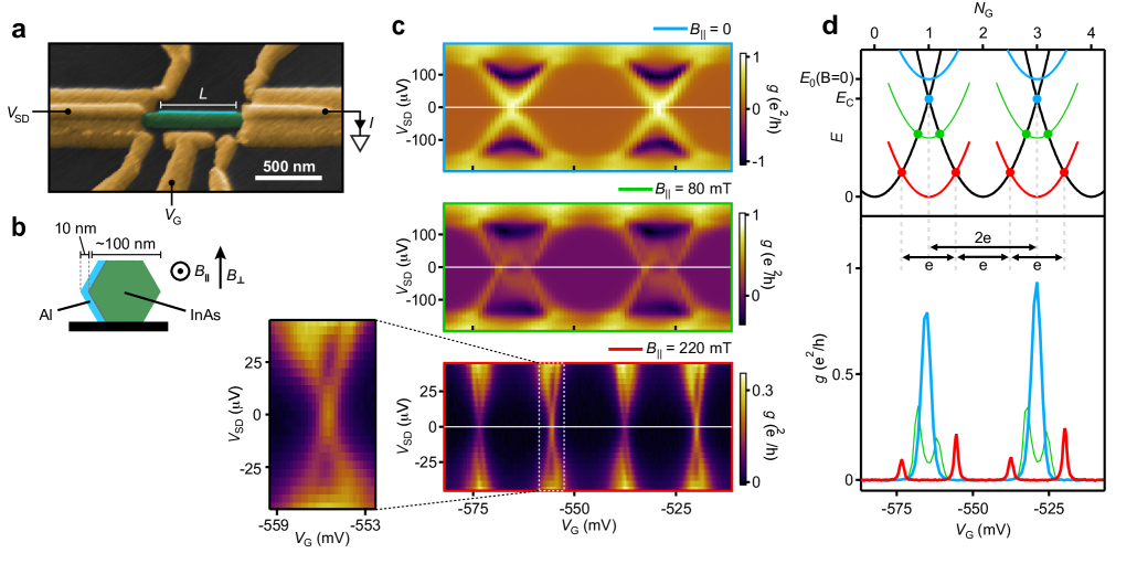
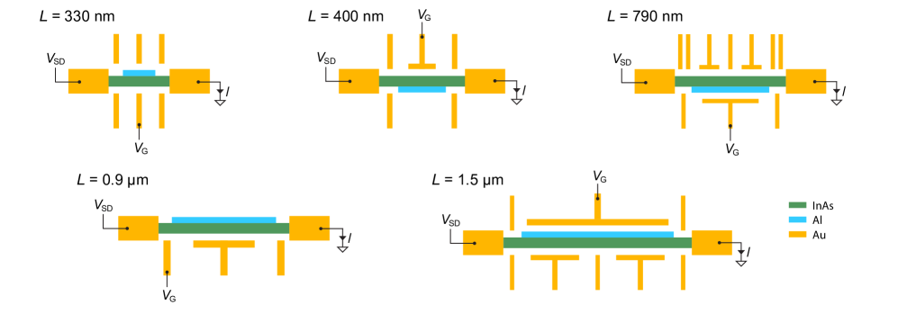
The set of structures we investigate consist of InAs nanowires grown by molecular beam epitaxy in the wurtzite direction with an epitaxial Al shell on two facets of the hexagonal cross section 2015NatMa..14..400K . The Al shell was removed except in a small segment of length and isolated from normal metal (Ti/Au) leads by electrostatic gate-controlled barriers (Fig. 1a). Charging energy, , of the device ranges from greater than to less than the superconducting gap of Al ( 0.2 meV). The thin Al shell ( thickness on the two facets) gives a large critical field, , before superconductivity is destroyed: for fields along the wire axis, ; out of the plane of the substrate but roughly in the plane of the two Al-covered facets, (Fig. 1b). The very high achieved critical fields make these wires a suitable platform for investigating topological superconductivity 2015NatMa..14..400K .
Five devices over a range of Al shell lengths m were measured (see Methods for device layouts). Charge occupation and tunnel coupling to the leads were tuned via electrostatic gates. Differential conductance, , in the Coulomb blockade regime (high-resistance barriers) was measured using standard ac lock-in techniques in a dilution refrigerator (electron temperature ).
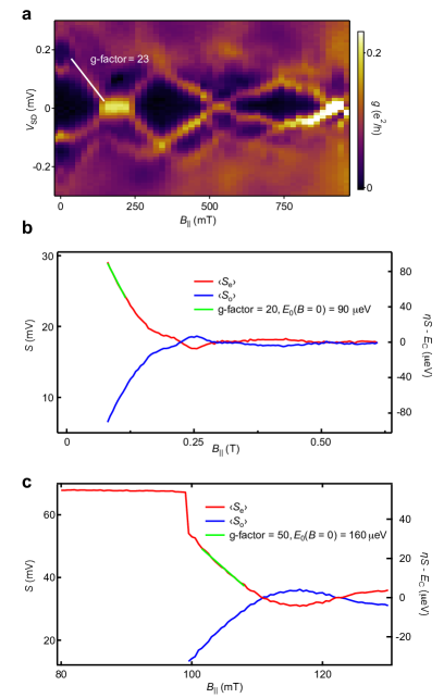
Figure 1c shows as a function of gate voltage, , and source-drain bias, . For the device, the zero-field data (top panel) show a series of evenly spaced Coulomb diamonds with a characteristic negative-differential conductance (NDC) region at higher bias. NDC is known from metallic superconductor islands Hekking:1993gc ; Hergenrother:1994ei and has recently been reported in a proximitized semiconductor device similar to those investigated here Higginbotham:2015wc . The zero-magnetic-field diamonds reflect transport via Cooper pairs, with gate voltage period proportional to , the charge of a Cooper pair. At moderate magnetic fields (Fig. 1c, middle panel), the large diamonds shrink and a second set of diamonds appears, yielding even-odd spacing of Coulomb blockade zero-bias conductance peaks Eiles:1993uh , as seen in the cuts in Fig. 1d. At larger magnetic fields (Fig. 1c, lower panel) Coulomb diamonds are again periodic, now with precisely half the spacing of the zero-field diamonds, corresponding to periodicity. NDC is absent, and resonant structure is visible within each diamond, indicating transport through discrete resonances at low bias and a continuum at high bias (see magnification in Fig. 1c). Coulomb blockade conductance peaks at high magnetic field (see Fig. 1d for zero bias cuts) with regular periodicity (half the zero-field spacing) accompanied by a discrete subgap spectrum is a proposed signature of electron teleportation by Majorana end states Fu:2010ho ; Hutzen:2012gg . We designate as a ‘Majorana island’ (MI) the ungrounded tunneling device in this high-field regime, where a subgap state near zero energy, energetically isolated from a continuum, leads to 1-periodic Coulomb blockade conductance peaks.
Zero-bias conductance can be qualitatively understood within a simple zero-temperature model where the energy of the superconducting island—with or without subgap states (Fig. 1d)—is given by a series of shifted parabolas, , where is the gate-induced charge (electron charge and gate capacitance ) Tuominen:1992vy ; Eiles:1993uh ; Hekking:1993gc ; Lafarge:1993zz ; Hergenrother:1994ei ; 1994MPLB….8.1007M . is the energy of the lowest quasiparticle state, which is filled for odd parity (, odd ), and empty for even parity (, even ) Higginbotham:2015wc . Transport occurs when the ground state has a charge degeneracy, i.e., when the parabolas intersect. For , the ground state always has even parity; transport in this regime occurs via tunneling of Cooper pairs at degeneracies of the even- parabolas. This is the regime of the -periodic Coulomb blockade peaks seen at low magnetic fields (Fig. 1d, blue). The odd charge state is spinful and can be lowered by Zeeman energy when a magnetic field is applied. For sufficiently large field, such that , an odd- ground state emerges. This transition from 2 charging to 1 charging is seen experimentally as the splitting of the -periodic Coulomb diamonds into the even-odd double-diamond pattern in Fig. 1d (green trace). In this regime the Coulomb peak spacing is proportional to for even diamonds and for odd diamonds Tuominen:1992vy ; Lafarge:1993zz . For the particular case of a zero-energy Majorana state, , peak spacing is regular and -periodic. This regime is observed at higher fields (Fig. 1d, red), though not sufficiently high to destroy superconductivity.
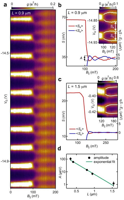
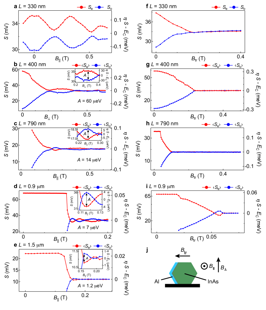
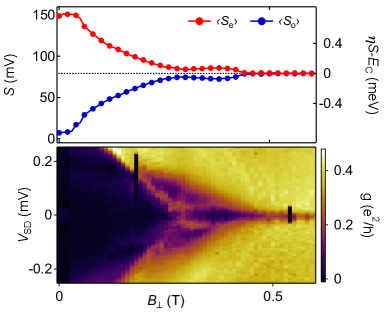
Coulomb peak spacings are measured as a function of magnetic field, allowing the state energy, , to be extracted. An example, showing 10 consecutive peaks for the device, is shown in Fig. 2a. The peaks are -periodic at , start splitting around , and become -periodic at , well below the spectroscopically observed closing of the superconducting gap at (see Methods). This points towards the presence of a state close to zero energy within the superconducting regime over a range of .
Separately averaging even and odd Coulomb peak spacings, , over an ensemble of adjacent peaks reveals oscillations around the -periodic value as a function of applied magnetic field. This is consistent with an oscillating state energy due to hybridized Majorana modes Rainis:2013zxa ; DasSarma:2012kt ; Stanescu:2013je . For the device (Fig. 2b), peak spacing oscillations yield an energy oscillation amplitude , converted from gate voltage to energy using the gate lever arm, , extracted independently from the slope of the Coulomb diamonds. For the device (Fig. 2c) average Coulomb peak spacing oscillations based on 22 consecutive peaks yield a barely resolvable amplitude, .
Oscillation amplitudes for the five measured devices (see Methods for device details), are shown in Fig. 2d along with a two-parameter fit to an exponential function, , giving and as fit parameters. The data fits well to the predicted exponential form that characterizes the topological protection of Majorana modes Read:392241 ; Kitaev:2001kla ; DasSarma:2012kt .
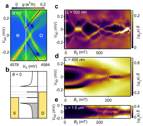
Excited states of the MI are probed using finite-bias transport spectroscopy. This technique requires a fixed gate voltage, chosen such that at zero bias the electrochemical potential of the leads aligns with the middle of the spectroscopic gap of the MI. With this choice, the conductance at source-drain bias is due to states at energy . A conductance peak at zero bias corresponds to a zero-energy state. In the case shown in Figs. 3(a,b), the gate voltage is tuned using the characteristic finite-bias conductance spectra for a short InAs/Al island, investigated previously in Ref. Higginbotham:2015wc . Ground-state energies determined by finite-bias spectroscopy match those extracted from zero-bias peak spacings (see Methods Fig. S7).
Bias spectroscopy shows discrete zero-energy states emerging at sufficient applied field over a range of device lengths. In a short device (Fig. 3c), the discrete state moves linearly in magnetic field, passing through zero and merging with a continuum at . This merging is expected for Majorana systems in the short-length limit, where quenching of spin-orbit coupling results in unprotected parity crossings and state intersections at high energy Stanescu:2013je . Rather than passing directly through zero, the first zero crossing extends for , which is not understood. Medium-length devices show the subgap state bending back toward zero after zero crossings (Fig. 3d), in agreement with theoretical predictions for the emergence of Majorana behavior with increasing system length Stanescu:2013je ; Rainis:2013zxa . For a long device (m), bias spectroscopy shows a zero-energy state separated from a continuum at higher bias (Fig. 3e). The zero-energy state is present over a field range of , with an associated energy gap .
The evolution from unprotected parity crossings, to energetically isolated oscillating states, and then to a fixed zero-energy state, with increasing device length is consistent with the expected crossover from a strongly overlapping precursor of split Majoranas to a topologically protected Majorana state locked at zero energy Stanescu:2013je ; Rainis:2013zxa . Note that in the data in Fig. 3e, the signal from the discrete state disappears above . This is not expected within a simple Majorana picture. Even though the zero-bias peak disappears, the peak spacing remains -periodic (see Methods).
The observed effective g-factors, , extracted from the addition spectrum and bias spectroscopy (see Methods), are large compared to previous studies on InAs nanowires Csonka:2008gz ; Schroer:2011ev ; Das:2012hi , perhaps resulting from field focusing from the Al shell. The measured gap to the continuum at zero magnetic field is consistent with the gap of aluminum , and is roughly the same in all devices. The discrete subgap states (Fig. 3c-e) have zero-field energy less than but comparable to the gap, ranging from , consistent with expectations for half-shell geometries Cole:2015vf . The measured gap between the near-zero-energy state and the continuum in the high-field (topological) regime, , along with the coherence length extracted from the exponential fit to the length-dependent splitting (Fig. 2d), , are consistent with topological superconductivity. Within this picture, at low magnetic fields, the gap and coherence length are related to the strength of spin-orbit coupling, yielding a value that is consistent with previously reported values in InAs nanowires Fasth:2007ie ; Das:2012hi . For a single subband picture, this implies a Fermi velocity that is lower than expected, suggesting that more than one subband is occupied under the Al shell, though we are not able to extract the number of modes directly.
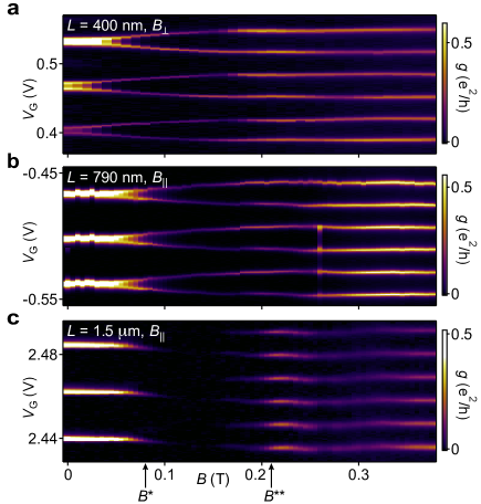
Finally, we consider the magnetic field dependence of Coulomb blockade peak heights (as opposed to spacings), as seen in Fig. 4. We found in most devices that below the field where -periodic peaks split, all peaks were uniformly high amplitude. Above , peak heights were rapidly suppressed and remained low up to a second characteristic field, , coincident with periodicity (i.e., the field where even-odd spacing differences vanished). Above , peak heights recovered. In the longer wires, peaks were nearly absent between and , as seen in Fig. 4c.
We interpret these observations as follows: In the present lead-wire-lead geometry, transport above involves single electrons entering one end of the wire and leaving from the other. The onset of uniform spacing with the reappearance of high peaks above indicates the emergence of a state (or states) at zero energy with strong wave function support at both ends of the wire. This is consistent with teleportation of electrons from one end of the wire to the other via a Majorana mode Fu:2010ho ; Hutzen:2012gg , though not necessarily a unique signature 2015PhRvB..92b0511S . Thus while the simultaneous brightening of peaks with their becoming uniformly spaced at suggests a subgap/Majorana mode moving to the ends of the wire as it moves to zero energy, we cannot rule out other forms of end-localized zero-energy states that could appear above a critical field.
In summary, we have studied Majorana islands composed of InAs nanowires covered on two facets with epitaxial Al, for a range of device lengths. Zero-energy states are observed for wires of all lengths away from zero field. Oscillating energy splittings, measured using Coulomb blockade spectroscopy, are exponentially suppressed with wire length, with a characteristic length . This constitutes an explicit demonstration of exponential protection of zero-energy modes. Finite-bias measurements show transport through a discrete zero-energy state, with a measured topological gap for long devices. The extracted and are consistent with known parameters for InAs nanowires and the emergence of topological superconductivity. Brightening of Coulomb peaks at the field where spacing becomes uniform for longer devices suggests the presence of a robust delocalized state connecting the leads, and provides experimental support for electron teleportation via Majorana modes.
Acknowledgements
We thank K. Flensberg, M. Leijnse, M. Deng, W. Chang, and R. Lutchyn for valuable discussions, and G. Ungaretti, S. Upadhyay, C. Sørensen, M. von Soosten, and D. Sherman for contributions to growth and fabrication. Research supported by Microsoft Project Q, the Danish National Research Foundation, the Lundbeck Foundation, the Carlsberg Foundation, and the European Commission. CMM acknowledges support from the Villum Foundation.
Author contributions
P.K., T.S.J. and J.N. developed the nanowire materials. S.M.A. fabricated the devices. S.M.A., A.P.H. and M.M. carried out the measurements with input from F.K., T.S.J. and C.M.M. Data analysis was done by S.M.A., A.P.H. and M.M. All authors contributed to interpreting the data. The manuscript was written by S.M.A., A.P.H. and C.M.M. with suggestions from all other authors.
References
- (1) Kitaev, A. Y. Fault-tolerant quantum computation by anyons. Annals of Physics 303, 2–30 (2003).
- (2) Nayak, C., Simon, S. H., Stern, A., Freedman, M. & Das Sarma, S. Non-Abelian anyons and topological quantum computation. Reviews of Modern Physics 80, 1083–1159 (2008).
- (3) Read, N. & Green, D. Paired states of fermions in two dimensions with breaking of parity and time-reversal symmetries, and the fractional quantum Hall effect. Physical Review B 61, 10267 (2000).
- (4) Kitaev, A. Y. Unpaired Majorana fermions in quantum wires. Phys.Usp. 44, 131–136 (2001).
- (5) Lutchyn, R. M., Sau, J. D. & Das Sarma, S. Majorana Fermions and a Topological Phase Transition in Semiconductor-Superconductor Heterostructures. Physical Review Letters 105, 077001 (2010).
- (6) Oreg, Y., Refael, G. & von Oppen, F. Helical Liquids and Majorana Bound States in Quantum Wires. Physical Review Letters 105, 177002 (2010).
- (7) Mourik, V. et al. Signatures of Majorana Fermions in Hybrid Superconductor-Semiconductor Nanowire Devices. Science 336, 1003–1007 (2012).
- (8) Rokhinson, L. P., Liu, X. & Furdyna, J. K. The fractional a.c. Josephson effect in a semiconductor-superconductor nanowire as a signature of Majorana particles. Nature Physics 8, 795–799 (2012).
- (9) Das, A. et al. Zero-bias peaks and splitting in an Al-InAs nanowire topological superconductor as a signature of Majorana fermions. Nature Physics 8, 887–895 (2012).
- (10) Deng, M. T. et al. Anomalous Zero-Bias Conductance Peak in a Nb–InSb Nanowire–Nb Hybrid Device. Nano Letters 12, 6414–6419 (2012).
- (11) Churchill, H. O. H. et al. Superconductor-nanowire devices from tunneling to the multichannel regime: Zero-bias oscillations and magnetoconductance crossover. Physical Review B 87, 241401 (2013).
- (12) Nadj-Perge, S. et al. Observation of Majorana fermions in ferromagnetic atomic chains on a superconductor. Science 346, 602–607 (2014).
- (13) Das Sarma, S., Sau, J. D. & Stanescu, T. D. Splitting of the zero-bias conductance peak as smoking gun evidence for the existence of the Majorana mode in a superconductor-semiconductor nanowire. Physical Review B 86, 220506 (2012).
- (14) Stanescu, T. D., Lutchyn, R. M. & Das Sarma, S. Dimensional crossover in spin-orbit-coupled semiconductor nanowires with induced superconducting pairing. Physical Review B 87, 094518 (2013).
- (15) Rainis, D., Trifunovic, L., Klinovaja, J. & Loss, D. Towards a realistic transport modeling in a superconducting nanowire with Majorana fermions. Physical Review B 87, 024515 (2013).
- (16) Fu, L. Electron Teleportation via Majorana Bound States in a Mesoscopic Superconductor. Physical Review Letters 104, 056402 (2010).
- (17) Hützen, R., Zazunov, A., Braunecker, B., Yeyati, A. L. & Egger, R. Majorana Single-Charge Transistor. Physical Review Letters 109, 166403 (2012).
- (18) Krogstrup, P. et al. Epitaxy of semiconductor-superconductor nanowires. Nature Materials 14, 400–406 (2015).
- (19) Hekking, F., Glazman, L., Matveev, K. & Shekhter, R. Coulomb blockade of two-electron tunneling. Physical Review Letters 70, 4138–4141 (1993).
- (20) Hergenrother, J., Tuominen, M. & Tinkham, M. Charge transport by Andreev reflection through a mesoscopic superconducting island. Physical Review Letters 72, 1742–1745 (1994).
- (21) Higginbotham, A. P. et al. Parity lifetime of bound states in a proximitized semiconductor nanowire. Nature Physics 11, 1017–1021 (2015).
- (22) Eiles, T. M., Martinis, J. M. & Devoret, M. H. Even-odd asymmetry of a superconductor revealed by the Coulomb blockade of Andreev reflection. Physical Review Letters 70, 1862–1865 (1993).
- (23) Tuominen, M. T., Hergenrother, J. M., Tighe, T. S. & Tinkham, M. Experimental evidence for parity-based 2 periodicity in a superconducting single-electron tunneling transistor. Physical Review Letters 69, 1997–2000 (1992).
- (24) Lafarge, P., Joyez, P., Esteve, D., Urbina, C. & Devoret, M. H. Measurement of the even-odd free-energy difference of an isolated superconductor. Physical Review Letters 70, 994–997 (1993).
- (25) Matveev, K. A., Glazman, L. I. & Shekhter, R. I. Effects of Charge Parity in Tunneling Through a Superconducting Grain. Modern Physics Letters B 8, 1007–1026 (1994).
- (26) Csonka, S., Hofstetter, L., Freitag, F. & Oberholzer, S. Giant fluctuations and gate control of the g-factor in InAs nanowire quantum dots. Nano Letters 8, 3932–3935 (2008).
- (27) Schroer, M. D., Petersson, K. D., Jung, M. & Petta, J. R. Field Tuning the g Factor in InAs Nanowire Double Quantum Dots. Physical Review Letters 107, 176811 (2011).
- (28) Cole, W. S., Das Sarma, S. & Stanescu, T. D. Effects of large induced superconducting gap on semiconductor Majorana nanowires. Physical Review B 92, 174511 (2015).
- (29) Fasth, C., Fuhrer, A., Samuelson, L., Golovach, V. N. & Loss, D. Direct Measurement of the Spin-Orbit Interaction in a Two-Electron InAs Nanowire Quantum Dot. Physical Review Letters 98, 266801 (2007).
- (30) Sau, J. D., Swingle, B. & Tewari, S. Proposal to probe quantum nonlocality of Majorana fermions in tunneling experiments. Physical Review B 92, 020511 (2015).
I Methods
I.1 Sample preparation
The InAs nanowires with epitaxial Al shell were grown via a two-step process by molecular beam epitaxy. First, the InAs nanowires were grown using the vapor-liquid-solid method with Au as a catalyst at C. Second, after cooling the system to C the Al was grown on two facets of the hexagonal cross section 2015NatMa..14..400K . Afterwards the nanowires were deposited on degenerately doped Si substrates with 100-500 nm thick thermal oxides using either wet or dry deposition techniques. Wet deposition involves sonicating a growth substrate of nanowires in methanol for a few seconds, then putting several drops of the nanowire-methanol solution onto the chip surface using a pipette. Dry deposition was done by bringing a small piece of cleanroom wipe in touch with the growth substrate, then afterwards swiping it onto the chip surface. We find that while wet deposition results in a more uniform dispersion of nanowires on the chip surface, dry deposition is faster and less wasteful with nanowires. Selective removal of the Al shell was done by patterning etch windows using electron beam lithography on both sides of the nanowire, plasma cleaning the surface of the nanowire using oxygen, then etching the Al using a Transene Al Etchant D with an etching time of 10 seconds at C. Depending on the device, ohmic contacts to the InAs core were fabricated using either ion milling or sulfur passivation to remove surface oxides. Ion milling was done for times ranging from 85 s to 110 s using a Kaufman & Robinson KDC 40 4-CM DC Ion Source with an acceleration voltage of 120V and an ion beam current density of 0.5 mA/ at the chip surface. Sulfur passivation was done using a 2.1% solution of in DI water with 0.15 M dissolved elemental sulfur at C for 20 minutes. This was followed by the deposition of of Ti as a sticking layer and of Au for the ohmic contact. We found that ion milling resulted in more stable devices. Side and plunger gates were lithographically defined in the same fabrication step as the ohmic contacts in order to increase device yield. PMMA was used as resist in all lithography steps.
I.2 Device Geometries
Gate patterns of the five measured devices are shown in ED Fig. 1. With the exception of the device, all measurements involving gate dependence are tuned through resonances using the plunger gate on either the Al side or the uncoated InAs side. For the device, the lower left side gate is used to tune through resonances of the quantum dot, because the central plunger gate was not bonded during the cool down.
I.3 Measurements
Transport measurements were carried out in an Oxford Triton dilution refrigerator with a base electron temperature of and a 6-1-1 T vector magnet. Differential conductance, , was measured using the AC-lockin technique with an excitation voltage in the range 2-6 .
I.4 Peak spacing data summary
The exponential curve in Fig. 2d (main text) is derived from even-odd peak spacing measurements in the high critical field directions, and , summarized in ED Fig. 2. Suppression of spacing fluctuations with increased device length is clearly visible. The measured is indicated by black arrows in the inset, and the values are recorded in ED Table 1 for each device length, along with charging energies and lever arms.
For , Coulomb peak fluctuations became uncorrelated after several peaks. To obtain a large statistical ensemble, fluctuations were averaged over five sets of Coulomb peaks taken in different device tunings. ED Fig. 2a shows data from a single set of peaks, and ED Table 1 reports the full ensemble average.
In a transverse magnetic field applied in the low critical field direction, , shown in ED Fig. 2f-i, the oscillations are absent, with the exception of an initial overshoot for at (ED Fig. 2i), before the system is driven into the normal state at .
| L [] | [] | [] | [] |
|---|---|---|---|
| 330 | 1.6 | 0.048 | 106 |
| 400 | 0.40 | 0.012 | 60 |
| 790 | 0.14 | 0.008 | 14 |
| 950 | 0.054 | 0.0016 | 7 |
| 1540 | 0.022 | 0.002 | 1.2 |
I.5 Magnetic Field Orientation
The direction of the nanowire on the chip was found by orienting the magnetic field from a vector magnet in the chip plane and spectroscopically measuring the anisotropy of the critical magnetic field. By comparing to the wire-direction based on optical and electron micrographs, we estimate an angular precision of degrees.
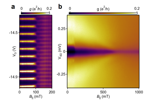
I.6 Critical Field Measurements
The observed - splitting at is compared to the closing of the superconducting gap at a considerably higher critical field, , in ED Fig. 3. Bias spectroscopy in ED Fig. 3b shows a closing of the superconducting gap at , more than 500 mT after the onset of evenly spaced -periodic Coulomb peaks. The change from to -periodicity at in ED Fig. 3a coincides with a reduction in the measured Coulomb gap in ED Fig. 3b, reflecting the transition from Cooper pair charging (energy penalty ) to single-electron charging (energy penalty ). The measurement in ED Fig. 3b was taken in a Coulomb valley at the gate voltage .
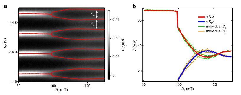
I.7 Averaging of peak spacings
In Fig. 2b of the main text, we show the extracted average peak spacing for several even and odd Coulomb valleys. A high resolution measurement of the - splitting is shown in ED Fig. 4a. The individual even and odd valleys, in ED Fig. 4b, exhibit the same oscillating behavior but show a small deviation from the average between , which might be attributable to -factor fluctuations for successive charge occupations of the quantum dot. Below 100 mT the fluctuations are very small, giving an indication of instrumental noise in the measurement.
I.8 Angle Dependence
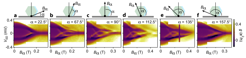
Angle dependence of the anti-crossing of the state with the continuum for is shown in ED Fig. 5. We focus on magnetic fields, , with angles, , in the plane perpendicular to the nanowire direction. The measurements show a pronounced anti-crossing between the sub-gap state and an excitation continuum ( and ) that is significantly reduced for . Interpreting angle dependence is complicated by the anisotropy of g-factor and critical field. The critical field is maximized for , and is reduced drastically for near-perpendicular field alignment (). The observed g-factors are highly dependent on field orientation and device tuning. For the device shown in ED Fig. 5, we found an approximately sinusoidal variation in -factor by a factor of 2, with maximum g-factor occurring near .
I.9 Choice of gate voltage for bias spectroscopy

For bias spectroscopy, the gate voltage is fixed either by interpreting Coulomb diamonds, as discussed in the main text, or from even-odd peak spacings. While details of the bias spectroscopy, such as locations of zero-crossing, depend on the choice of gate voltage, general features such as slopes, typical fluctuation amplitude, and the presence of a robust excitation gap are not strongly affected by the choice of gate voltage (ED Fig. 6).
I.10 Comparison of addition energies and finite bias spectroscopy
Peak spacings are used to measure the energy of the lowest-lying state. The same information is present in the bias spectroscopy, and gives consistent results, as shown in ED Fig. 7.
I.11 Bias spectroscopy of long device
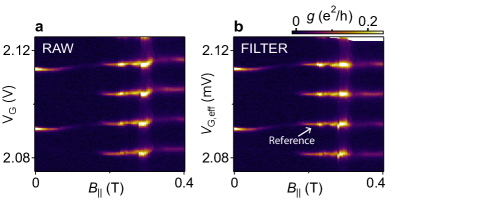
Common-mode fluctuations in Coulomb peak position were observed in the longest () device, as shown in ED Fig. 8a. The fluctuations evidently correspond to a shift in the electrochemical potential of the dot, likely due to a nearby, field-dependent charge trap. The fluctuations are small compared to charging energy, but complicate the application of bias spectroscopy which needs to be performed at fixed electrochemical potential. To correct for the fluctuations, we introduce an effective gate voltage,
| (1) |
that removes the common-mode peak motion. The offset voltage is zero at low field, when Coulomb peaks are periodic ( for ). At high field, is chosen so that the reference Coulomb peak (labeled in ED Fig. 8b) occurs at constant . All nonzero are listed in ED Table 2.
| B (mT) | |
|---|---|
| 180 | 0.25 |
| 230 | 0.25 |
| 235 | 0.25 |
| 240 | 0.25 |
| 245 | 0.25 |
| 250 | 0.25 |
| 255 | 0.25 |
| 260 | 0.5 |
| 265 | 0.5 |
| 270 | 0.5 |
| 275 | 0.5 |
| 280 | 0.75 |
| 300 | 0.25 |
| 305 | 0.75 |
| 310 | 1.25 |
| 315 | 1.5 |
| 320 | 1.75 |
| 325 | 1.75 |
| 330 | 1.75 |
| 335 | 1.75 |
| 340 | 1.75 |
| 345 | 1.75 |
| 350 | 1.75 |
| 355 | 1.75 |
| 360 | 1.75 |
| 365 | 1.75 |
| 370 | 1.75 |
| 375 | 1.75 |
| 380 | 1.75 |
| 385 | 1.75 |
| 390 | 1.75 |
| 395 | 1.75 |
| 400 | 1.75 |
As shown in ED Fig. 8b, this procedure removes the common-mode peak motion. In the case of the device, bias spectroscopy is performed at fixed , which allows us to infer the energy of the sub-gap state at fixed electrochemical potential.
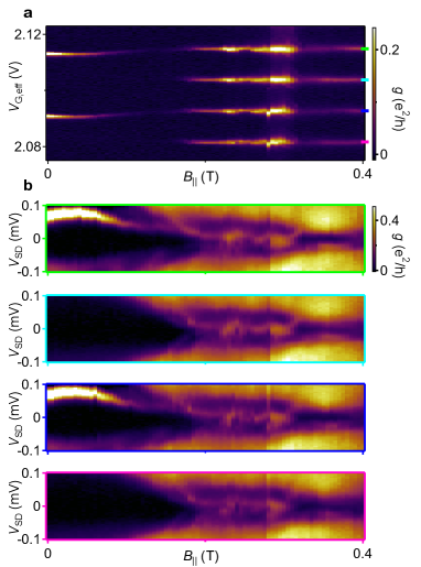
I.12 Zero-energy state at successive Coulomb peaks
The zero-energy state is robust over many successive Coulomb peaks, as shown in ED Fig. 9. The full bias spectroscopy as a function of field is also reproducible over several peaks, as shown in ED Fig. 10.

I.13 Measured g-factors
As can be seen in ED Fig. 11 the state energy does not move linearly in magnetic field. A non-linear behavior with magnetic field is expected in the presence of strong spin-orbit coupling and a finite critical field.
If the behavior was strictly linear one would expect
| (2) |
because the peak splitting at occurs when and the state is at zero energy at when (see Fig. 4 in the main text for reference). The non-linear behavior of at higher magnetic fields approaching renders this unsuitable for an accurate measurement of the state energy at zero field.
In the low field regime where the state energy is approximately linear with magnetic field we calculate an effective g-factor. Using this slope it is possible to give a rough estimate of the state energy assuming linear behavior and extrapolating the state energy to zero magnetic field.
For bias spectroscopy it should be noted that for gate voltages in the middle of the spectroscopic gap (see main text) transport through a state at indicates a state energy . An example for is shown in ED Fig. 11a.
Using the addition spectrum, the state energy can be calculated from the peak spacing according to . Examples of extracted effective g-factors in the linear range are shown in ED Fig. 11b,c.