Quantization of Hall Resistance at the Metallic Interface between an Oxide Insulator and SrTiO3
Abstract
The two-dimensional metal forming at the interface between an oxide insulator and SrTiO3 provides new opportunities for oxide electronics. However, the quantum Hall effect, one of the most fascinating effects of electrons confined in two dimensions, remains underexplored at these complex oxide heterointerfaces. Here, we report the experimental observation of quantized Hall resistance in a SrTiO3 heterointerface based on the modulation-doped amorphous-LaAlO3/SrTiO3 heterostructure, which exhibits both high electron mobility exceeding 10,000 cm2/V s and low carrier density on the order of 1012 cm-2. Along with unambiguous Shubnikov–de Haas oscillations, the spacing of the quantized Hall resistance suggests that the interface is comprised of a single quantum well with ten parallel conducting two-dimensional sub-bands. This provides new insight into the electronic structure of conducting oxide interfaces and represents an important step towards designing and understanding advanced oxide devices.
The quantum Hall effect (QHE), arises from quantization of the cyclotron motion of charge carriers subjected to a perpendicular magnetic field. The cyclotron motion becomes quantized when electrons complete enclosed orbits without being scattered, and the observation of the QHE therefore requires materials with high carrier mobility. Consequently, it has only been observed in a few material systems such as semiconductor heterostructures based on silicon Klitzing et al. (1980) or III-V compounds Tsui et al. (1982), Bi2Se3 Cao et al. (2012) and graphene Zhang et al. (2005). Recent technical advances in the growth of oxides have resulted in the creation of high-mobility two-dimensional electron gases (2-DEGs) at heterointerfaces based on either ZnO Tsukazaki et al. (2007, 2010) or SrTiO3 (STO) Ohtomo and Hwang (2004); Chen et al. (2013). Remarkably, the mobility enhancement made in polar MgZnO/ZnO heterostructures has led to the observation of both integer and fractional QHE Tsukazaki et al. (2007, 2010); Falson et al. (2015). The conducting states of ZnO-based heterostructures are, however, similar to the conventional semiconductor heterostructures, derived from sp hybrid orbitals with a covalent bond nature. In contrast, the interface conductivity in STO-based heterostructures originates from less overlapping Ti 3d orbitals, where the resulting ionic bonds lead to a strong coupling between the lattice, charge and spin degrees of freedom. The strong electronic correlations give rise to a variety of properties, such as gate-tunable superconductivity, magnetism, and tunable metal-insulator transitions Thiel et al. (2006); Christensen et al. (2013); Reyren et al. (2007); Caviglia et al. (2008); Brinkman et al. (2007), which has generated particular interest in STO-based heterostructures Sulpizio et al. (2014).
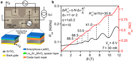
The metallic conductivity of STO-based heterostructures originates from degenerate Ti 3d t2g levels Delugas et al. (2011); Son et al. (2009); Khalsa and MacDonald (2012); Breitschaft et al. (2010) with the orbital occupation strongly depending on the carrier density. Below a threshold carrier density of 1.71013 cm-2 in the intensively investigated LaAlO3/SrTiO3 (LAO/STO) interface Joshua et al. (2012), electrons are confined within a thin sheet of STO in Ti 3dxy levels that are characterized by strong coupling parallel to the interface. Above this threshold density, electrons begin to populate the 3dxz/yz levels, which extend further away from the interface and add out-of-plane coupling to the electronic system Gabay and Triscone (2013). The Fermi surfaces of STO-based heterointerfaces have been probed by Shubnikov–de Haas (SdH) oscillations in the longitudinal resistance, Rxx Chen et al. (2013); Caviglia et al. (2010a); Ben Shalom et al. (2010); Xie et al. (2014); McCollam et al. (2014); Son et al. (2010). Notably, the carrier density deduced from SdH oscillations, n, is often more than 1 order of magnitude lower than that obtained by the Hall effect, n. This discrepancy has been ascribed to the hypothesis that only a small fraction of the carriers contributes to the SdH oscillations Chen et al. (2013); Caviglia et al. (2010a); Ben Shalom et al. (2010); Xie et al. (2014); McCollam et al. (2014); Son et al. (2010). Although the two-dimensional nature of the interface conductivity is demonstrated by the dependence of the SdH oscillations on magnetic field tilt angle, only a few studies report plateaulike structures in the Hall resistance, Rxy Xie et al. (2014); McCollam et al. (2014). Full analysis of the quantizationlike Hall resistance in these studies was, however, difficult due to irregular SdH oscillation spectra Xie et al. (2014); McCollam et al. (2014). Consequently, a clear QHE with well-defined quantized Hall plateaus coinciding with SdH oscillation minima remains undemonstrated at complex oxide interfaces. Here, we report unambiguous experimental observation of quantized Hall resistance in complex oxides (see Fig. 1b). Remarkably, the inverse Hall resistance (R) is found to be regularly spaced for all plateaus following the relation R = , with h being Planck’s constant, e the electron charge, the filling factor step, N a scaling factor equaling 10, and . This manifestation of the QHE is different from what is usually observed in conventional semiconductors, MgZnO/ZnO or other two-dimensional materials Klitzing et al. (1980); Tsui et al. (1982); Cao et al. (2012); Zhang et al. (2005); Tsukazaki et al. (2007, 2010); Falson et al. (2015), highlighting the exotic nature and potential opportunities of complex oxide devices. As will become clear later, our results are consistent with the oxide interface being comprised of a single quantum well hosting ten parallel conducting Ti 3dxy sub-bands, which is in contrast to the usual situation in LAO/STO for n 1.71013 cm-2 where all t2g levels (Ti 3dxy and 3dxz/yz sub-bands) are occupied.
The modulation-doped oxide interface is realized by inserting a La7/8Sr1/8MnO3 (LSM) spacer layer at the interface between amorphous LAO (a-LAO) and the crystalline STO substrate (a-LAO/LSM/STO) Chen et al. (2015). A Hall bar device is fabricated (see Fig. 1a) by conventional electron-beam lithography and an oxide hard mask of a-LSM Trier et al. (2015) rather than a-LAO Schneider et al. (2006). Standard ac lock-in measurements (Iac = 10 nA, fac = 77.03 Hz) are performed in a dilution refrigerator at temperatures between 30 mK and 3 K, back gate potentials (Vg) between and 10 V, and magnetic fields between 0 and 12 T. Sample rotation between 0∘ and 82∘ is achieved by a piezoelectric rotator. SdH oscillations are fitted by the analytical expression from Coleridge et al. Coleridge et al. (1989). Density functional theory-based tight binding (DFT-TB) calculations follow the approach outlined by Zhong et al. Zhong et al. (2013).
The Hall bar device shows metallic conductivity similar to the unpatterned interface Chen et al. (2015) with a carrier density n = 1/(RH) 5.61012 cm-2, where RH = dRxy/dB is the Hall coefficient, and a Hall carrier mobility, = 1/(enRxx) 8,703 cm2/V s, at 2 K and Vg = 0 V. This mobility is among the highest reported values for patterned complex oxide interfaces, which is typically below 1000 cm2/V s at 2 K Schneider et al. (2006); Stornaiuolo et al. (2012). Importantly, such an enhanced mobility, along with a low carrier density, enables us to observe the quantization of Hall resistance. Note that Rxx(B) Rxx(B) and Rxy(B) Rxy(B) [Supplemental Material (SM) Fig. S1]: therefore, the subsequent measurements only concern positive magnetic field direction. In order to examine the Fermi surface of the system based on our initial observation of the SdH oscillations Chen et al. (2015), we further investigated the dependence of Rxx(B) and Rxy(B) on temperature, magnetic field tilt angle, and Vg.
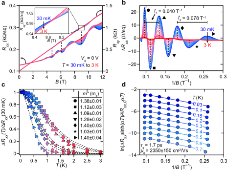
Figure 2a shows the temperature dependence of Rxx(B) and Rxy(B) for Vg = 0 V and Fig. 2b shows Rxx subtracted a background (SM Fig. S2), Rxx, as a function of 1/B for different temperatures. The amplitudes of the SdH oscillations clearly reduce upon heating and the carrier effective mass, m∗, is extracted by fitting the temperature dependent term in the Ando relation Ando et al. (1982): Rxx(T)/Rxx(T0) = Tsinh(T0)/T0sinh(T), where T0 = 30 mK, = 2/, = eB/m∗, and is the Boltzmann constant (Fig. 2c). The effective mass, m∗, is found to be between 1.03 and 1.40 m, similar to typical values reported for all-crystalline LAO/STO interfaces Caviglia et al. (2010a); Ben Shalom et al. (2010); Xie et al. (2014). Also apparent in Fig. 2b are two different 1/B frequencies, f1 = 0.040 T-1 and f2 = 0.078 T-1 differing by a factor of 2 consistent with a transition from an apparent spin degenerate to a fully spin resolved electronic system at B 6 T (SM Fig. S3). Note that this apparent spin degeneracy is different from that found in conventional semiconductors due to the much larger effective mass in oxides leading to a Landau level (LL) splitting, , comparable with the Zeeman splitting, ( is the g factor and the Bohr magneton). Using a g factor Laguta et al. (2002); Caviglia et al. (2010b) of 2, the Zeeman and LL splitting energies (for m∗ = 1.30 m) at B = 6 T become 0.70 and 0.54 meV, respectively. In this case, the intrinsic spin degeneracy should be lifted at all fields where SdH oscillations are observed. However, at low magnetic fields, an apparent spin degeneracy occurs when the spin-down part of LL n overlaps with the spin-up part of LL n + 1 (SM Fig. S3). Thus, the system becomes spin resolved only at fields above 6 T. For a spin resolved electronic system without valley degeneracy, this leads to a n = /(f1h) 5.91011 cm-2, which remarkably is 10 times lower than n similar to other STO-based interfaces Chen et al. (2013); Caviglia et al. (2010a); Ben Shalom et al. (2010); Xie et al. (2014); McCollam et al. (2014); Son et al. (2010). The quantum mobility, , is extracted in Fig. 2d by plotting the 1/B dependency of the absolute reduction of the oscillation amplitude using the Dingle formula Coleridge et al. (1989): ln[(Rxx(B)sinh(T))/(4Rxx(B=0T)T)], where = 2/, = eB/m∗, and Rxx(B=0T) = 128 /sq. These Dingle plots reveal a of 2350 cm2/V s (see Fig. 2d). This quantum mobility is approximately 1 order of magnitude higher than that for all-crystalline LAO/STO interfaces Caviglia et al. (2010a); Ben Shalom et al. (2010); Xie et al. (2014), and comparable to that in the spinel/perovskite -Al2O3/SrTiO3 interface Chen et al. (2013).
When tilting the magnetic field angle the oscillation amplitudes decrease rapidly with the SdH oscillations almost disappearing at angles above 40∘, consistent with the electronic system being strongly confined at the interface (SM Figs. S4 and S5).
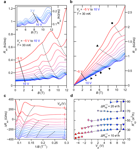
The Rxx(B) and Rxy(B) traces change significantly as Vg is varied from to 10 V (see Figs. 3a and 3b). Specifically, n changes from 3.01012 to 7.81012 cm-2 and from 5760 to 11,416 cm2/V s for Vg = V to 10 V (SM Figs. S6a and S6b). For the different Vg, Rxx shows clear oscillations with a 1/B periodicity (see Fig. 3c) and extracting the spin resolved SdH oscillation frequency for the different Vg results in n changing from 3.81011 cm-2 to 8.51011 cm-2 for Vg = to 10 V (SM Fig. S6c). Notably, n remains 10n in the full range of investigated Vg (SM Fig. S6d). Remarkably, the Hall resistance develops a steplike behavior with well-defined quantum Hall plateaus upon increasing Vg (see Fig. 3b). All Hall resistance plateaus, chosen to be at the minimum position of dRxy/dB, coincide with minima in Rxx and Fig. 3d shows the value of 1/Rxy at the plateaus in units of e2/h as a function of Vg. Strikingly, R does not appear to assume integer values of e2/h different from QHE in the conventional semiconductor quantum well comprising a single band where R = (SM, Sec. 1). Moreover, R for the same plateau varies as a function of Vg, contrary to the case in conventional semiconductors where it remains constant Klitzing et al. (1980). The plateaus, however, appear regularly spaced for all Vg with either 10 or 20 for B 6 T and B 6 T, respectively. Assuming a spin resolved or apparent spin degenerate situation where = 1 or 2, respectively, the inverse Hall resistance at plateaus is spaced by = N, where N = 10 and = 1.00.2. The overall linearity of the Hall resistance and the relative flatness of the Hall plateaus at high Vg and magnetic field suggest that the contribution from a low-mobility parallel conducting channel is negligible. And indeed, the scaling factor N 102 remains the same when considering the contribution from a low-mobility parallel conducting channel van der Burgt et al. (1995); Grayson and Fischer (2005) not in the SdH regime (SM, Figs. S7–S9). Xie et al. observed quantizationlike Hall resistance at the LAO/STO interface Xie et al. (2014) with a spacing that scaled with N 4. This was explained by a breaking of the fundamental band symmetry through magnetic breakdown orbits; however, this explanation cannot account for a scaling factor of N 102 observed here. A consistent description of the data, however, appears if we recognize that the modulation-doped oxide interface may consist of multiple parallel conducting channels that collectively give rise to a combined QHE Cao et al. (2012); Störmer et al. (1986). For instance, conduction through highly doped Bi2Se3 occurs through multiple quantum wells, and gives rise to quantized Hall resistance plateaus with R = N where = 1.00.2 and N is the number of quantum wells Cao et al. (2012). However, in that case the quantum wells are almost uncoupled with identical charge carrier densities and almost behave like a classic Kronig-Penney model. On the other hand, due to band bending in STO, the charge carrier density in our parallel electronic channels is expected to vary across the different channels Son et al. (2009); Khalsa and MacDonald (2012); Reich et al. (2015) and the R quantization is not expected to assume integer values of . This is a consequence of the measured filling factor, (B), being an average of the filling factors of each channel, (B), which take integer values at different B fields owing to their different carrier densities. Furthermore, the different (B) likewise explain why well-defined plateaus are only observed for certain carrier density combinations where (B) are near multiples of each other (SM, Sec. S1). However, the step size, , between plateaus is expected to take integer values of N (SM, Sec. S1) where N is the number of parallel conducting channels.
In order to quantitatively address whether such parallel electronic channels with varying charge carrier density can account for the observed Rxx oscillations and Rxy plateaus, the data are fitted (SM, Sec. S2 and Figs. S10 and S11) by summing contributions from N = 10 parallel conducting channels that are either apparent spin degenerate (for B6 T) or spin resolved (for B6 T). Here, the analytical expression for Rxx,i oscillations of each channel (i=1,2,3,…,10) with charge carrier density ni is given by Coleridge et al. (1989)
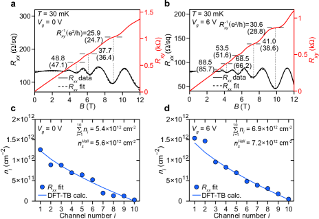
For Vg = 0 and 6 V (see Figs. 4a and 4b), there is an excellent agreement between the measured Rxx oscillations subtracted a magnetoresistance background and the calculated Rxx traces with fitted values of ni as illustrated in Figs. 4c and 4d. Furthermore, R calculated using the fitted charge carrier densities agrees well with the measured plateau values for both Vg = 0 and 6 V (Figs. 4a and 4b). Importantly, the obtained set of charge carrier densities consistently predicts not only the observed steps of 102 or 202 but also the unconventional R variation observed in Fig. 3d for the two Vg considered. Ultimately, we believe that this physical picture is representable for the entire gate-voltage range investigated, i.e., that the ten parallel conducting electronic channels are responsible for the observed Rxx oscillations and Rxy plateaus from Vg = to 10 V. In other words, the modulation-doped oxide interface consists of multiple parallel conducting two-dimensional channels with similar effective mass, Hall mobility, and quantum mobility, whereas the charge carrier density of different channels varies greatly. Upon application of an electric field all channels populate (deplete) concurrently with the same normalized gate dependence (). Moreover, the number of channels is expected to increase (decrease) when the electronic system is populated/depleted sufficiently beyond the investigated gate-voltage range of Vg = to 10 V and will be the subject of future studies. This physical picture is consistent with recent experiments on strongly carrier depleted LAO/STO Pallecchi et al. (2015).
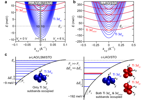
To further understand the nature of the parallel conducting channels, DFT-TB calculations are performed considering a wedge-shaped triangular quantum well (SM, Sec. S3). Figure 5a shows the obtained charge carrier dispersions for Vg = 0 and 6 V (left and right panels, respectively). These calculations support, for both Vg = 0 and 6 V, the existence of ten occupied Ti 3dxy sub-bands that have similar effective mass, Hall mobility, and quantum mobility, and calculated charge carrier densities that are consistent with the experimental data (see Figs. 4c and d). Therefore, our modulation-doped oxide interface, a single quantum well with multiple occupied Ti 3dxy sub-bands (see Fig. 5c), is quite different from what is found in the canonical LAO/STO interface, for n 1.71013 cm-2 where all t2g levels (both Ti 3dxy and 3dxz/yz sub-bands) are usually occupied in the quantum well (see Figs. 5b and 5c). This difference is caused by a much lower carrier density in a-LAO/LSM/STO compared to LAO/STO due to the LSM spacer layer in the former case acting as an electron acceptor Chen et al. (2015). With a reduced carrier density of 1012 cm-2 in a-LAO/LSM/STO, the slope of the confining potential is consequently much lower, resulting in a shallower well compared to other STO-based systems such as LAO/STO (see Fig. 5c). With the prevailing population of sub-bands, the Rashba spin-orbital interaction is expected to be much weaker in our modulation-doped interface compared to the LAO/STO interface with orbital-mixing character Fête et al. (2014). Importantly, the multiple parallel conducting two-dimensional sub-bands differentiate complex oxides, particularly our modulation-doped oxide interface, from conventional semiconductor 2-DEGs with the potential of exploring unusual and exotic physics based on STO.
In summary, we present the observation of quantized Hall resistance with integer step size in two-dimensional conducting complex oxide interfaces based on the patterned a-LAO/LSM/STO structure, revealing that the complex oxide interface consists of a single quantum well with multiple parallel Ti 3dxy sub-bands. Importantly, as the electrons are confined in STO, the multiple-subband physical picture is expected to be a common feature of all STO-based conducting systems. This insight paves the way for demonstrating new physics in devices based on complex oxide interfaces.
Acknowledgements.
The authors gratefully acknowledge the discussions with A. Smith, J. Levy, S. Ilani, J. Folk, S.L. Folk, G.B.S. Khalsa, and M. Schecter, and the technical assistance from J. Geyti, N. Payami, C.B. Sørensen, S. Upadhyay, C. Olsen, and A. Jellinggaard. Funding from the Danish Agency for Science, Technology and Innovation, and the Lundbeck Foundation are acknowledged. The Center for Quantum Devices is supported by the Danish National Research Foundation.References
- Klitzing et al. (1980) K. v. Klitzing, G. Dorda, and M. Pepper, Physical Review Letters 45, 494 (1980).
- Tsui et al. (1982) D. C. Tsui, H. L. Stormer, and A. C. Gossard, Physical Review Letters 48, 1559 (1982).
- Cao et al. (2012) H. Cao, J. Tian, I. Miotkowski, T. Shen, J. Hu, S. Qiao, and Y. P. Chen, Physical Review Letters 108, 216803 (2012).
- Zhang et al. (2005) Y. Zhang, Y.-W. Tan, H. L. Stormer, and P. Kim, Nature 438, 201 (2005).
- Tsukazaki et al. (2007) A. Tsukazaki, A. Ohtomo, T. Kita, Y. Ohno, H. Ohno, and M. Kawasaki, Science 315, 1388 (2007).
- Tsukazaki et al. (2010) A. Tsukazaki, S. Akasaka, K. Nakahara, Y. Ohno, H. Ohno, D. Maryenko, A. Ohtomo, and M. Kawasaki, Nature Materials 9, 889 (2010).
- Ohtomo and Hwang (2004) A. Ohtomo and H. Y. Hwang, Nature 427, 423 (2004).
- Chen et al. (2013) Y. Z. Chen, N. Bovet, F. Trier, D. V. Christensen, F. M. Qu, N. H. Andersen, T. Kasama, W. Zhang, R. Giraud, J. Dufouleur, T. S. Jespersen, J. R. Sun, A. Smith, J. Nygård, L. Lu, B. Büchner, B. G. Shen, S. Linderoth, and N. Pryds, Nature Communications 4, 1371 (2013).
- Falson et al. (2015) J. Falson, D. Maryenko, B. Friess, D. Zhang, Y. Kozuka, A. Tsukazaki, J. H. Smet, and M. Kawasaki, Nature Physics 11, 347 (2015).
- Thiel et al. (2006) S. Thiel, G. Hammerl, A. Schmehl, C. W. Schneider, and J. Mannhart, Science 313, 1942 (2006).
- Christensen et al. (2013) D. V. Christensen, F. Trier, Y. Z. Chen, A. Smith, J. Nygård, and N. Pryds, Applied Physics Letters 102, 021602 (2013).
- Reyren et al. (2007) N. Reyren, S. Thiel, A. D. Caviglia, L. F. Kourkoutis, G. Hammerl, C. Richter, C. W. Schneider, T. Kopp, A.-S. Ruetschi, D. Jaccard, M. Gabay, D. A. Muller, J.-M. Triscone, and J. Mannhart, Science 317, 1196 (2007).
- Caviglia et al. (2008) A. D. Caviglia, S. Gariglio, N. Reyren, D. Jaccard, T. Schneider, M. Gabay, S. Thiel, G. Hammerl, J. Mannhart, and J.-M. Triscone, Nature 456, 624 (2008).
- Brinkman et al. (2007) A. Brinkman, M. Huijben, M. van Zalk, J. Huijben, U. Zeitler, J. C. Maan, W. G. van der Wiel, G. Rijnders, D. H. A. Blank, and H. Hilgenkamp, Nature Materials 6, 493 (2007).
- Sulpizio et al. (2014) J. A. Sulpizio, S. Ilani, P. Irvin, and J. Levy, Annual Review of Materials Research 44, 117 (2014).
- Delugas et al. (2011) P. Delugas, A. Filippetti, V. Fiorentini, D. I. Bilc, D. Fontaine, and P. Ghosez, Physical Review Letters 106, 166807 (2011).
- Son et al. (2009) W.-J. Son, E. Cho, B. Lee, J. Lee, and S. Han, Physical Review B 79, 245411 (2009).
- Khalsa and MacDonald (2012) G. Khalsa and A. H. MacDonald, Physical Review B 86, 125121 (2012).
- Breitschaft et al. (2010) M. Breitschaft, V. Tinkl, N. Pavlenko, S. Paetel, C. Richter, J. R. Kirtley, Y. C. Liao, G. Hammerl, V. Eyert, T. Kopp, and J. Mannhart, Physical Review B 81, 153414 (2010).
- Joshua et al. (2012) A. Joshua, S. Pecker, J. Ruhman, E. Altman, and S. Ilani, Nature Communications 3, 1129 (2012).
- Gabay and Triscone (2013) M. Gabay and J.-M. Triscone, Nature Physics 9, 610 (2013).
- Caviglia et al. (2010a) A. D. Caviglia, S. Gariglio, C. Cancellieri, B. Sacépé, A. Fête, N. Reyren, M. Gabay, A. F. Morpurgo, and J.-M. Triscone, Physical Review Letters 105, 236802 (2010a).
- Ben Shalom et al. (2010) M. Ben Shalom, A. Ron, A. Palevski, and Y. Dagan, Physical Review Letters 105, 206401 (2010).
- Xie et al. (2014) Y. Xie, C. Bell, M. Kim, H. Inoue, Y. Hikita, and H. Y. Hwang, Solid State Communications 197, 25 (2014).
- McCollam et al. (2014) A. McCollam, S. Wenderich, M. K. Kruize, V. K. Guduru, H. J. A. Molegraaf, M. Huijben, G. Koster, D. H. A. Blank, G. Rijnders, A. Brinkman, H. Hilgenkamp, U. Zeitler, and J. C. Maan, APL Materials 2, 022102 (2014).
- Son et al. (2010) J. Son, P. Moetakef, B. Jalan, O. Bierwagen, N. J. Wright, R. Engel-Herbert, and S. Stemmer, Nature Materials 9, 482 (2010).
- Chen et al. (2015) Y. Z. Chen, F. Trier, T. Wijnands, R. J. Green, N. Gauquelin, R. Egoavil, D. V. Christensen, G. Koster, M. Huijben, N. Bovet, S. Macke, F. He, R. Sutarto, N. H. Andersen, J. A. Sulpizio, M. Honig, G. E. D. K. Prawiroatmodjo, T. S. Jespersen, S. Linderoth, S. Ilani, J. Verbeeck, G. Van Tendeloo, G. Rijnders, G. A. Sawatzky, and N. Pryds, Nature Materials 14, 801 (2015).
- Trier et al. (2015) F. Trier, G. E. D. K. Prawiroatmodjo, M. von Soosten, D. V. Christensen, T. S. Jespersen, Y. Z. Chen, and N. Pryds, Applied Physics Letters 107, 191604 (2015).
- Schneider et al. (2006) C. W. Schneider, S. Thiel, G. Hammerl, C. Richter, and J. Mannhart, Applied Physics Letters 89, 122101 (2006).
- Coleridge et al. (1989) P. T. Coleridge, R. Stoner, and R. Fletcher, Physical Review B 39, 1120 (1989).
- Zhong et al. (2013) Z. Zhong, Q. Zhang, and K. Held, Physical Review B 88, 125401 (2013).
- Stornaiuolo et al. (2012) D. Stornaiuolo, S. Gariglio, N. J. G. Couto, A. Fête, A. D. Caviglia, G. Seyfarth, D. Jaccard, A. F. Morpurgo, and J.-M. Triscone, Applied Physics Letters 101, 222601 (2012).
- Ando et al. (1982) T. Ando, A. B. Fowler, and F. Stern, Rev. Mod. Phys. 54, 437 (1982).
- Laguta et al. (2002) V. V. Laguta, M. D. Glinchuk, R. O. Kuzian, S. N. Nokhrin, I. P. Bykov, J. Rosa, L. Jastrabik, and M. G. Karkut, Journal of Physics: Condensed Matter 14, 13813 (2002).
- Caviglia et al. (2010b) A. D. Caviglia, M. Gabay, S. Gariglio, N. Reyren, C. Cancellieri, and J.-M. Triscone, Physical Review Letters 104, 126803 (2010b).
- van der Burgt et al. (1995) M. van der Burgt, V. C. Karavolas, F. M. Peeters, J. Singleton, R. J. Nicholas, F. Herlach, J. J. Harris, M. Van Hove, and G. Borghs, Physical Review B 52, 12218 (1995).
- Grayson and Fischer (2005) M. Grayson and F. Fischer, Journal of Applied Physics 98, 013709 (2005).
- Störmer et al. (1986) H. L. Störmer, J. P. Eisenstein, A. C. Gossard, W. Wiegmann, and K. Baldwin, Phys. Rev. Lett. 56, 85 (1986).
- Reich et al. (2015) K. V. Reich, M. Schecter, and B. I. Shklovskii, Physical Review B 91, 115303 (2015).
- Pallecchi et al. (2015) I. Pallecchi, F. Telesio, D. Li, A. Fête, S. Gariglio, J.-M. Triscone, A. Filippetti, P. Delugas, V. Fiorentini, and D. Marré, Nature Communications 6, 6678 (2015).
- Fête et al. (2014) A. Fête, S. Gariglio, C. Berthod, D. Li, D. Stornaiuolo, M. Gabay, and J.-M. Triscone, New Journal of Physics 16, 112002 (2014).