Atom-atom interactions around the band edge of a photonic crystal waveguide
Abstract
Tailoring the interactions between quantum emitters and single photons constitutes one of the cornerstones of quantum optics. Coupling a quantum emitter to the band edge of a photonic crystal waveguide (PCW) provides a unique platform for tuning these interactions. In particular, the crossover from propagating fields outside the bandgap to localized fields within the bandgap should be accompanied by a transition from largely dissipative atom-atom interactions to a regime where dispersive atom-atom interactions are dominant. Here, we experimentally observe this transition for the first time by shifting the band edge frequency of the PCW relative to the line of atomic cesium for atoms trapped along the PCW. Our results are the initial demonstration of this new paradigm for coherent atom-atom interactions with low dissipation into the guided mode.
pacs:
42.50.Ct, 42.50.Nn, 37.10.Gh, 42.70.QsRecent years have witnessed a spark of interest in combining atoms and other quantum emitters with photonic nanostructures LMS15 . Many efforts have focused on enhancing emission into preferred electromagnetic modes relative to vacuum emission, thereby establishing efficient quantum matter-light interfaces and enabling diverse protocols in quantum information processing K08 . Photonic structures developed for this purpose include high-quality cavities VY03 ; YSH04 ; ADW06 ; HBW07 ; TTL13 , dielectric fibers BHB09 ; BHK04 ; LVB09 ; VRS10 ; GCA12 ; polzik , metallic waveguides CSD07 ; AMY07 ; HKS11 , and superconducting circuits WSB04 ; VFL13 ; DS13 . Photonic crystal waveguides (PCWs) are of particular interest since the periodicity of the dielectric structure drastically modifies the field propagation, yielding a set of Bloch bands for the guided modes JMW95 . For example, recent experiments have demonstrated superradiant atomic emission due to a reduction in group velocity for an atomic frequency near a band edge of a PCW GHH15 .
A quite different paradigm for atom-light interactions in photonic crystals was proposed in Refs. Y1987 ; J1987 ; JW1990 ; K1990 , but has yet to be experimentally explored. In particular, when an atomic transition frequency is situated within a bandgap of a PCW, an atom can no longer emit propagating waves into guided modes (GMs) of the structure. However, an evanescent wave surrounding the atoms can still form, resulting in the formation of atom-photon bound states shi ; calajo . This phenomenon has attracted new interest recently as a means to realize dispersive interactions between atoms without dissipative decay into GMs. The spatial range of atom-atom interactions is tunable for D and D PCWs and set by the size of the photonic component of the bound state DHH15 ; GHC15 . Many-body physics with large spin exchange energies and low dissipation can thereby be realized, in a generalization of cavity QED arrays HBP06 ; GTC06 . Fueled by such perspectives, there have been recent experimental observations with atoms GHH15 ; GHY14 ; YHM14 and quantum dots LSJ08 ; YTB15 interacting through the GMs of photonic crystal waveguides, albeit in frequency regions outside the bandgap, where GMs are propagating fields.
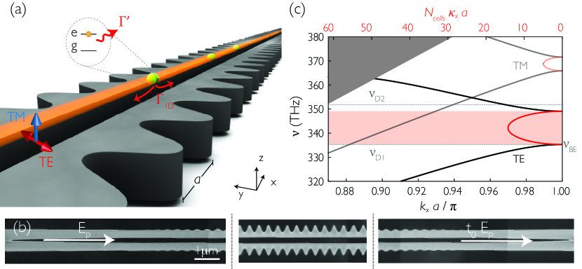
In this manuscript, we report the first observation of collective dispersive shifts of the atomic resonance around the band edge of a photonic crystal. Thermal tuning allows us to control the offset of the band edge frequency () of the PCW relative to frequency of the line of cesium. In both the dispersive domain (i.e., outside the bandgap with electric field ) and reactive regime (i.e., inside the bandgap with ), we record transmission spectra for atoms trapped along the PCW, as illustrated in Fig. 1(a).
To connect the features of the measured transmission spectra to underlying atom-atom radiative interactions, we have developed a formalism based on the electromagnetic Green’s function. The model allows us to infer the peak single-atom frequency shift of the atomic resonance and guided mode decay rate as functions of detuning between the atomic and band edge frequencies. From the observation of superradiant emission outside the bandgap, we infer the average number of trapped atoms to be , as described in Ref. GHH15 and the supporting material SM . For frequencies inside the bandgap ( GHz) the ratio of dissipative to coherent rates is , due to the exponential localization of the atomic radiation in the bandgap. For comparison, the prediction for our system from cavity quantum electrodynamics (CQED) models alone is . Besides yielding a more favorable ratio between coherent and dissipative guided mode rates, PCWs offer significant advantages when compared to conventional cavities as platforms for atom-light interfaces. First, the range of interaction in a PCW is tunable, ranging from effectively infinite to nearest neighbor, in contrast to the fixed infinite range of a cavity. Second, due to the multimode nature of PCWs, one can employ different guided modes as different interaction channels to which the atoms simultaneously couple.
Alligator Photonic Crystal Waveguide - Figure 1(a) provides an overview of our experiment with atoms trapped near and strongly interacting with the TE-like mode of an alligator PCW. The suspended silicon nitride structure consists of nominally identical unit cells of lattice constant nm, and is terminated by tapering cells on each side, as shown in the SEM images in Fig. 1(b). The tapers mode-match the fields of the PCW to the fields of uncorrugated nanobeams for efficient input and output coupling. Design, fabrication, and characterization details are described in Refs. YHM14 ; GHY14 ; GHH15 . Figure 1(c) shows the nominal cell dispersion relations for the TE (polarized mainly along ) and TM-like modes (polarized mainly along ). After release of the SiN structure from the Si substrate, a low power CF4 etch is used to align the lower/‘dielectric’ TE band edge () to the Cs transition (). The TM mode has band edges far detuned from the both the Cs and lines. In our experiment, the TE mode is used to probe the atoms, while the TM mode with approximately linear dispersion serves to calibrate the density and trap properties.
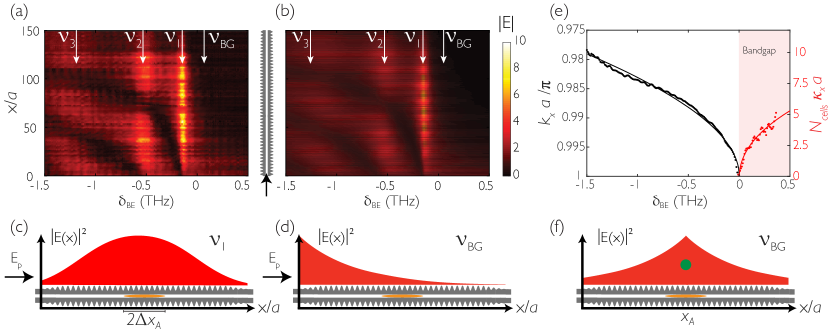
In order to better understand atomic interactions with the PCW, it is helpful to visualize the spatial profile of the fields generated absent atoms, when light is input from one end. Figure 2(a) shows the measured intensity along the length of the PCW as a function of probe detuning around the band edge, where is the probe frequency. The intensity was measured by imaging weak scatterers along the length of the alligator PCW that, after calibration, serve as local probes of the intensity SM . Figure 2(b) shows the corresponding finite-difference time-domain (FDTD) simulated intensity Lumerical . In both images, resonances appear at due to the weak cavity formed by the reflections of the tapers. The spatial modulation of the intensity at the resonances due to the cavity effect is approximated by , where is the effective wave-vector near the band edge. The ’th resonance at frequency is such that , where is the effective length of the PCW (including field penetration into the tapers). Fig. 2(c) shows a plot of for a probe input at frequency at the first resonance. Inside the bandgap () the field is evanescent, and . Fig. 2(d) plots for probe frequency inside the bandgap, and shows the exponential decay of the intensity. Using a model for the field in a finite photonic crystal SM , we fit the measured intensity for each frequency in Fig. 2(a) and Fig. 2(b) and extract and , thereby obtaining the dispersion relations shown in Fig. 2(e). Importantly, we determine the band edge frequency for the actual device to be GHz relative to the readily measured first resonance at , which is in good agreement with the FDTD simulated result of GHz.
Both are relevant to our measurements of transmission spectra with trapped atoms. The presence of a ‘cavity’ mode at implies that the emission of an atom with transition frequency will generate a field inside the PCW with a similar spatial profile to that of the cavity mode, as shown in Fig. 2(c). By contrast, atomic emission in the regime with within the bandgap will excite an exponentially localized mode centered around , as illustrated in Fig. 2(f).
Experiment.– Cs atoms are trapped above the surface of the alligator PCW, as shown in Fig. 1(a), using a similar experimental setup to that reported in Ref. GHH15 . As described in more detail in the previous reference, the decay rate into the guided mode is exponentially sensitive to the trap position above the surface of the alligator PCW. Our calculations and measurements of agree with COMSOL simulations COMSOL of the trap position, and thus we are able to determine that the Cs atoms are trapped nm above the surface of the alligator PCW. Atoms are cooled and trapped in a MOT around the PCW, and then loaded into a dipole trap formed by the reflection from the device of a frequency red-detuned side illumination (SI) beam. The SI beam has a waist of m, and the polarization is aligned along the axis for maximum reflection from the PCW. We measure a trap life time of ms, and we estimate an atom temperature of K from time-of-flight measurements. From the trap simulations (for details see supporting materials SM ), we infer that the atoms are confined to a region nm above the surface with dimensions m, nm. The simulations predict that more energetic atoms escape the trap and collide into the structure, since the weakest direction of the trap is along the diagonals of the - plane due to Casimir-Polder forces.
In order to estimate the average number of trapped atoms, we measure the superradiant atomic decay rate when the atom frequency is tuned to the first resonance of the PCW (Fig. 2(c)) GHH15 . Due to the strong dissipative interactions between the atoms and with , the collective decay rate is enhanced as compared to the single atom decay rate, and we infer an average atom number of SM . In the low density limit , the measured decay rate corresponds to that of a single atom. We then measure a guided mode decay rate , which is in good agreement with the FDTD simulations at the calculated trap location SM .
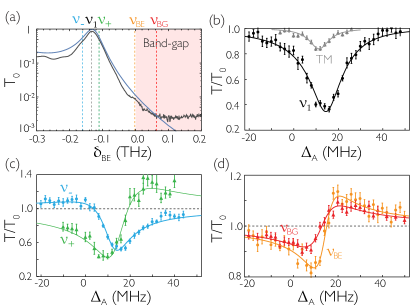
After the atoms are loaded into the trap, we send a weak 5 ms probe beam with frequency in either the TE or TM guided mode through the PCW and record the transmitted intensity . The probe beam scans near the Cs transition. Each experimental cycle runs at a fixed detuning relative to the free-space atomic transition frequency . We observe little change of signal during the ms probing time, suggesting that the atom number is approximately constant over this interval. The band edge of the PCW is tuned thermally by shining an external laser onto a corner of the chip, where its light is absorbed by the silicon substrate. Hence, the Cs line can be aligned to be either outside or inside the bandgap with an uncertainty GHz. The transmission for each data point is normalized by the transmission with no atoms (), resulting in a measurement of . The logarithm of the measured and simulated transmission spectrum with no atoms is shown in Fig. 3(a).
Examples of transmission spectra with atoms are shown in Figs. 3(b-d). Note that the spectra are shifted 12.5 MHz due to both the AC Stark shift of the dipole trap and the modified Lamb shift induced by the non-guided modes of the PCW. Notably, the transmission spectra at the first ‘cavity’ resonance exhibit a characteristic Lorentzian ‘dip’, and they become more and more asymmetric as the frequency moves into the bandgap.
Transmission model.– We have developed a model to extract quantitative values for collective decay rates and frequency shifts from these atomic transmission spectra AHC16 . While the formalism of waveguide SF05 and cavity QED GC85 is well suited for describing atoms coupled to uniform waveguides and cavities, it is not general enough to capture the rich physics of atomic interactions in the vicinity of a PCW. Instead, we describe our system by employing a spin model in terms of the classical electromagnetic Green’s function, in which the atoms (or ‘pseudo-spins’ for ground and excited state) interact via the emission and re-absorption of guided photons DKW02 ; BW07 ; DSF10 .
The electromagnetic Green’s function is related to the electric field emitted by a dipole oscillating at frequency at position by NH06 ; BW07 . The dipole moment operator for atom is decomposed into , where is the dipole matrix element, and where is the atomic coherence operator between the ground and excited states. The spin model describes a system of atoms coupled to and driven by a guided mode of the PCW. In the low saturation and steady-state regime, expectation values for the atomic coherences () are described by a linear system of equations AHC16 ; SM
| (1) |
where is the detuning between the probe and the atomic angular frequencies, is the classical drive (Rabi frequency) for the ’th atom due to the guided mode input field, and where , and . Each atom can also decay into non-guided modes, including free-space, with a decay rate . The appearance of the real and imaginary parts of the Green’s function in the coherent and dissipative terms has the classical analogue that the in-phase and out-of-phase components of a field with respect to an oscillating dipole store time-averaged energy and perform time-averaged work, respectively. Since the first term in (S7) is diagonal, the atomic coherences can be understood in terms of the eigenvalues for and eigenfunctions of the matrix , whose elements are . The real and imaginary parts of correspond to frequency shifts and guided mode decay rates, respectively, of the collective atomic mode .
The transmission spectrum can be expressed in terms of the eigenvalues of as SM ; AHC16 ,
| (2) |
where is the transmission without atoms. In the case of a single atom, the only eigenvalue is proportional to the self-Green’s function, , which implies that the transmission spectrum is a direct measurement of the self-Green’s function at the atom’s position. For non-interacting atoms, the off-diagonal elements of are zero, and thus the eigenvalues are single-atom quantities, as there is no cooperative response.
In contrast, for interacting atoms, the off-diagonal elements are non-negligible, and there is a cooperative response. In particular, for the atomic frequency inside the bandgap of a photonic crystal, the elements are well approximated by DHH15
| (3) |
where the cosine factors arise from the Bloch mode and the decay length is due to the exponential decay of the field and results in a finite range of interaction. For an infinite photonic crystal, , since the light is localized and there is no dissipation through the guided mode. But for a finite PCW of length , the guided mode dissipation is finite due to leakage of the mode out of the edges of the structure.
In the limit where the interaction range is much larger than the separation of the atoms, , the guided mode input field couples predominantly to a single collective “bright” mode of the system with eigenvalue . Formally, when , the matrix is separable [ with ] and therefore only has one non-zero eigenvalue. In this single bright mode approximation, the transmission spectrum is given by
| (4) |
We have confirmed numerically that this single ‘bright mode’ picture is valid within the limits of our uncertainties for the range of frequencies of the measured spectra in Fig. 3 In particular, at the largest detuning into the bandgap GHz, we have . However, for atomic frequencies further away from the band edge, this approximation eventually breaks down (e.g., at the bandgap center, ).
The single bright mode approximation is also valid in conventional cavity QED. The Green’s function matrix is then given by , where is the wave-vector of the standing-wave cavity. In this case, and , where is the detuning from the cavity resonance and is the cavity linewidth. Importantly, the ratio between the imaginary dissipative coupling rate to the real coherent coupling rate falls off with inverse detuning, for large , whereas in a PCW bandgap, the fall off is exponential with detuning from the band edge.
Analysis of measured spectra– Equation (4) provides a direct mapping between the observed transmission spectra of Figs. 3(b-d) and the electromagnetic Green’s function of the PCW. In particular, the line shape is Lorentzian for purely dissipative dynamics (). This is precisely what occurs at the frequency of the first cavity mode , as shown by Fig. 3(b). When the GM band edge frequency is moved towards the atomic resonance , the dispersive interactions are switched on, and the transmission line shape becomes asymmetric, displaying a Fano-like resonance F1961 , as can be observed in Figs. 3(c,d). The appearance of an asymmetry in the atomic spectra directly reveals a significant coherent coupling rate , which is evident for frequencies that lie in the bandgap region.
For all relevant frequencies, the spectra for the TM guided mode are approximately symmetric, as for this GM polarization. An example of a TM spectrum is shown in the gray curve of Fig. 3(b). Since the TM bandgap is so far detuned, the TM spectra are insensitive to and serve as a calibration signal. Using a waveguide transmission model, we fit the TM transmission spectra and extract a TM guided mode decay rate of . This rate is times smaller than the TE guided mode decay rate at the first resonance . The ratio is explained well by the expected slow-light and cavity enhancement of the PCW described in Ref. GHH15 and supporting material SM . From the TM fits, we also measure MHz, which, due to inhomogeneous broadening, is larger than value MHz from FDTD numerical calculations SM . While tuning the band edge to move the atomic frequency into in the bandgap, TM spectra are measured in order to confirm in situ that the average atom number is approximately constant over the course of the measurements of TE spectra.
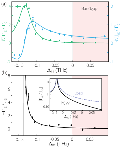
To obtain quantitative values for the collective frequency shifts and decay rates by fitting the TE atomic spectra to the spin model, we must account for the fluctuations in atom number and position along the -axis. As depicted in Fig. 1(a) and Fig. 2(c), trapped atoms are aproximately free to move along the axis of the device SM . Their coupling rates are thus modulated by the fast oscillation of the Bloch function, which near the band edge is approximately given by (S11), and . Here and are the peak values. Further, although we know the average atom number atoms from independent decay-rate measurements SM , the atom number for each experiment follows an unknown distribution. To model the experimental transmission spectra such as in Fig. 3, we average the expression in (4) over the atom positions along the Bloch function and assume a Poisson distribution for the atom number . We extract peak values and , and plot the resulting cooperative rates and in Fig. 4(a). In particular, at the first resonance , the fitted single atom guided-mode decay rate is , which is in good agreement with the decay time measurements, SM . More generally, we find good agreement between our measurements and our model for the transmission, as shown in Fig. 3.
The ratio is shown in Fig. 4(b). Because of the evanescent nature of the field in the bandgap, decays exponentially with increasing detuning into the bandgap, , where DHH15 . As displayed in the inset, the ratio between the frequency shift and the GM decay rate diminishes much faster than would be the case in traditional settings such as CQED, for which , where is the cavity linewidth and is the detuning from the cavity resonance. Indeed, by performing an average of the last two measured frequencies in the bandgap, we obtain , whereas , where we have taken the cavity linewidth to be a value consistent with the linewidth of the first cavity mode of the PCW ( GHz). We can then infer that the ratio of dispersive to dissipative rates for guided mode atom-atom interactions (i.e., ) is significantly larger than is the case in conventional optical physics (e.g., CQED).
Beyond the detailed modeling involving (4) averaged over fluctuations in atom number and position, we also fit the spectra with a generic transmission model with no averaging, as shown in the supporting material SM . We find that the effective values for the guided mode decay rate and frequency shift are related to and in Fig. 4(a) by a simple scale factor related to the averaging of the Bloch function .
Despite favorable scaling between the collective frequency shifts and the guided mode decay rates, there is still one obstacle to overcome towards purely dispersive atomic interactions, namely atomic emission into non-guided modes (characterized by ). For the current PCW structure, the FDTD simulated value of this decay rate is GHH15 for the relevant frequencies of our experiment. Fortunately, it has been shown that suitable engineering of a wide variety of nanophotonic structures can lead to significant reductions in Hung13 . For example, Ref. LMS15 reviews possibilities to achieve .
Concluding remarks and outlook– In conclusion, we report the first observation of cooperative atom interactions in the bandgap of a photonic crystal waveguide. By tuning the band edge frequency of the photonic crystal waveguide, we are able to modify the interactions between the atoms that are trapped close to the device, reducing the dissipative relative to coherent coupling for frequencies inside the bandgap of the PCW. Equipped with a theoretical model based on the electromagnetic Green’s function of the alligator photonic crystal waveguide, we infer quantitative values for the collective frequency shifts and decay rates experienced by the atoms. Moreover, we infer a suppression of the dissipative interactions with respect to the coherent ones several times larger than is customarily obtained in AMO physics. This measurement provides the first stepping stone towards the realization of quantum many body physics in bandgap systems.
Moreover, near-term extensions of our experiment open the door to exploring new physical scenarios by employing atoms coupled to PCWs. By trapping the atoms at the center of the device with guided modes Hung13 , we expect a 6-fold increase to both coupling strengths and relative to . Moreover, by probing the atoms with the Cs line tuned to the upper band edge, where the intensity at the position of the atoms is larger, we expect a further improvement by a factor of two. Combining these two effects, we expect a significant enhancement of interactions via guided modes as compared to conventional free space interactions, namely . This could enable investigations of new paradigms for atom-photon interactions, such as the recently proposed multi-photon dressed states calajo ; shi .
Note added– After the submission of this manuscript, Ref. LH16 reported measurements of transmission spectra for a superconducting qubit placed within the bandgap of a microwave photonic crystal.
Acknowledgments–We gratefully acknowledge the contributions of O. J. Painter and his group, including for fabrication and clean-room facilities. We further acknowledge A. Burgers, C.-L. Hung, J. Laurat, M. J. Martin, A. C. McClung, J. A. Muniz, and L. Peng. Funding is provided by the DOD NSSEFF program, the AFOSR QuMPASS MURI, NSF Grant PHY-1205729 the ONR QOMAND MURI, and the IQIM, an NSF Physics Frontiers Center with support of the Moore Foundation. A. G. was supported by the Nakajima Foundation. A. A.-G. and M. L. were supported by the IQIM Postdoctoral Fellowship. A. A.-G. also acknowledges support from the Global Marie Curie Fellowship LANTERN (655701). S.-P. Y. acknowledges support from the International Fulbright Science and Technology Award. DEC acknowledges support from Fundacio Privada Cellex Barcelona, Marie Curie CIG ATOMNANO, MINECO Severo Ochoa Grant SEV-2015-0522, and ERC Starting Grant FoQAL.
References
- (1) Lodahl P, Mahmoodian S, Stobbe S (2015) Interfacing single photons and single quantum dots with photonic nanostructures. Rev. Mod. Phys. 87:347.
- (2) Kimble HJ (2008) The quantum internet. Nature 453:1023–1030.
- (3) Vuckovic J, Yamamoto Y (2003) Photonic crystal microcavities for cavity quantum electrodynamics with a single quantum dot. App. Phys. Lett. 82:2374–2376.
- (4) Yoshie T et al. (2004) Vacuum rabi splitting with a single quantum dot in a photonic crystal nanocavity. Nature 432:200–203.
- (5) Aoki T et al. (2006) Observation of strong coupling between one atom and a monolithic microresonator. Nature 443:671.
- (6) Hennessy K et al. (2007) Quantum nature of a strongly coupled single quantum dot-cavity system. Nature 445:896–899.
- (7) Thompson JD et al. (2013) Coupling a single trapped atom to a nanoscale optical cavity. Science 6137:1202–1205.
- (8) Bajcsy M et al. (2009) Efficient all-optical switching using slow light within a hollow fiber. Phys. Rev. Lett. 102:203902.
- (9) Balykin VI, Hakuta K, Kien FL, Liang JQ, Morinaga M (2004) Atom trapping and guiding with a subwavelength-diameter optical fiber. Phys. Rev. A 70:011401.
- (10) Londero P, Venkataraman V, Bhagwat AR, Slepkov AD, Gaeta AL (2009) Ultralow-power four-wave mixing with rb in a hollow-core photonic band-gap fiber. Phys. Rev. Lett. 103:043602.
- (11) Vetsch E et al. (2010) Optical interface created by laser-cooled atoms trapped in the evanescent field surrounding an optical nanofiber. Phys. Rev. Lett. 104:203603.
- (12) Goban A et al. (2012) Demonstration of a state-insensitive, compensated nanofiber trap. Phys. Rev. Lett. 109:033603.
- (13) Sørensen HL et al. (2016) arXiv:1601.04869.
- (14) Chang DE, Sørensen AS, Demler EA, Lukin MD (2007) A single-photon transistor using nanoscale surface plasmons. Nat. Phys. 3:807–812.
- (15) Akimov AV et al. (2007) Generation of single optical plasmons in metallic nanowires coupled to quantum dots. Nature 450:402–406.
- (16) Huck A, Kumar S, Shakoor A, Andersen UL (2011) Controlled coupling of a single nitrogen-vacancy center to a silver nanowire. Phys. Rev. Lett. 106:096801.
- (17) Wallraff A et al. (2004) Strong coupling of a single photon to a superconducting qubit using circuit quantum electrodynamics. Nature 431:162–167.
- (18) Van Loo AF et al. (2013) Photon-mediated interactions between distant artificial atoms. Science 342:1494–1496.
- (19) Devoret MH, Shoelkopf RJ (2013) Superconducting circuits for quantum information: an outlook. Science 339:1169–1174.
- (20) Joannopoulos JD, Meade RD, Winn JN (1995) Photonic Crystals: Molding the Flow of Light. (Princeton University Press, Singapore).
- (21) Goban A et al. (2015) Superradiance for atoms trapped along a photonic crystal waveguide. Phys. Rev. Lett. 115:063601.
- (22) Yablonovitch E (1987) Inhibited spontaneous emission in solid-state physics and electronics. Phys. Rev. Lett. 58:2059.
- (23) John S (1987) Strong localization of photons in certain disordered dielectric superlattices. Phys. Rev. Lett. 58:2486.
- (24) John S, Wang J (1990) Quantum electrodynamics near a photonic band gap: photon bound states and dressed atoms. Phys. Rev. Lett. 64:2418.
- (25) Kurizki G (1990) Two-atom resonant radiative coupling in photonic band structures. Phys. Rev. A 42:2915.
- (26) Shi T, Wu YH, González-Tudela A, Cirac JI (2015), arXiv:1512.072338.
- (27) Calajó G, Ciccarello F, Chang DE, Rabl P (2015), arXiv:1512.04946.
- (28) Douglas JS et al. (2015) Quantum many-body models with cold atoms coupled to photonic crystals. Nat. Photon. 9:326–331.
- (29) González-Tudela A, Hung CL, Chang DE, Cirac JI, Kimble HJ (2015) Subwavelength vacuum lattices and atom-atom interactions in two-dimensional photonic crystals. Nat. Photon. 9:320–325.
- (30) Hartmann MJ, Brandao FGSL, Plenio MB (2006) Strongly interacting polaritons in coupled arrays of cavities. Nat. Phys. 2:849–855.
- (31) Greentree AD, Tahan C, Cole JH, Hollenberg LCL (2006) Quantum phase transitions of light. Nat. Comm. 2:856–861.
- (32) Goban A et al. (2014) Atom-light interactions in photonic crystals. Nat. Comm. 5:3808.
- (33) Yu SP et al. (2014) Nanowire photonic crystal waveguides for single-atom trapping and strong light-matter interactions. App. Phys. Lett. 104:111103.
- (34) Lund-Hansen T et al. (2008) Experimental realization of highly efficient broadband coupling of single quantum dots to a photonics crystal waveguide. Phys. Rev. Lett. 101:113903.
- (35) Young AB et al. (2015) Polarization engineering in photonic crystal waveguides for spin-photon entanglers. Phys. Rev. Lett. 115:153901.
- (36) See accompanying Supplemental Material for a thorough description of the design and characterization of the photonic crystal waveguide; of how to obtain the attenuation coefficient and the band edge position of the PCW; of how to generate the atomic spectra fits; and of the measurements of atomic decay.
- (37) COMSOL, http://www.comsol.com.
- (38) Asenjo-Garcia A, Hood JD, Chang DE, Kimble HJ (2016) Atom-light interactions in quasi-1D dielectrics: a Green’s function perspective. http://arxiv.org/abs/1606.04977.
- (39) Lumerical Solutions, Inc., http://www.lumerical.com/tcad-products/fdtd/.
- (40) Sheng JT, Fan S (2005) Coherent photon transport from spontaneous emission in one-dimensional waveguides. Opt. Lett. 30:2001.
- (41) Dung HT, Knöll L, Welsch DG (2002) Resonant dipole-dipole interaction in the presence of dispersing and absorbing surroundings. Phys. Rev. A 66:063810.
- (42) Buhmann SY, Welsch DG (2007) Dispersion forces in macroscopic quantum electrodynamics. Prog. Quantum Electron. 31:51.
- (43) Dzsotjan D, Sørensen AS, Fleischhauer M (2010) Quantum emitters coupled to surface plasmons of a nanowire: A Green’s function approach. Phys. Rev. B 82:075427.
- (44) Gardiner CW, Collet MJ (1985) Input and output in damped quantum systems: Quantum stochastic differential equations and the master equation. Phys. Rev. A 31:3761.
- (45) Novotny L, Hecht B (2006) Principles of Nano-Optics. (Cambridge University Press, New York).
- (46) Fano U (1961) Effects of configuration interaction on intensities and phase shifts. Phys. Rev. 124:1866–1878.
- (47) Hung C.-L., Meenehan SM, Chang DE, Painter O, Kimble HJ, (2013). Trapped atoms in one-dimensional photonic crystals. New J. Phys. 15: 083026.
- (48) Liu Y and Houck AA (2016) Quantum electrodynamics near a photonic band-gap, arXiv:1603.02998.
Supplemental Information: Atom-atom interactions around the band edge of a photonic crystal waveguide
I Introduction
In our results of the main text, we measure collective frequency shifts and decay rates for atoms trapped near a photonic crystal waveguide (PCW). In our previous work in Ref. GHH15 , we trapped multiple atoms in an optical dipole-force trap above the PCW. We operated with the atomic frequency outside the bandgap in a regime with large decay rate and small coherent coupling rate . By varying the density and observing the superradiant decay of the atoms , we inferred the single-atom guided-mode decay rate and the average number of atoms . Importantly, this measured single-atom decay rate agreed well with the finite-difference time-domain (FDTD) simulations at the calculated trap location. This good agreement is in part due to the nanometer-scale accuracy in which the alligator PCWs are fabricated, which is required for both the band-edge alignment and the device quality.
In our current manuscript, the band-edge of the PCW is tuned around the resonance frequency of the atoms, and we observe the dominance of the guided-mode coherent coupling rates over the dissipative coupling rates , which is associated with atomic radiative processes for operation within the bandgap. To extract quantitative values for these parameters from our measurements of transmission spectra for atoms trapped along a PCW, we have developed theoretical techniques based upon Green’s functions for the PCW, which are new to atomic physics. As in Ref. GHH15 , the average number of atoms is measured by way of transient decay. Our principal finding relates to the turning-off of the guided-mode decay rate , which in the bandgap is predicted to be exponentially suppressed, while nonetheless, retaining appreciable coherent processes described by .
For the spectra in our current manuscript, the transmission through the device decreases exponentially in the bandgap, and more time is required to measure the transmission spectra as compared to our work in Ref. SGHH15 . Unfortunately, cesium slowly coats the PCW during the measurement, both degrading the device quality and shifting the band-edge out of the thermal tuning range. As a result, each device only has a limited lifetime for making transmission measurements. For our current experiment, we first repeated superradiance measurements outside the bandgap at the first resonance of the PCW in order to determine the average number of atoms and the single-atom guided-mode decay rate , and to show that the atoms behave as a collective emitter. Then, with an average number of , we measured transmission spectra as the atomic frequency is shifted into the bandgap. We simultaneously measured the TM spectra to verify that the atom number is constant over the course of the measurements of the TE spectra.
II Alligator photonic crystal waveguide design and fabrication
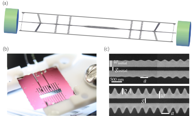
The schematic of the device is shown in Fig. S1(a). Light is coupled into and out of the device by mode-matching the output of an optical fiber to that of a terminated rectangular-shaped waveguide on both sides of the device SYHM14 . The fibers are glued permanently in etched v-grooves at optimized coupling positions. The design and fabrication of the alligator photonic crystal waveguide (PCW) are detailed in Ref. SYHM14 . The PCW is fabricated on a 200 m silicon (Si) chip coated with a 200 nm thick silicon nitride (SiN) film. The SiN device is suspended across a -mm-wide window after the silicon substrate beneath it is removed, as shown in the image of Fig. S1(b). The window allows optical access for the trapping and cooling of atoms around the device.
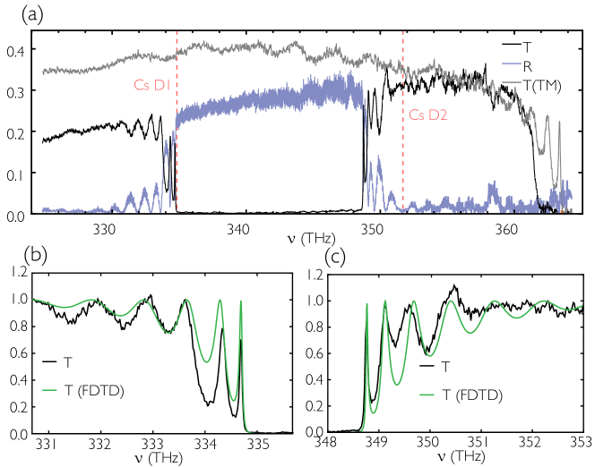
The dielectric TE mode band edge () is aligned to within GHz of the Cs D1 line ( THz) via a low-power inductively-coupled reactive-ion CF4 etch. The directional etch thins the SiN layer at a rate of 3 nm/min until a transmission measurement confirms alignment of the band edge. The final geometric dimensions of the device used in the main text are given in Fig. S1(c).
For the experiment, the chip is placed at the center of a ultra-high vacuum chamber, and the optical fibers exit through Teflon fiber feed-throughs. We measure the transmission through a device using a super luminescent diode (SLD) as the source and an optical spectrum analyzer (OSA) as the detector. The measured transmission and reflection spectra are shown in Fig. S2(a). The transmission spectra near the lower (dielectric) and upper (air) band edge are compared to an FDTD simulation in Fig. S2(b-c).
III Alligator dispersion relation from scattering images
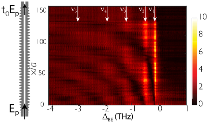
Here, we describe the analysis performed for the PCW dispersion relations in Fig. 2(e) of the manuscript. We send a single-frequency laser beam through the device and image the scattered light with a microscope. We integrate the image over the width of the PCW to produce a single plot of intensity versus position. Then we scan the laser frequency around the lower band edge to produce a 2D plot of scattered intensity as a function of position along the device and frequency of the input light.
The weak scattered light comes from small fabrication imperfections or intrinsic material defects and serves as a probe of the local intensity. Since each scatterer emits light at a different rate, we have to normalize the scattered light by a reference intensity spectrum in which the intensity of the device is known. For this reference spectrum, we average over the intensities for frequencies far from the band edge, where the PCW behaves like a waveguide, and where the local intensity in the device is approximately constant. The normalized data is shown in Fig. S3, and a zoomed-in version is in Fig. 2(a) of the manuscript.
In the FDTD simulation described above, we calculate the intensity along the center of the device for frequencies around the band edge. Taking the maximum intensity in each unit cell and normalizing by the intensity in the waveguide regime, we produce Fig. 2(b) in the main text.
Next, we fit the intensity spectrum at a given frequency to a model in order to extract the wave-vector for that frequency. Near the band edge, the field in an infinite PCW is well approximated by , where in the propagating band and inside the bandgap () The edges of a finite photonic crystal reflect with due to a large group index mismatch between the waveguide section and the photonic crystal waveguide. The resonances of the weak cavity result in the cavity-like intensity profiles seen at frequencies in Fig. S3. The intensity at a point along a finite photonic crystal of length is well approximated by a model based on the intensity in a cavity with two mirrors of reflectivity ,
| (S1) |
where is related to the overall intensity. This expression ignores the fast oscillations of the Bloch function, which go as . Note that in the bandgap (when ), the intensity model reduces to an exponential decay: . Interestingly, at the band edge (, ), the intensity displays a quadratic dependence on the position, .
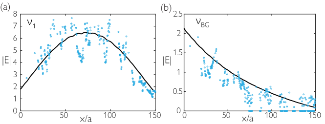
For each frequency, we fit the intensity along the nominal cells with (S1) and extract . This procedure allows us to map out the dispersion relation , which we show in Fig. 2(e) for the measured and simulated data. From the simulated fits, we find that the effective length of the cavity is cells, which is slightly longer than the nominal cells. This is expected since the cavity field can leak into the tapering sections. We use this length for the fits of the measured data. Examples of the measured and simulated intensity are shown in Fig. S4. The fluctuation of the intensity, even after the normalization, is most likely due to the spatial profile of Bloch mode. The normalization trace is taken by averaging data for excitation frequencies further away from the band-edge where the Bloch mode contrast is reduced, whereas the data closer to the band-edge has a large Bloch mode fringe visibility. However, the fluctuations do not affect the statistical fits at the level of accuracy required for the dispersion relation in our current work.
The frequency for which is defined as the band edge frequency . To extract this frequency and the curvature of the dispersion relation near the band edge, we fit the measured and simulated dispersion relations with a dispersion model SGHH15 ,
| (S2) |
where () is the lower (upper) band edge frequency, and is a frequency related to the curvature of the band near the band edge. From the measured data fits, the distance between the first resonance and band edge is GHz and THz. The simulated data give GHz and the curvature parameter is THz. These values are in good agreement with the dispersion relation from the eigenmode simulation of the infinite PCW in Fig. 1(c) of the main text, which gives THz.
IV Side-illumination trap
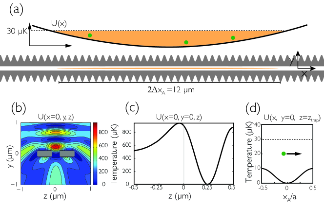
In Fig. S5(a), we show a schematic of the side-illumination (SI) trap. The side-illumination beam is nearly perpendicular to the axis of the device, has a 50 m diameter, and has a polarization aligned to the axis of the device. The orange areas represent the approximate localization of the atoms along . By time-of-flight measurements of atoms in the dipole traps, we estimate an atomic ‘temperature’ of approximately 30 K. From the beam waist and atom temperature, we can infer that the atoms are localized to m along the -axis.
Simulations of the FORT potential for the SI trap are shown in Fig. S5(b-d). The simulations are performed for the infinite structure with COMSOL. The trap depth is calibrated with the MHz AC Stark shift measured from the atomic spectra. Figure S5(b) shows the trap potential in the - plane. Atoms that are significantly hotter than K are expected to crash into the device along the diagonal directions due to Casimir-Polder forces. Figure S5(c) shows the trapping potential along the -axis. Atoms are trapped at nm. Figure S5(d) shows the trap along the -axis. Due to the photonic crystal, the trap modulates by K along the -axis, but this is significantly smaller than the estimated trap temperature.
In addition to the results in Fig. S5, we have also carried out numerical modeling of the optical trap using Lumerical simulations SLumerical of the actual finite length PCW and tapers shown in Fig. S1. We have as well included Casimir-Polder potentials as in Ref. SHung13 . More details of the trap are discussed in Ref. SGHH15 .
V Transmission model and atomic spectra fits
Here we give a more detailed description of the transmission model in the main text, which follows the derivation given in Ref. SAHC16 . A system of atoms coupled to a radiation field can be described using formalism based on the classical Green’s function SBW07 ; SDKW02 . In the Markovian limit, the field can be eliminated to obtain a master equation that describes the interactions between the atoms, . Here the Hamiltonian gives the coherent evolution of the system,
| (S3) |
and the Lindblad operator gives the dissipation of the system,
| (S4) | ||||
The Hamiltonian and Lindblad are expressed in terms of the atomic coherence operator between the ground and excited states of atom . The Hamiltonian contains terms for the free-atom evolution, the coherent atom-atom interactions, and the classical drive, respectively. is the detuning between the probe and the atomic angular frequencies. is the Rabi frequency for atom due to the guided-mode field. The atom-atom spin-exchange rate is expressed in terms of the real part of the guided mode Green’s function as
| (S5) |
where and is the dipole matrix element of atom . The Lindblad term is responsible for the dissipative interactions in the system, which include atomic decay into non-guided () and guided () modes. The decay rate into the guided mode is written in terms of the imaginary part of the Green’s function as
| (S6) |
For low atomic density along the PCW, the non-guided emission rate is not cooperative, and is described here as a single-atom effect, with as the Kronecker delta.
In the low saturation regime, the Heisenberg equations for the expectation value of the atomic coherences () can be solved for with the master equation leading to
| (S7) |
where the complex coupling rate is
| (S8) |
which is the Green’s function between atoms and projected onto the respective dipole matrix elements. In the steady-state solution, the time derivative is set to zero and result is the linear system of equations for the atomic coherences given in the main text.
The electric field in the system can be expressed in terms of the input probe field and solutions for the atomic coherences SAHC16 ,
| (S9) |
An expression for the transmission through a quasi-1D structure can be derived by solving the steady state system of equations in (S7) for the atomic coherences and substituting them into (S9). The expression can then be simplified in the case where the dipole moments are real, in which case is a complex symmetric matrix with eigenvectors and eigenvalues , and when the Green’s function is well represented by a 1D Green’s function. The final result is SAHC16 ,
| (S10) |
where is the transmission without atoms.
In the bandgap, the matrix of elements is well approximated by
| (S11) |
As discussed in the main text, when the interaction range is much larger than the separation distance (), there is only a single atomic ‘bright mode’, for which the frequency shift and guided-mode decay rate are given by and . The transmission spectra for atoms in the ‘single-bright-mode’ approximation is given by
| (S12) |
where is the detuning between the pump and the atomic frequency, and is the device transmission when no atoms are present.
Explicitly accounting for the atoms’ positions by substituting (S11) into (S12), the transmission is given by
| (S13) | ||||
We have defined in order to account for the AC-Stark shift of the atoms due to the dipole trap.
In order to accurately model the experimental conditions, we average the transmission model over atom positions and atom number. During a single measurement, the atoms are free to move along the length of the device over the range as in Fig. S5(a), evenly sampling the Bloch function. We let be an average over all positions, i.e.,
We repeat the measurement multiple times for each frequency . Each experiment can have a different number of atoms, and so we average the transmission expression over a Poisson distribution , which is a function of the average atom number . The transmission model averaged over both atom positions and atom numbers is given by
| (S14) | ||||
This is the final form of the transmission model that we use to fit the atomic spectra.
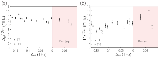
Assuming , which is obtained from the atom decay rate measurement, we fit the TE atomic spectra with (S14) and extract , , , and for each frequency. We show the values of and in Fig. 4(a) of the main text. We show the AC Stark shift and non-guided decay rate in Fig. S6.
The average of the non-guided decay rate for the TE data outside the bandgap is MHz. This is significantly larger than the expected value from the FDTD simulation, MHz. This additional inhomogeneous broadening could be due to finite temperature of the trapped atoms, vector shifts from circular light in the SI beam, atom density dependent collisional broadening, stray magnetic fields, and electric fields from charges in the dielectric. We estimate the contributions individually, and find that they likely do not explain the extraneous broadening. We note that the estimate of ‘temperature’ of trapped atoms could be improved in the future STLB08 , and it may help shed light on our excess broadening.
Interestingly, the fitted increases in the bandgap, and is as high as MHz for the last measured point. One possible explanation is that this is due to the break-down of the single bright mode approximation, as coupling to multiple collective atomic modes should result in a broadened linewidth. Another possibility is since there is a large extinction of the TE mode in the bandgap, there might be some mixing between the TE and TM modes.
We also measure transmission spectra for the TM mode, whose band edges are far-detuned from the Cs transitions. The transmission in this waveguide regime is described by an optical density model
| (S15) |
where the resonant optical density is given by . We fit the TM spectra with this model and extract , , and (assuming ). The values of and are shown with the TE data in Fig. S6. The averaged value is 0.044 , which is times smaller than for the TE mode at the first resonance , and clearly demonstrates the enhanced interaction due to the PCW.
VI Simple transmission model
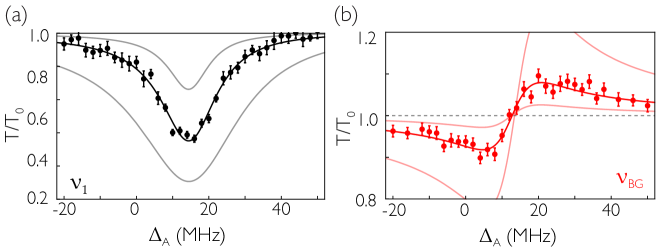
In the main text, we fit atomic transmission spectra with the averaged transmission model from (S14) in order to extract the peak guided-mode decay rate and frequency shift . In this section, we fit the spectra with a transmission model which involves no averaging, and we extract an effective decay rate and frequency shift , which will be smaller than the corresponding peak values due to the averaging of the Bloch function as the atoms move along the -axis of the trap. In the “single-bright-mode” approximation discussed in the main text, the transmission for a single collective mode with total decay rate and frequency shift is given by
| (S16) |
Here, the detuning includes the AC stark shift . Since the average number of atoms is measured independently in a decay rate measurement, the collective rates and are related to the effective rates by and . Examples of the fitted spectra for atoms outside and inside the band-gap are shown in Fig. S7. The translucent lines are the expected signals for an average atom number of and .
The fitted values of and are plotted for each detuning from the band-edge in Fig. S8(a). The results are qualitatively similar to the corresponding plot in Fig. 4(a) in the manuscript, except the effective rates and are scaled down by due to the modulation of the Bloch function . The solid line in Fig. S8(a) is the same theoretical curve as in Fig 4(a) except scaled by .
The ratio of is plotted in Fig. S8(b). Since the scale factors cancel, the result is in good agreement with the corresponding plot of in Fig. 4(b) of the manuscript. The black theory curve is the same as in the manuscript. Whereas the peak decay rate and frequency shift is sensitive to the specific model, the ratio of dissipative to coherent coupling is mostly model insensitive.

VII Atom decay measurement
We exploit the superradiance of atoms trapped near the alligator PCW to determine the mean atom number and the peak atom decay rate (at ) into the guided-modes.
As established in Ref. SGHH15 , the total exponential decay rates of the atoms is , where is the -dependent superradiance decay rate, and is the observed single-atom decay rate. We note that when , , since only the single-atom decay rate into GM and into environment remain. is numerically calculated to be MHz for cesium D1 line at the trapping site near the PCW SGHH15 .
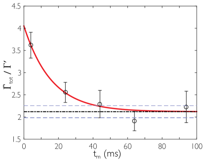
We excite the atoms with a weak resonant light pulse through the guided-mode, while the first resonance near the band edge is aligned with cesium D1 line. Pulse properties are as in Ref. SGHH15 . The subsequent fluorescence decay rates are determined through exponential fits. By varying the trap holding time after loading, the mean atom numbers for the decay measurements are varied. The decay rates are empirically fitted in an exponential form as a function of holding time SGHH15 : , as shown in Fig. S9. From the fitted asymptotic-value of the decay rates, we deduce that the apparent single-atom decay rate is .
Because the atoms are randomly distributed along direction in the trap, the observed decay curves are results after spatial averaging the coupling rates . Assuming an uniform distribution of atoms around the center of the PCW, a more detailed model specifies the form of fluorescence intensity decay as SGHH15 :
| (S17) |
where , and is the modified Bessel function. Numerically simulating the decay of single atoms in the trap by using , we compare between the exponentially fitted value and the value of used for , which yields a ratio of . This is consistent with the ratio of from measurement at long hold time ms, when single-atom decay predominates (shown as the asymptote in Fig. S9). Based on the values of deduced above, we conclude that .
At early holding times, the atom number noticeably fluctuates around some mean values . To capture this -dependent variation, we fit the decay curves by averaging with weight function of Poisson distribution probability SGHH15 . The fitting parameter here is , while we fix the value of in Eq. S17. The fit is consistent with at ms when we carry out the transmission spectra measurement. Based on the trap life time ms, we further deduce that at ms .
The linear -dependence of superradiance is given by , where is some linear coefficient, whose value is consistent with that reported in Ref. SGHH15 .
References
- (1) Goban A et al. (2015) Superradiance for atoms trapped along a photonic crystal waveguide. Phys. Rev. Lett. 115:063601.
- (2) Yu SP et al. (2014) Nanowire photonic crystal waveguides for single-atom trapping and strong light-matter interactions. App. Phys. Lett. 104:111103.
- (3) Lumerical Solutions, Inc., http://www.lumerical.com/tcad-products/fdtd/.
- (4) Hung C.-L., Meenehan SM, Chang DE, Painter O, Kimble HJ, (2013). Trapped atoms in one-dimensional photonic crystals. New J. Phys. 15: 083026.
- (5) Asenjo-Garcia A, Hood JD, Chang DE, Kimble HJ (2016) Atom-light interactions in quasi-1D dielectrics: a Green’s function perspective. http://arxiv.org/abs/1606.04977
- (6) Dung HT, Knöll L, Welsch DG (2002) Resonant dipole-dipole interaction in the presence of dispersing and absorbing surroundings. Phys. Rev. A 66:063810.
- (7) Buhmann SY, Welsch DG (2007) Dispersion forces in macroscopic quantum electrodynamics. Prog. Quantum Electron. 31:51.
- (8) Tuchendler C, Lance AM, Browaeys A, Sortais YRP, Grangier P (2008) Energy distribution and cooling of a single atom in an optical tweezer. Physical Review A 78(3):033425.