Surprising coincidence of the apparent 2D metal-to-insulator transition data with Fermi-gas based model results
Abstract
The melting condition for two-dimensional Wigner solid ( P.M. Platzman, H.Fukuyama, 1974) is shown to contain an error of a factor of . The analysis of experimental data for apparent 2D metal-to-insulator transition shows that the Wigner solidification (B.Tanatar, D.M.Ceperley, 1989) has been never achieved. Within routine Fermi gas model both the metallic and insulating behavior of different 2D system for actual range of carrier densities and temperatures is explained.
pacs:
71.27.+a, 71.30.+h, 72.10.-dRecently, much interest has been focused on the anomalous transport behavior of a wide variety of low density two-dimensional (2D) systems. It has been found that below some critical density, cooling causes an increase in resistivity, whereas in the opposite, high-density case, the resistivity decreases. The apparent metal to insulator transition was observed in n-Si MOSFET Kravchenko95 ; Pudalov99 , p-GaAsHanein98 ; Huang06 ; Huang11 ; Gao04 , n-GaAsLilly03 , n-SiGeLai05 ; Lai07 and p-SiGe Coleridge97 ; Senz99 2D systems.
I Wigner solidification vs experiment
Let us provide the rigorous analysis of the experimental data regarding Fermi gas vs Wigner solid transition. According to Ref.Platzman74 , the melting diagram of 2D Wigner solid obeys the condition , where is the coefficient assumed to be a constant at the phase transition, is the Coulomb energy associated to neighboring pair of electrons, is the 2D density. Within conventional Fermi gas model, is the average kinetic energy of single electron, where is the Fermi integral of the order of , the dimensionless temperature. Note that the average kinetic energy coincides with the thermal energy for classical Boltzmann carriers . In contrast, for degenerate electrons . In general, the solidification of strongly degenerated electrons is believed to occur at certain value of the Coulomb to Fermi energy ratio . We therefore conclude that . In Refs.Platzman74 ; Ando82 , this ratio has been erroneously defined as , thus provides wrong estimate for Wigner crystal solidification. For low-disorder 2D system Wigner solid was claimedTanatar89 to exist when .
Following Ref.Platzman74 , the phase transition can be parameterized as it follows:
| (1) |
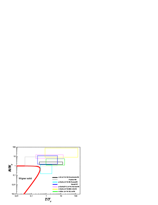
Here, the dimensional temperature and 2D density contain the valley splitting factor . Then and is the effective Borh radius and Rydberg energy respectively, is the effective mass. Note, for certain value of the correct values are lower by a factor of with respect to those predicted in Refs.Platzman74 ; Ando82 . For actual 2D systems the values are generalized in Table 1. In Fig.1 we plot the melting curvePlatzman74 specified by Eq.(1) and, moreover, the observed range of 2D densities and temperatures attributed to apparent metal-insulator transitionKravchenko95 ; Pudalov99 ; Hanein98 ; Huang06 ; Huang11 ; Gao04 ; Lilly03 ; Lai05 ; Lai07 . Evidently, Wigner solidification regime remains unaffected. Hence, we suggest the typical 2D systems can be described within routine Fermi gas model.
II Model of apparent metal-to insulator transition
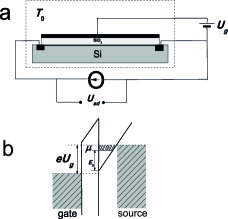
Let us first provide the arguments in favor of present use of Gibbs statistics. Since the experimental observations concern the gate-based 2D system, we represent in Fig.2 the sketch of the galvanic scheme and, moreover, the related band diagram of typical Si-MOSFET structure. The latter is assumed to operate in strong inversion regime. The applied gate voltage results in shift of Fermi level of 2D system with respect to that of the metal gate. The carrier density is given by the number of occupied states below Fermi level counted from the bottom of the lowest subband of triangular quantum well. In thermodynamic equilibrium the applied gate voltage is equal to electrostatic potential of the gate to channel capacitor, the chemical potential of 2D system and, finally, the flat-band potential . Here, is the constant difference of the work functions related to bulk silicon and metal gate respectively. The gate voltage , shifted with respect to flat-band potential yields
| (2) |
where and is the charge density and geometrical capacity of the MOS capacitor respectively. Then, and are the permittivity and thickness of the dielectric layer respectively. According to Eq.(2), the increase(decrease) of the gate voltage results in change of the chemical potential and then, in varying of 2D carrier density itself. For strongly degenerated electrons the second term in Eq.(2) can be ignored providing the apparent evidence of 2D density changed by the gate voltage. In contrast, for dilute 2D systems both terms in the right side of Eq.(2) have to be accounted. We therefore conclude that the applied gate voltage maintains the chemical potential of 2D system to be constant. Consequently, the use of Gibbs statistics for 2D system is justified.
In Ref.Cheremisin05 low-T transport in dilute 2D systems has been analyzed taking into account both the carrier degeneracy and so-called thermal correctionKirby73 owing to Peltier and Seebeck thermoelectric effects combined. For standard ohmic measurements setup, the small applied current causes heating(cooling) at the first(second) sample contact due to the Peltier effect. Under adiabatic conditions the temperature gradient is linear in current, the contact temperatures are different. The measured voltage consists of the ohmic term and, moreover, includes Peltier effect-induced thermoemf which is linear in current. According to Ref.Cheremisin05 , the total measured resistivity yields
| (3) |
where is the ohmic resistivity, is 2D thermopower, is the Lorentz number. For simplicity, we further assume that the momentum relaxation time is energy-independent. Using Gibbs statistics and parabolic energy spectrum for 2D carriers we obtain , where is the density of strongly degenerated electrons. Then, within Boltzman equation formalism the 2DEG thermopower (for 3D case, see Pisarenko, 1940) yields .
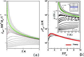
As it was demonstrated in Ref.Cheremisin05 , Eq.(3) provides the faithful sketch for transport behavior of dilute 2D systems. Both the theory results and experimental dataHanein98 are shown in Fig.3. At first, we are interested in the case of Fermi level lying above the bottom of the conducting band , which corresponds to portion of data below green line separatrix. One can distinguish the puzzling temperature behavior of the resistivity as for degenerated carriers and for high-T case . The resistivity data ( see, for example, the curve at in Fig.3) exhibits the maximum at . These values are close to those observed experimentally. The subsequent asymptotes for total resistivity specified by Eq.(3) can be written as
| (4) | |||
| (5) |
Here, is the ohmic resistivity at , is the Fermi vector, is the mean free path. Then, is the thermopower for non-generated carriers , is a correction.
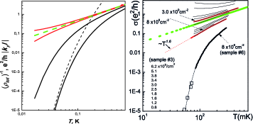
Let us examine in details the behavior of 2D resistivity shown in Fig.3. One may check whether the maxima positions of the resistivity curves obey the predicted relationship . To confirm this, in Fig.4 we plot the inverse total resistivity vs temperature and, moreover, re-plot the experimental dataHuang11 shown in Fig.3. Surprisingly, both the theory and experiment follow the expected linear dependence . Based on these findings, we suggest a simple scaling procedure which can be applied to original experimental data. Indeed, for certain resistivity curve demonstrated a certain maximum at one can find the product which is presumably universal function of ratio . The data setHanein98 scaled in this manner is represented in Fig.3b. Remarkably, the original two-order of magnitude range data shrink to roughly unique curve. In addition, we put on the same plot the result provided by theory. Indeed, for hole density cm-2 reported in Ref.Hanein98 the extrapolation yields the resistivity . The respective carrier mobility cm2/Vs corresponds to Dingle temperature K. Consequently, in Fig.3,b we plot the dimensional dependence of the product , where is the universal function. Data scaling result agrees with that provided by theory.
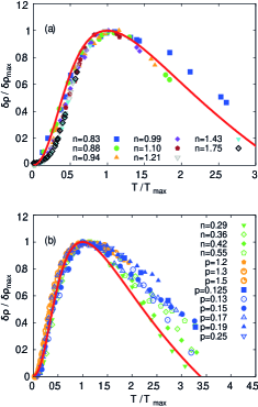
We now verify validity of our approach for different 2D systems based on scaling procedure made of use in Ref.Radonjic12 . The experimental data argued to exhibit a certain universality as function of reduced temperature and using the dimensionless form . Note that in our notations the latter ratio is equal to , thus support the universality. Fig.5 represent the scaling analysisRadonjic12 for different 2D systems. Additionally, in Fig.5 we put the result of calculations within our theory. The coincidence between theory and experiment is rather impressive.
Further progress in verifying whether our model is correct concerns the high-T dependence of the resistivity. Inverting Eq.(5) we obtain the linear dependence of inverse total resistivity as
| (6) | |||
Here, is 2D conductivity at zero temperature. High-T linear behavior of inverse total resistivity is clearly seen in experiment (see Fig.4,b) and, therefore, available for qualitative analysis with respect to theory. The estimates for temperature coefficient are summarized in Table 2 being in agreement with theory predictions. Note that zero Fermi energy case (see green lines in Fig.4) is of special interest since the inverse total resistivity vanishes at . Simultaneously, for the resistivity is expected to hyperbolic increase at clearly seen in Fig.3b, insert for p-GaAs systemHanein98 .
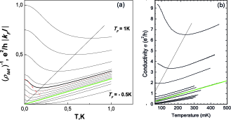
Finally, we consider the most intriguing case of Fermi level laying below the bottom of the conducting band, i.e. when . This regime corresponds to portion of data below green line seperatix in Fig.4. For actual strong insulating case the 2D density is exponentially small , while the the thermopower behavior yields the Boltzman form . Finally, we obtain the asymptote for 2D resistivity as it follows
| (7) |
In order to compare our results with experimental data, in Fig.6a we present the log-log version of Fig.4a. As expected, the curves demonstrate the progressive change from high-T linear trend to low-T activated behavior. As expected, low-T activated behavior is described by inverted Eq.(7). Surprisingly, the typical experimental resultsHuang06 shown in Fig.6b demonstrate similar behavior. Note that usually there exist an overall failureHuang06 to fit low-T data(see in Fig.6b) within variable range hopping formalism , where and corresponds to MottMott68 and Efros-ShklovskiiShklovskii84 predictions respectively.
| 2D system | , m2/Vs | ,K | (exp/th) | ref |
|---|---|---|---|---|
| Si-MOSFET | 19 | 0.38 | 2.7/0.4 | Lai07 |
| p-GaAs | 28 | 0.13 | 4.0/3.0 | Gao03 |
| p-GaAs | 32 | 0.11 | 4.7/4.5 | Huang06 ,Huang11 |
In conclusion, we demonstrate that Wigner solidification has been never achieved in experiments dealt with apparent metal to insulator transition. The observed anomalies of 2D transport behavior is explained within conventional Fermi gas formalism invoking the important correction to measured resistivity caused by Peltier and Seebeck effects combined. We represent the experimental evidence confirming the solidity and universality of the above model.
References
- (1) S.V. Kravchenko et al, Phys.Rev.B. 51, 7038, 1995
- (2) V.M. Pudalov et al, Phys.Rev.B.,60, R2154, 1999
- (3) Y. Hanein et al, Phys.Rev.Lett., 80, 1288, 1998
- (4) Jian Huang et al, Phys.Rev.B., 74, 201302(R), 2006
- (5) X.P.A. Gao et al, Phys.Rev.Lett., 93, 256402, 2004
- (6) Jian Huang et al, Phys.Rev.B., 83, 081310(R), 2011
- (7) M. P. Lilly et al, Phys.Rev.Lett., 90, 056806, 2003
- (8) K.Lai et al, Phys.Rev.B., 72, 081313(R), 2005
- (9) K.Lai et al, Phys.Rev.B., 75, 033314, 2007
- (10) P.T. Coleridge et al, Phys.Rev.B., 56, 12764(R), 1997
- (11) V. Senz et al, Ann. Phys.(Paris), 8, 237, 1999
- (12) P. M. Platzman and H. Fukuyama, Phys.Rev.B., 10, 3150, 1974
- (13) B.Tanatar and D.M.Ceperley, Phys.Rev.B., 39, 5005, 1989
- (14) T. Ando et al, Rev.Mod.Phys., 54, 437, 1982
- (15) M.V.Cheremisin, Physica E, 27, 151, 2005
- (16) C.G.M.Kirby, M.J.Laubitz, Metrologia, 9, 103, 1973
- (17) M. M. Radonjic et al, Phys.Rev.B., 85 085133, 2012
- (18) X.P.A. Gao et al, Phys.Rev.Lett., 94, 086402, 2005
- (19) X.P.A. Gao et al, Arxiv:cond-mat/0308003, 2003
- (20) N.F. Mott, J. Non-Cryst. Solids, 1, 1, 1968
- (21) B.I. Shklovskii and A.L. Efros, Electronic Properties of Doped Semiconductors, Springer-Verlag, Berlin, 1984.