Transfer matrix approach for the Kerr and Faraday rotation in layered nanostructures
Abstract
To study the optical rotation of the polarization of light incident on multilayer systems consisting of atomically thin conductors and dielectric multilayers we present a general method based on transfer matrices. The transfer matrix of the atomically thin conducting layer is obtained using the Maxwell equations. We derive expressions for the Kerr (Faraday) rotation angle and for the ellipticity of the reflected (transmitted) light as a function of the incident angle and polarization of the light. The method is demonstrated by calculating the Kerr (Faraday) angle for bilayer graphene in the quantum anomalous Hall state placed on the top of dielectric multilayers. The optical conductivity of the bilayer graphene is calculated in the framework of a four-band model.
pacs:
78.67.Wj, 72.80.Vp, 78.20.LsI Introduction
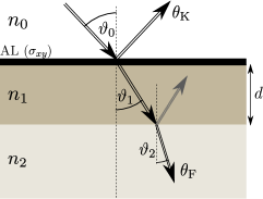
Owing to the potential applications and interesting electronic properties, atomically thin materials have attracted a strong interest in recent years. A variety of two dimensional (2D) crystals, including graphene, boron nitride, phosphorene, several transition metal dichalcogenides and complex oxides, has been prepared and studied experimentally Novoselov et al. (2005); Xu et al. (2014); Radisavljevic et al. (2011); Castellanos-Gomez et al. (2014); Gorbachev et al. (2011). Atomically thin materials are usually fabricated and studied in multi-layer structures. For example, monolayer graphene placed on a substrate can hardly be observed with optical microscopy since the intensity of the reflected light is small resulting in low contrast. However, as it was demonstrated in Refs. Novoselov et al., 2004; Nair et al., 2008, the multilayer structure shown in Fig. 1, when a dielectric spacer of width and refractive index is placed between the substrate (with refractive index ) and the graphene layer, can have important advantages. Namely, by tuning the width of the used as spacer material, the intensity of the reflected light changes drastically and consequently the visibility of the graphene flake Blake et al. (2007) is improved. Theoretically, the optical visibility of monolayer and bilayer graphene deposited on a Si/SiO2 layer substrate was also studied in Ref. Abergel et al., 2007 where it was shown that the visibility is enhanced through a resonant transmission of light due to the spacer.
Optical spectroscopies are powerful contact-free methods to study material properties. In the context of 2D materials, e.g., Zhang et al. Zhang et al. (2008) and Kuzmenko et al. Kuzmenko et al. (2009) used infrared spectroscopy to extract the tight-binding parameters in bilayer graphene by fitting the experimental reflectivity spectra with the optical conductivity calculated from the Kubo formula. If time reversal symmetry is broken, then the rotation of polarization of the transmitted (reflected) light, i.e., the Faraday (Kerr) effect can be used to deduct the off-diagonal element of the optical conductivity as was shown for monolayer graphene by Crassee et al. Crassee et al. (2011) The time reversal symmetry can be broken not only by external magnetic field, but also due to electron-electron interactions. Such an example for the latter is one of the possible gapped ground states of bilayer graphene, the so-called quantum anomalous Hall (QAH) state (for a general discussion of the possible gapped states in bilayer graphene see Ref. Zhang and MacDonald, 2012). Nandkishore and Levitov has recently proposed that this QAH state could be observed by measuring the Kerr rotation Nandkishore and Levitov (2011) in bilayer graphene samples. As an extension of Ref. Nandkishore and Levitov, 2011 the optical Hall and longitudinal conductivities of neutral bilayer graphene were calculated for four additional gapped states by Gorbar et al. Gorbar et al. (2012). The measurement of the Kerr (Faraday) angle has also been used recently to study other time reversal symmetry breaking systems, such as cuprate superconductors White and Geballe (1979); Mineev (2007); Tewari et al. (2008); Lutchyn et al. (2009) and topological insulators Valdés Aguilar et al. (2012); Jenkins et al. (2012).
According to the textbook formula White and Geballe (1979); Mineev (2007); Tewari et al. (2008); Lutchyn et al. (2009), the Kerr angle for light reflected from a conducting half space is proportional to the ac Hall conductivity of the conductor: . However, this formula is no longer valid for atomically thin materials since the thickness of the atomic layer is much thinner than the optical wavelength. For an atomic layer the relationship between the Hall conductivity and Kerr (Faraday) angle () can be derived by solving the Maxwell equations on the two sides of the atomic layer and matching solutions at the boundary. Such a derivation is presented for bilayer graphene in Ref. Nandkishore and Levitov, 2011, for thin films of topological insulators by Tse and MacDonald Tse and MacDonald (2010a, b, 2011), and for thin films of topological Weyl semimetals by Kargarian et al. Kargarian et al. (2015) Such calculations suggest that Kerr and Faraday angle measurements can also be a useful tool to characterize heterostructures fabricated recently by stacking atomically thin layers of, e.g., graphene, boron-nitride and transition metal dichalcogenides Plechinger et al. (2015); Wang et al. (2015); Withers et al. (2015a, b). This calls for a flexible and tractable theoretical framework allowing studies of magneto-optical properties of these multilayer systems.
To this end we develop a simple and versatile method to determine the Kerr and Faraday angles in multilayer systems. In our method the rotation angle and the ellipticity of the polarization for the Kerr and Faraday effect are calculated from the total transfer matrix of the multilayer structure. The total transfer matrix can always be expressed as a product of many individual transfer matrices that can be classified into two different types: i) transfer matrices corresponding to the free propagation in dielectric media, and ii) transfer matrices of atomically thin layers with given electric conductivity tensor . As we will show below this kind of classification of the possible transfer matrices makes the calculation of polarization dependent reflectivity and transmittivity simple and general. Our approach can be easily applied to different multilayer structures and for an arbitrary angle of incidence of the electromagnetic radiation. Below we also present analytical results for Kerr (Faraday) angle which makes easier the interpretation of experimental results. One of the important results of our work is that the Kerr (Faraday) angle can be enhanced by properly designing the substrate for the atomically thin materials. To demonstrate how powerful our method is we consider the multilayer setup shown in Fig. 1. The atomically thin conductor is a bilayer graphene flake placed on two layers of dielectric media of refractive indices and . Here we only consider the QAH state of bilayer graphene for which the Hall-conductivity is finite resulting in Kerr and Faraday rotation. Moreover, our method to calculate the Kerr and Faraday rotation can be applied to another exotic state called ‘All’ state proposed by Zhang et al. which breaks the chiral symmetry in bilayer graphene Zhang et al. (2011).
We note that a related approach based on the scattering matrix of the nanostructure has been used recently to study the effects of metalic surface states in topological insulator thin films Tse and MacDonald (2010a, b, 2011); Appelbaum (2014). We believe, however, that our transfer matrix method is easier to use in complex nanostructures consisting of several layers with different optical properties. Note that the transfer matrix method has been used for non-interacting graphene layers in Ref. Zhan et al., 2013 to study the transmission and reflection, but the Kerr (Faraday) effect was not considered there. Thus, our work is a generalization of Ref. Zhan et al., 2013.
The paper is organized as follows. In Sec. II, we derive the two types of transfer matrices relevant in a multilayer structure described above. Moreover, using the total transfer matrix the reflection and transmission amplitudes, Kerr and Faraday angles and the ellipticity are given. In Sec. III, we present examples for the application of our transfer matrix method, and analytical formulas for the Kerr and Faraday angles for several special cases. In order to make our work more readable the main steps of the calculation of the conductivity tensor of the gapped bilayer graphene is presented in Appendix A. In Sec. IV we make our conclusions.
II Transfer matrix method for calculating the Kerr and Faraday angles
In this section we develop a general and convenient method to calculate the Kerr and Faraday angles via the transfer matrix of layered structures consisting of stacks of dielectric materials and atomically thin conducting layers, such as graphene. In general, the total transfer matrix of such a layered structure is a product of two types of transfer matrices. The first one corresponds to a free propagation in dielectric media and we shall denote it by , the second one that gives the transfer matrix for an atomically thin material (e.g., graphene) with electric conductivity .
Regarding the geometry, we now consider an atomically thin sample on the plane embedded between dielectrics with refractive indices and at the left and right hand side of the sample, respectively as shown in Fig. 2.
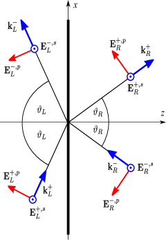
This figure shows two plane waves with wave vectors at the left hand side and two plane waves with wave vectors at the right hand side of the interface. Here the signs correspond to the direction of the propagation of the waves with respect to the axis. The electric fields of these plane waves at the left and right side of the interface are denoted by subscript and , respectively. The superscripts of these fields are further distinguished by corresponding to the polarized fields, i.e., the direction of the field is perpendicular/parallel to the plane of incidence, respectively. The transfer matrix connects the electric fields at the left hand side with that of the right hand side of the interface:
| (9) |
In what follows we present our transfer matrix method for the most general case, i.e., for the oblique incidence case. From the Maxwell equations one can derive the boundary conditions for the electric and magnetic fields and from that the transfer matrix can be extracted. Namely, from , and it follows that
| (10a) | ||||
| (10b) | ||||
where is the unit vector along the axes, is the electric field at the left/right hand side of the interface. The magnetic field of the plane wave in a dielectric is related to the electric field as . For the refractive index of a dielectric medium we take since for dielectric the relative permeability constant is . Now, from Eq. (10) we can extract the 4 by 4 transfer matrix defined in Eq. (9) and find
| (11c) | ||||
| where | ||||
| (11f) | ||||
| (11i) | ||||
| (11l) | ||||
| (11o) | ||||
| (11p) | ||||
and the angles and satisfy the Snell’s law: . Here the dimensionless conductivity is in units of and is the fine-structure constant.
One can show that the determinant of the matrix is given by
| (12) |
Note that it is independent of the conductivity .
The transfer matrix for free propagation in a dielectric medium is given by
| (13) |
where is the wave number in the dielectric, is the thickness of the dielectric medium and is the angle between the direction of the propagation and the axes. Note that .
The total transfer matrix is given by the appropriate product of the two building blocks, and . For example the total transfer matrix for the layered structure shown in Fig. 1 reads as
| (14) |
Here for brevity, we have omitted the dependence of angles and in two matrices .
The reflection amplitude and the transmission amplitude can be extracted from the total transfer matrix in the following way. Consider an incident plane wave which is a superposition of the linear and polarized light, . Now the reflection and transmission amplitudes can be represented by 2 by 2 matrices:
| (15a) | |||||
| and the reflected and the transmitted waves satisfy the following equation: | |||||
| (15f) | |||||
Hence, it is easy to obtain
| (16a) | ||||
| (16b) | ||||
| where the 4 by 4 matrix is partitioned in the same way as in Eq. (11c), i.e., | ||||
| (16e) | ||||
Note that when there is no dissipation, i.e., and then the unitarity is valid:
| (17) |
where is a 2 by 2 unit matrix. The reflectance and the transmittance for incident light are defined as
| (18a) | ||||
| (18b) | ||||
Owing to the dissipation in the atomically thin conductor, some of the incident light is absorbed, and then the absorption is given by
| (19) |
Finally, according to the textbook by Born and Wolf Born and Wolf (1999) the polarization rotation (Kerr angle) and the ellipticity for the reflected wave can be written in the form
| (20a) | ||||
| (20b) | ||||
| where | ||||
| (20c) | ||||
For Eq. (20a) implies that the Kerr angle is given by . Similar expressions are valid for the polarization rotation (Faraday angle) and the ellipticity in the case of transmitted wave, just should be replaced by in Eq. (20).
For dielectrics () our transfer matrix method gives the same results as derived, e.g., in the classical textbook by Born and Wolf Born and Wolf (1999). If the Hall conductivity is zero then no polarization rotation emerges, i.e., the Kerr and Faraday angles are zeros. Regarding single and bilayer graphene our method results in the same reflection and transmission amplitudes as used by Kuzmenko et al. Kuzmenko et al. (2009)
III Applications of the transfer matrix method
In this section using our general transfer matrix method presented in Sec. II we calculate the Kerr rotation angle for the geometrical arrangement shown in Fig. 1. To obtain simple analytical results useful for measurements we consider two special cases here: i) the atomic layer is placed directly on a substrate, i.e., the middle dielectric medium with refractive index in Fig. 1 is removed. ii) the incident light is perpendicular to the plane of the atomic layer. Since in our applications the Kerr/Faraday angle is small, i.e., we use the approximation .
To study numerically the Kerr effect we need to know the frequency dependence of the optical conductivity. As an example we take the bilayer gapped graphene and calculate its optical conductivity using our previously developed method Cserti and Dávid (2010). To make this paper self-contained, in App. A we briefly summarize the main steps to obtain the conductivity. We also compare our results with those found in Refs. Nandkishore and Levitov, 2011 and Gorbar et al., 2012 and present some numerical results for bilayer graphene in the QAH state.
III.1 Atomic layer on a thick substrate
In this case the total transfer matrix is simply where is given by Eq. (11). The Kerr angle is given by
| (21a) | ||||
| where | ||||
| (21b) | ||||
| (21c) | ||||
| (21d) | ||||
Here is the angle of the incident light, and in this subsection the superscript and the upper sign refer to polarization, while the superscript and the lower sign refer to polarization. At this point it is worth to consider a few special cases of the general formula given by Eq. (21).
i) For perpendicular incidence (, , ) the Kerr angle is given by
| (22) |
This result agrees with that derived by Nandkishore and Levitov Nandkishore and Levitov (2011), and Tse and MacDonald Tse and MacDonald (2011).
ii) For free-standing graphene (, , ) the Kerr angle reads as
| (23) |
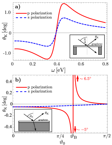
where in the last step we assumed that is approximately equal to in units of (see, e.g., Ref. Nicol and Carbotte, 2008 and our result shown in Fig. 6a) and we neglected the term proportional to in the denominator. Figure 3a shows a relatively large Kerr angle plotted as a function of frequency of the incident light for and polarization with oblique incidence.
iii) In Eq. (21a) neglecting terms in the denominator that are proportional to or we have
| (24) |
iv) Finally, the Kerr angle for polarization at the Brewster angle reads
| (25) |
where (note that now ). In the last step we neglected the term proportional to . For polarization the Kerr angle is much smaller as can be seen in Fig. 3b.
In what follows we argue that the sensitivity of the detection of the Kerr rotation can be enhanced when the incident angle is close to the Brewster angle. To see this, we calculated the frequency dependence of the optical conductivity for bilayer graphene assuming that the ground state is the QAH state. (The details of this calculation can be found in Appendix A.) Using this result we then obtained the Kerr angle as a function of the angle of incidence as shown in Fig. 3b. As it can be seen the Kerr angle is strongly enhanced for polarization when . However, using Eq. (18) one can find that at this angle the intensity of the reflected wave significantly drops down.
Thus, for an optical study of graphene or other atomically thin conducting layers the optimal incident angle should be close but not exactly equal to the Brewster angle.
III.2 Atomic layer on a substrate separated by a dielectric slab: perpendicular incidence
Here we will study the multilayer structure shown in Figure 1. The total transfer matrix is given by Eq. (14) and the Kerr angle reads
| (26a) | ||||
| (26b) | ||||
| (26c) | ||||
and is the wave number in the dielectric with refractive index and is the frequency of the incident light. Here (in contrast to Sec. III.1) the upper/lower signs are only introduced to make the expressions more compact.
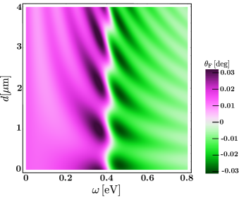
We now argue that in this setup an appropriate choice of substrate thickness makes the detection of easier in a somewhat similar way as in monolayer graphene flakes where the visibility is enhanced Plechinger et al. (2015); Wang et al. (2015). We again consider only the QAH state of bilayer graphene and calculate the dependence of the Kerr angle on the frequency and the thickness of the SiO2 dielectric. The substrate is made of Si and the electromagnetic wave incident perpendicular to the interface comes from vacuum (). The optical Hall conductivity of the bilayer graphene is calculated at zero chemical potential and temperature (see Appendix A for details). The results for Kerr angle are shown in Fig. 4.
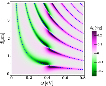
One can see from Fig. 4 that the Kerr angle is enhanced along certain lines on the plane. This is a consequence of the Fabry-Perot type resonance. Indeed, from Eq. (26) we can derive an approximate analytical expression for the resonance condition, which is given by , i.e., the first term in the denominator vanishes. Note, that the second term in the denominator is proportional to the square of the fine-structure constant and therefore it is generally a small term. Using the definitions of given by Eq. (26) the condition leads to . This equation can be satisfied in two cases:
| (27a) | ||||
| (27b) | ||||
where is an integer. For SiO2 layer (, see Ref. Malitson, 1965) and Si substrate (, see Ref. Aspnes and Studna, 1983) the above condition cannot be satisfied perfectly. Nevertheless, it is clearly seen in Fig. 4 that is strongly enhanced along lines where Eq. (27b) is approximately satisfied.
As a brief summary of our findings in Secs. III.1 and III.2 regarding the Kerr angle, the following conclusions can be drawn:
i) According to Eq. (23) the real part of the Hall conductivity for free-standing graphene can directly be determined by measuring the relatively large Kerr angle.
ii) From Eq. (III.1) it follows that the Kerr angle can be enhanced when the atomically thin material is placed on a bare substrate and the incident angle of the light is close to the Brewster angle .
iii) If the atomically thin material and the substrate are separated by a dielectric slab then owing to a Fabry-Perot type resonance the Kerr angle can be enhanced if the frequency of the incident light is tuned according to Eq. (27).
III.3 Faraday effect for atomic layer on a thick substrate
In this section we consider the same multilayer structure as in shown Fig. 1. except that the dielectric medium with refractive index is replaced by vacuum. We consider that the incident light coming from the vacuum is perpendicular to the conducting sheet. Using the theory outlined in Sec. II one can derive the following simple analytical expression for the Faraday angle .
| (28a) | ||||
| (28b) | ||||
| (28c) | ||||
and is the wave number in the dielectric with refractive index and is the frequency of the incident light. Here (in contrast to Sec. III.1) the upper/lower signs are only introduced to make the expressions more compact.
As in Sections III.1 and III.2 for our numerical calculations we take bilayer graphene in QAH state. Figure 5 shows the Faraday angle as a function of the frequency and the thickness of the substrate for perpendicular incidence.
The enhancement of the Faraday angle that can be seen in Fig. 5 is consequence of the local extrema of as a function of (see Fig. 6b in Appendix A). However, this angle is still smaller by one order of magnitude than the maximum values of the Kerr angle shown in Fig. 4. Thus, measuring the Kerr angle is more suitable than the Faraday angle to explore whether the time reversal symmetry is broken or not in bilayer graphene.
IV Conclusions
In this work we developed a general and versatile approach to calculate the rotation of the polarization of reflected and transmitted light (Kerr and Faraday effects) that is incident on multilayer systems consisting of atomically thin conducting layers and dielectrics. Introducing two kinds of transfer matrices as building blocks provides a powerful method to determine the transfer matrix of such multilayers in a simple and systematic way. From the transfer matrix we presented expressions for the intensity of the reflected and transmitted light, and the rotation angle and ellipticity of the light polarization. The expressions of these quantities are also applicable for oblique incidence of light. As an example we considered a geometrical arrangement of the multilayers as shown in Fig. 1 and for several special cases we derived analytical results for the Kerr angle. In particular, we found that if the angle of incidence is close to the Brewster angle the Kerr angle is enhanced allowing easier detection. We would like to emphasize that these analytic results can be applied to any 2D conducting materials layered with dielectrics.
In our numerical calculations the atomically thin conducting layer is taken to be a bilayer graphene using a four-band model. The measurement of the Kerr and/or Faraday rotation provides a simple optical method to determine whether the ground state is the quantum anomalous Hall state characterized by spontaneously broken time-reversal symmetry or not Nandkishore and Levitov (2011); Gorbar et al. (2012). Our newly developed transfer matrix method is an efficient procedure to design such multilayer structures in which the Kerr angle can be enhanced. As an example we showed that the Kerr angle can be maximized by tuning the thickness of the SiO2 layer.
We believe that our work for calculating the Kerr and Faraday rotations can be applied to interpret and design experiments on complex multilayers consisting of atomically thin conducting materials and dielectrics.
Acknowledgements.
We would like to thank L. Oroszlány, A. Pályi and L. Tapasztó for helpful discussions. This work is supported by the National Research, Development and Innovation Office under the contracts No. K108676.Appendix A Calculation of the optical conductivity for gapped bilayer graphene
To calculate the optical conductivity of any 2D material we applied our general method developed earlier in Ref. Cserti and Dávid, 2010. In this approach we start with an arbitrary multi band system described by a matrix Hamiltonian in a Bloch wavefunction basis: , where are the band indices (here is the number of bands of the system). Here each matrix element is a differentiable function of the wave number k corresponding to the Bloch states.
As an example we take the same four-band model of gapped bilayer graphene that is used by Gorbar et al. in Ref. Gorbar et al., 2012. This was an extension of the two-band model used by Nandkishore et al. in Ref. Nandkishore and Levitov, 2011 to describe the broken symmetry in bilayer graphene at low energy. The 4 by 4 Hamiltonian is given by
| (29) |
where , and and are valley and spin quantum numbers, respectively, while m/s is the Fermi velocity and eV is the strongest interlayer hopping. Here the most general gap reads as
| (30) |
where , , and are constants related to different gapped ground states.
The four eigenvalues of the Hamiltonian (29) are and , where
| (31) |
while and is the magnitude of the wave vector .
In general the complex optical conductivity can be calculated from the current-current correlation function using the usual analytic continuation Mahan (1990) , and it is given by
| (32) |
where and is the inverse lifetime of the particle. To calculate the current-current correlation function we applied our general method developed earlier in Ref. Cserti and Dávid, 2010 in the usual bubble approximation. To this end it is useful to write the Hamiltonian as , where are the projector operators, and and are the eigenenergies and the corresponding eigenvectors of the Hamiltonian , and in our case . The projectors satisfy the usual relation . Then the current-current correlation function with current operator (in units of which is taken into account in the expression of the conductivity) reads
| (33a) | ||||
| (33b) | ||||
where is the usual Fermi distribution and the trace is taken over the band indices. Note that to calculate the function we have used the usual summation techniques over the Matsubara’s frequencies Mahan (1990). Here we would like to emphasize that the projector operators can be calculated without knowing the eigenvectors of the Hamiltonian . Indeed, let be an hermitian matrix with distinct eigenvalues, , and then the matrix can be decomposed in terms of projector matrices as , where the projector matrix for (in the mathematical literature called Frobenius covariant Horn and Johnson (1991)) is given by
| (34) |
where is the unit matrix. The proof of (34) is based on the Cayley -Hamilton theorem Horn and Johnson (1991); Lax (2007). This theorem greatly simplifies the calculation of the current-current correlation function both analytically and numerically. Moreover, one can avoid to evaluate the spectral function of the Green’s function used for example by Nicol and Carbotte in Ref. Nicol and Carbotte, 2008.
In particular, for Hamiltonian (29) we find the correlation function for chemical potential and at zero temperature
| (35a) | ||||
| where we introduced a notation for : | ||||
| (35b) | ||||
and the integration is with respect to the polar angle of the wave vector . Since the expressions for the projectors are very lengthy we do not present them here. However, after taking the trace and performing the integration the expressions for are greatly simplified and here we list only the relevant
| (36a) | ||||
| (36b) | ||||
| (36c) | ||||
| (36d) | ||||
| (36e) | ||||
| (36f) | ||||
Now inserting Eqs. (36) into (35) we find an analytical form for the current-current correlation function at zero temperature. Then using Eqs. (32) we obtain the complex conductivity:
| (37a) | ||||
| (37b) | ||||
while and .
At this point the above form of the conductivity tensor is valid for arbitrary gap parameters , , and . From now on we take and for we use the same value as in Ref. Gorbar et al., 2012. We plotted the real and imaginary part of the complex longitudinal optical conductivity given by Eq. (37) (see Fig. 6a), and the real and imaginary part of the complex optical Hall-conductivity calculated from Eq. (37) (see Fig. 6b). Furthermore, we also compare our result with that obtained by Nandkishore and Levitov using the simplified two-band model for bilayer graphene Nandkishore and Levitov (2011) (see the gray dash-dot line in Fig. 6b).
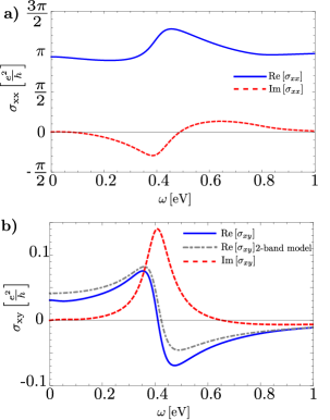
As can be seen from Fig. 6b the result from the two-band model agrees well with our four-band calculations.
Note that the current-current correlation function obtained from Eq. (35) agrees exactly with that obtained by Gorbar et al. using a different method Gorbar et al. (2012). However, the conductivity in Eq. (37) differs from that given in Ref. Gorbar et al., 2012 by a factor . As can be shown numerically this analytic difference is relevant only at low frequencies, namely for .
Note that as a check of our calculation of the optical conductivity it can be shown that
| (38) |
when the spin and valley degeneracy are taken into account.
References
- Novoselov et al. (2005) K. S. Novoselov, D. Jiang, F. Schedin, T. J. Booth, V. V. Khotkevich, S. V. Morozov, and A. K. Geim, PNAS 102, 10451 (2005).
- Castellanos-Gomez et al. (2014) A. Castellanos-Gomez, L. Vicarelli, E. Prada, J. O. Island, K. L. Narasimha-Acharya, S. I. Blanter, D. J. Groenendijk, M. Buscema, G. A. Steele, J. V. Alvarez, H. W. Zandbergen, J. J. Palacios, and H. S. J. van der Zant, 2D Materials 1, 025001 (2014).
- Xu et al. (2014) X. Xu, W. Yao, D. Xiao, and T. F. Heinz, Nat Phys 10, 343 (2014).
- Gorbachev et al. (2011) R. V. Gorbachev, I. Riaz, R. R. Nair, R. Jalil, L. Britnell, B. D. Belle, E. W. Hill, K. S. Novoselov, K. Watanabe, T. Taniguchi, A. K. Geim, and P. Blake, Small 7, 465 (2011).
- Radisavljevic et al. (2011) B. Radisavljevic, A. Radenovic, J. Brivio, V. Giacometti, and K. A., Nat Nano 6, 147 (2011).
- Novoselov et al. (2004) K. Novoselov, A. Geim, S. Morozov, D. Jiang, Y. Zhang, S. Dubonos, I. Grigorieva, and A. Firsov, Science 306, 666 (2004).
- Nair et al. (2008) R. R. Nair, P. Blake, A. N. Grigorenko, K. S. Novoselov, T. J. Booth, T. Stauber, N. M. R. Peres, and A. K. Geim, Science 320, 1308 (2008).
- Blake et al. (2007) P. Blake, E. W. Hill, A. H. Castro Neto, K. S. Novoselov, D. Jiang, R. Yang, T. J. Booth, and A. K. Geim, Appl. Phys. Lett. 91, 063124 (2007).
- Abergel et al. (2007) D. S. L. Abergel, A. Russell, and V. I. Fal’ko, Appl. Phys. Lett. 91, 063125 (2007).
- Zhang et al. (2008) L. M. Zhang, Z. Q. Li, D. N. Basov, M. M. Fogler, Z. Hao, and M. C. Martin, Phys. Rev. B 78, 235408 (2008).
- Kuzmenko et al. (2009) A. B. Kuzmenko, I. Crassee, D. van der Marel, P. Blake, and K. S. Novoselov, Phys. Rev. B 80, 165406 (2009).
- Crassee et al. (2011) I. Crassee, J. Levallois, A. L. Walter, M. Ostler, A. Bostwick, E. Rotenberg, T. Seyller, D. van der Marel, and A. B. Kuzmenko, Nat Phys 7, 48 (2011).
- Zhang and MacDonald (2012) F. Zhang and A. H. MacDonald, Phys. Rev. Lett. 108, 186804 (2012).
- Nandkishore and Levitov (2011) R. Nandkishore and L. Levitov, Phys. Rev. Lett. 107, 097402 (2011).
- Gorbar et al. (2012) E. V. Gorbar, V. P. Gusynin, A. B. Kuzmenko, and S. G. Sharapov, Phys. Rev. B 86, 075414 (2012).
- White and Geballe (1979) R. M. White and T. Geballe, Long Range Order in Solids (Academic Press, New York, 1979).
- Mineev (2007) V. P. Mineev, Phys. Rev. B 76, 212501 (2007).
- Tewari et al. (2008) S. Tewari, C. Zhang, V. M. Yakovenko, and S. Das Sarma, Phys. Rev. Lett. 100, 217004 (2008).
- Lutchyn et al. (2009) R. M. Lutchyn, P. Nagornykh, and V. M. Yakovenko, Phys. Rev. B 80, 104508 (2009).
- Valdés Aguilar et al. (2012) R. Valdés Aguilar, A. V. Stier, W. Liu, L. S. Bilbro, D. K. George, N. Bansal, L. Wu, J. Cerne, A. G. Markelz, S. Oh, and N. P. Armitage, Phys. Rev. Lett. 108, 087403 (2012).
- Jenkins et al. (2012) G. S. Jenkins, A. B. Sushkov, D. C. Schmadel, M.-H. Kim, M. Brahlek, N. Bansal, S. Oh, and H. D. Drew, Phys. Rev. B 86, 235133 (2012).
- Tse and MacDonald (2010a) W.-K. Tse and A. H. MacDonald, Phys. Rev. Lett. 105, 057401 (2010a).
- Tse and MacDonald (2010b) W.-K. Tse and A. H. MacDonald, Phys. Rev. B 82, 161104 (2010b).
- Tse and MacDonald (2011) W.-K. Tse and A. H. MacDonald, Phys. Rev. B 84, 205327 (2011).
- Kargarian et al. (2015) M. Kargarian, M. Randeria, and N. Trivedi, Sci. Rep. 5, 12683 (2015).
- Plechinger et al. (2015) G. Plechinger, F. Mooshammer, A. Castellanos-Gomez, G. A. Steele, C. Schüller, and T. Korn, 2D Materials 2, 034016 (2015).
- Wang et al. (2015) Z. Wang, D.-K. Ki, H. Chen, H. Berger, A. H. MacDonald, and A. F. Morpurgo, Nat Commun 6 (2015).
- Withers et al. (2015a) F. Withers, O. Del Pozo-Zamudio, A. Mishchenko, A. P. Rooney, A. Gholinia, K. Watanabe, T. Taniguchi, S. J. Haigh, A. K. Geim, A. I. Tartakovskii, and K. S. Novoselov, Nat Mater 14, 301 (2015a).
- Withers et al. (2015b) F. Withers, O. D. Pozo-Zamudio, S. Schwarz, S. Dufferwiel, P. M. Walker, T. Godde, A. P. Rooney, A. Gholinia, C. R. Woods, P. Blake, S. J. Haigh, K. Watanabe, T. Taniguchi, I. L. Aleiner, A. K. Geim, V. I. Fal’ko, A. I. Tartakovskii, and K. S. Novoselov, Nano Letters 15, 8223 (2015b).
- Zhang et al. (2011) F. Zhang, J. Jung, G. A. Fiete, Q. Niu, and A. H. MacDonald, Phys. Rev. Lett. 106, 156801 (2011).
- Appelbaum (2014) I. Appelbaum, J. Appl. Phys. 116, 064903 (2014).
- Zhan et al. (2013) T. Zhan, X. Shi, Y. Dai, X. Liu, and J. Zi, J. Phys.: Condens. Matter 25, 215301 (2013).
- Born and Wolf (1999) M. Born and E. Wolf, Principles of optics, seventh ed. (Cambridge University Press, Cambridge, UK, 1999).
- Cserti and Dávid (2010) J. Cserti and G. Dávid, Phys. Rev. B 82, 201405 (R) (2010).
- Nicol and Carbotte (2008) E. J. Nicol and J. P. Carbotte, Phys. Rev. B 77, 155409 (2008).
- Malitson (1965) I. H. Malitson, J. Opt. Soc. Am. 55, 1205 (1965).
- Aspnes and Studna (1983) D. E. Aspnes and A. A. Studna, Phys. Rev. B 27, 985 (1983).
- Mahan (1990) G. D. Mahan, Many-Particle Physics (Plenum Press, 2nd ed., New York and London, 1990).
- Horn and Johnson (1991) R. A. Horn and C. R. Johnson, Topics in Matrix Analysis (Cambridge University Press, Cambridge, UK, 1991).
- Lax (2007) P. D. Lax, Linear Algebra and Its Applications (John Wiley and Sons Inc., 2nd ed., New York, United States, 2007).