Quantized conductance doubling and hard gap in a two-dimensional semiconductor-superconductor heterostructure
Coupling a two-dimensional (2D) semiconductor heterostructure to a superconductor opens new research and technology opportunities, including fundamental problems in mesoscopic superconductivity, scalable superconducting electronics, and new topological states of matter. One route towards topological matter is by coupling a 2D electron gas with strong spin-orbit interaction to an s-wave superconductor. Previous efforts along these lines have been adversely affected by interface disorder and unstable gating. Here we show measurements on a gateable InGaAs/InAs 2DEG with patterned epitaxial Al, yielding devices with atomically pristine interfaces between semiconductor and superconductor. Using surface gates to form a quantum point contact (QPC), we find a hard superconducting gap in the tunneling regime. When the QPC is in the open regime, we observe a first conductance plateau at , consistent with theory. The hard-gap semiconductor-superconductor system demonstrated here is amenable to top-down processing and provides a new avenue towards low-dissipation electronics and topological quantum systems.
Introduction—Recent work on semiconductor nanowires has offered evidence for the existence of Majorana zero modes, a signature of the topological superconductivity Mourik:2012je ; Das:2012hi ; Deng:2012gn . A characteristic of the first studies in this area was significant subgap tunneling conductance (a so-called soft gap), attributed to disorder at the semiconductor-superconductor (Sm-S) interface Takei:2013id ; Cole:2015bl . In nanowires, the soft-gap problem was recently resolved by growing Al epitaxially on InAs nanowires, yielding greatly reduced subgap conductance Chang:2015kw ; Higginbotham:2015ii . Studies of Sm-S systems based on top-down processed gateable two-dimensional electron gases (2DEGs) coupled to superconductors have not explicitly addressed the soft-gap issue yet Amado2013 ; Irie2014 . However experiments on such systems have demonstrated other theoretical predictions, such as quantization of critical current Irie2014 ; Takayanagi:1995hg ; Bauch:2005gh , the retro-reflection property of Andreev scattering Jakob:2000cw , and spectroscopy of a gate-defined quantum dot with superconducting leads Deon2011 ; Deon2011_2 , which do not require a hard proximity-induced gap in the semiconductor.
The two main results we present in this paper are both consequences of the transparent epitaxial Sm-S interface and overcome the soft gap problem for 2D electron gases. The first is a doubling of the the lowest quantized conductance plateau, from in the normal state to in the superconducting state, as predicted theoretically Beenakker:1992dd . The second is a strong suppression of conductance for voltages smaller than the superconducting gap when the QPC is in the tunneling regime—that is, the detection of a hard superconducting gap in a proximitized 2DEG. Conductance doubling arises from Andreev reflection transferring charge into the superconductor Andreev:1964uy . The hard gap reflects the absence of electronic states below the superconducting gap in the semiconductor. Using gate voltage to control the QPC, we measure conductance across the transition from weak tunneling to the open-channel regime and find good (but not perfect) agreement with the theory of a normal-QPC-superconductor structure Beenakker:1992dd .
Results
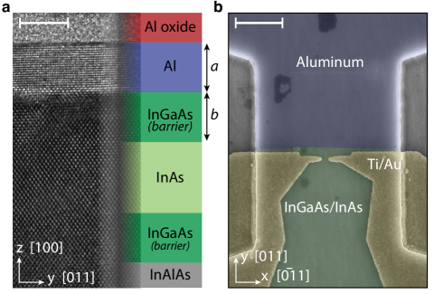
Properties of the 2DEG and the superconducting Al film—The starting material is an undoped InAs/InGaAs heterostructure with epitaxial Al as a top layer, grown by molecular beam epitaxy Javad:Xwv0duEK . A cross-sectional TEM showing a sharp epitaxial Sm-S interface is shown in Fig. 1a. In the devices reported here, the thickness of the InGaAs barrier was nm, and the Al film was nm. A Hall ball fabricated on the same wafer with the Al removed (see Methods) gave density cm-2 and mobility cm, yielding a mean free path . In a similar wafer, weak anti-localization analysis gave a spin-orbit length Javad:Xwv0duEK . The Al film has a critical temperature K, corresponding to a gap , enhanced from the bulk value of Al, and consistent with other measurements on Al films of similar thickness Chubov:1969uu . The in-plane critical field of the Al film is T Javad:Xwv0duEK .
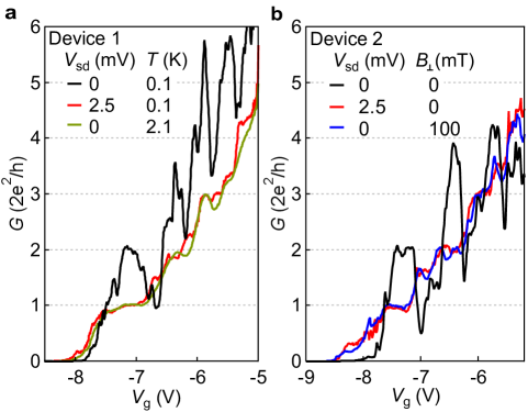
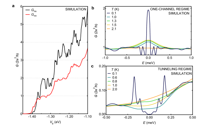
Quantized conductance doubling—A scanning electron micrograph of Device 1 is shown in Fig. 1b.The conductance of the QPC is tuned by negative voltages applied to the gates. The QPC is located in front of the region where the Al film has not been removed. Figure 2 shows conductance traces for the two lithographically similar QPCs. In the superconducting state, both devices show increased conductance at the plateau of the QPC and suppressed conductance below , where , relative to the normal state. This behavior is the hallmark of Andreev reflection being the dominant conduction mechanism through the QPC Beenakker:1992dd ; Mortensen:1999gw . Raising the temperature above the critical temperature of the Al film, applying an out-of-plane magnetic field, or applying a bias larger than the gap, all bring the lowest plateau back to (see Fig. 2). The dip structure at the transition between conductance plateaus was also observed in a similar experiment on nanowires Zhang:2016vl , and is presumably caused by mode mixing due to disorder, leading to a reduction in transparency of the already open first channel. A constant contact resistance k has been subtracted in each viewgraph, a value chosen to move the first plateau in the normal state to .
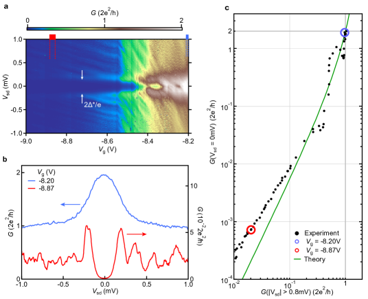
Hard superconducting gap—By further depleting the electron gas in the constriction, the device is operated as a tunnel probe of the local density of states in the InAs 2DEG. This technique has been applied to studying subgap properties of semiconductor nanowires coupled to superconductors Mourik:2012je ; Deng:2012gn ; Das:2012hi ; Churchill:2013cq ; Lee:2014gj ; Chang:2015kw . In Fig. 3a the QPC voltage is decreased to gradually transition from the one-channel regime, where the zero bias conductance is , to the tunneling regime, where conductance is strongly suppressed for . From these measurements, the gap in the density of states of the InAs due to the proximity to the Al is estimated to be (measured peak-to-peak). The value of is similar, but not identical, to the gap in the Al film as estimated from , as discussed above.
In the case of perfect Andreev reflection from the superconductor/semiconductor interface, the conductance of one channel through a constriction proximal to the interface is given by
| (1) |
where is the conductance when the film is superconducting, and is the conductance in the normal state Beenakker:1992dd . In Fig. 3c the prediction in Eq. (1) with no free parameters (green line) and experimental data are shown. Here, is the average conductance for , justified by the equality of applying a bias and raising the temperature above , as shown in Fig. 2a. Equation (1) is consistent with the data over two orders of magnitude in , indicating that the zero bias conductance up to is well described by the prediction of perfect Andreev reflection of a single QPC mode. Equation (1) represents the only quantitative theory of the relation between subgap conductance and normal state conductance (i.e. the hard gap) of which we are aware, and the agreement between Eq. (1) and the experiment in Fig. 3c leads to the designation of a hard gap in this superconductor-2DEG system. However, the systematic deviation between data and prediction in Fig. 3c for could be a manifestation of a small remnant non–zero normal scattering probability.
The shapes of the conductance curves at in the tunneling regime (red line in Fig. 3b) are smeared relative to the conventional Bardeen-Cooper-Schrieffer (BCS) density of states of a superconductor. This could be due to broadening of the BCS coherence peaks in the disordered superconducting film formed in the 2DEG under the Al Feigelman:2012fp , a weak coupling between Al and 2DEG Cole:2015bl or the layout of the tunnel probe relative to the proximitized 2DEG Gueron:1996hw ; leSueur:2008kl ; Cherkez:2014jz .
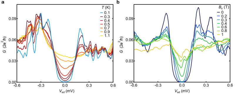
Temperature dependence of the density of states—The temperature dependence of the conductance in the Andreev QPC is different in the one-channel and in the tunnel regime (Fig. 4). The one-channel regime (Fig. 4a,b) has a pronounced kink at , presumably associated with the sudden onset of Andreev enhanced subgap conductance. In contrast, the temperature-dependence in the tunnel regime (Fig. 4c,d) is smeared close to due to thermally excited quasiparticles.
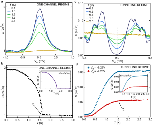
The temperature dependence is simulated (insets in Fig. 4) by calculating where is the Fermi function which accounts for thermal broadening. The conductance is calculated by combining scattering matrices of quasielectrons and quasiholes in the normal region and Andreev reflection at the superconductor interface (details of the simulation is given in methods). The scattering matrices are calculated using the numerical package Kwant Groth:2014ia , and the simulation is performed using the device geometry from the micrograph in Fig. 1b. The temperature dependence of the gap is modeled with , and the Andreev reflection amplitude is taken from Beenakker:1992dd . The simulation shows good quantitative agreement with the data.
Magnetic field dependence of the density of states—To drive a superconductor/semiconductor device into a topological regime, one requirement is , while the native superconductor retains its gap. Figure 5 shows the in-plane magnetic field dependence of , from which an approximate critical field mT is extracted. A rough estimate of the -factor can be inferred by assuming the critical results from Zeeman energy surpassing the induced superconducting gap, that is , which yields , similar to the -factor in bulk InAs. In Fig. 5d the zero-bias conductance is shown for the two different in-plane directions, and the slight direction dependence of could be due to an anisotropic -factor in the InAs crystal lattice. The induced gap in the 2DEG disappears at in plane magnetic fields significantly smaller than the critical field of the Al film itself. The 2DEG has a strong spin-orbit interaction (), which, taken together with the intimate coupling to the superconductor, makes this material system a feasible candidate to realize topological superconducting devices. By using top-down fabrication techniques and the electrostatic gating demonstrated here, effective 1D systems can be produced, in which an in-plane magnetic field can close the induced superconducting gap to reach a topological phase.
In conclusion, we observe quantization doubling through a QPC proximal to a superconductor/semiconductor interface, confirming a long-standing theoretical prediction Beenakker:1992dd . Operated as a gate-tunable tunnel probe of the local density of states, the QPC shows a hard superconducting gap induced in the 2DEG. The magnetic field dependence of the induced gap compares favorably with the critical field of the superconducting film, opening possibilities to pursue topological states of matter in one-dimensional structures fabricated from epitaxial Al/2D InAs material.
Methods
Fabrication and measurement setup—Ohmic contacts to the InAs electron gas are formed by the epitaxial Al directly and mesa structures are patterned by standard III-V chemical etching techniques. The aluminum is etched using commercial Transene Aluminum Etch D. Subsequent to the selective Al etch, an insulating 40 nm Al2O3 layer is deposited using atomic layer deposition and metallic gates (5 nm Ti/50 nm Au) are evaporated onto the device. The measurements were performed in a dilution refrigerator with a base mixing chamber temperature mK, using four-terminal lock-in techniques and DC measurements.
Measurement details—The data in Fig. 3 is measured in a DC setup, incrementing the voltage in steps of size V. The data is smoothed over 10 steps and the derivative is calculated numerically to obtain the differential conductance. A constant contact resistance is subtracted from the data, moving the conductance at V for mV to . The 4-terminal resistance of the device is = 400 with V. The difference between and is most likely dominated by the change of resistivity near the gated region, when the gate is turned on, as well as the distance from the voltage probe to the QPC region. The voltage probes are located m away from the QPC and the gates overlap the mesa over an area m2. The normal state conductance is calculated as the average of for in the range . The analysis is largely unaffected by changing the averaging window for values mV. The cuts in Fig. 3b are taken by averaging over a 12 mV (30 mV) window in for the one-channel (tunneling) regime. Finally, each datapoint in Fig. 3c is calculated as the average over a mV range in .
Model for numerical simulations—We calculate the conductance of the junction in two steps. Firstly, we determine the scattering properties of the normal region which we assume is a 1.1 m wide channel of length , where we have taken dimensions from SEM in Fig. 1b. It is described by the spinless Hamiltonian,
| (2) |
We model the QPC as two rectangular gates located at nm, with the width , separated by the length and located at the distance above 2DEG (see Supplementary Fig. 3 for illustration of and ). We calculate the potential generated by the QPC electrodes, , for the gate voltage following davies_modeling_1995 , with
| (3) |
where
| (4) |
and . The potential landscape of the simulation is shown in Supplementary Fig. 3.
We include disorder ando_quantum_1991 by adding a random on-site energy distributed uniformly between and where
| (5) |
Due to limitation of the computational mesh resolution we exclude the disorder from the vicinity of the QPC and take only for nm.
We calculate the scattering matrix of the normal part of the junction for a quasiparticle at the energy as
| (6) |
using Kwant package Groth:2014ia and discretizing the Hamiltonian in Eq. (2) on a mesh with the spacing nm. The quantities and denote reflection and transmission submatrices for a time-reversal symmetric system. In the second step, we combine the scattering matrices calculated for and (that correspond to quasielectron and quasihole respectively) with the matrix that accounts for the Andreev reflection at the superconductor interface
| (7) |
where
| (8) |
The latter equation describes the Andreev reflection amplitude Beenakker:1992dd including the temperature dependent pairing potential . Finally we calculate the conductance according to
| (9) |
where stands for the Fermi function
| (10) |
and where . is the number of modes in the normal lead. The quasielectron and quasihole reflection matrices are given by:
| (11) |
| (12) |
Additionally, the normal-state conductance is given by . Results of the simulations are shown Supplementary Figures 3, 4 and 5.
Data and code availability statement—All data presented in the main paper and supplement, as well as code used to generate simulations are available from the authors upon request.
Acknowledgements: Research support by Microsoft Project Q, the Danish National Research Foundation. C.M.M. acknowledges support from the Villum Foundation. F.N. acknowledges support from a Marie Curie Fellowship (No. 659653). M.P.N. acknowledges support from ERC Synergy Grant. A.A. is supported by an ERC Starting Grant. M.W. and A.A. are supported by the Foundation for Fundamental Research on Matter (FOM) and the Netherlands Organization for Scientific Research (NWO/OCW) as part of the Frontiers of Nanoscience program. We are indebted to S. Kraemer for the TEM analysis, performed at the UCSB MRL Shared Experimental Facilities (NSF DMR 1121053), a member of the NSF-funded Materials Research Facilities Network.
Authors Contribution: M.K., F.N., H.J.S. and C.M. conceived the experiment. M.K., F.N., H.J.S. designed, fabricated and measured the devices and wrote the manuscript, with comments from all other authors. J.A.F. and K.F. provided input on interpretations. M.P.N, M.W and A.R.A. developed theory and code for the simulations. The wafer was grown by J.S. and C.J.P.
Competing interests: The authors declare no competing interests.
References
- (1) Mourik, V. et al. Signatures of Majorana Fermions in Hybrid Superconductor-Semiconductor Nanowire Devices. Science 336, 1003–1007 (2012).
- (2) Das, A. et al. Zero-bias peaks and splitting in an Al-InAs nanowire topological superconductor as a signature of Majorana fermions. Nature Physics 8, 887–895 (2012).
- (3) Deng, M. T. et al. Anomalous Zero-Bias Conductance Peak in a Nb–InSb Nanowire–Nb Hybrid Device. Nano Letters 12, 6414–6419 (2012).
- (4) Takei, S., Fregoso, B. M., Hui, H.-Y., Lobos, A. M. & Das Sarma, S. Soft Superconducting Gap in Semiconductor Majorana Nanowires. Physical Review Letters 110, 186803 (2013).
- (5) Cole, W. S., Das Sarma, S. & Stanescu, T. D. Effects of large induced superconducting gap on semiconductor Majorana nanowires. Physical Review B 92, 174511 (2015).
- (6) Chang, W. et al. Hard gap in epitaxial semiconductor–superconductor nanowires. Nature Nanotechnology 10, 232–236 (2015).
- (7) Higginbotham, A. P. et al. Parity lifetime of bound states in a proximitized semiconductor nanowire. Nature Physics 11, 1017–1021 (2015).
- (8) Amado, M. et al. Electrostatic tailoring of magnetic interference in quantum point contact ballistic Josephson junctions. Physical Review B 87, 134506 (2013).
- (9) Irie, H., Harada, Y., Sugiyama, H. & Akazaki, T. Josephson coupling through one-dimensional ballistic channel in semiconductor-superconductor hybrid quantum point contacts. Physical Review B 89, 165415 (2014).
- (10) Takayanagi, H., Akazaki, T. & Nitta, J. Observation of Maximum Supercurrent Quantization in a Superconducting Quantum Point-Contact. Physical Review Letters 75, 3533–3536 (1995).
- (11) Bauch, T. et al. Correlated quantization of supercurrent and conductance in a superconducting quantum point contact. Physical Review B 71, 174502 (2005).
- (12) Jakob, M. et al. Direct determination of the Andreev reflection probability by means of point contact spectroscopy. Applied Physics Letters 76, 1152–1154 (2000).
- (13) Deon, F. et al. Quantum dot spectroscopy of proximity-induced superconductivity in a two-dimensional electron gas. Applied Physics Letters 98, 132101 (2011).
- (14) Deon, F. et al. Proximity effect in a two-dimensional electron gas probed with a lateral quantum dot. Physical Review B 84, 100506 (2011).
- (15) Beenakker, C. W. J. Quantum transport in semiconductor-superconductor microjunctions. Physical Review B 46, 12841–12844 (1992).
- (16) Andreev, A. F. The Thermal Conductivity of the Intermediate State in Superconductors. Soviet Physics Jetp-Ussr 19, 1228–1231 (1964).
- (17) Shabani, J. et al. Two-dimensional epitaxial superconductor-semiconductor heterostructures: A platform for topological superconducting networks. Physical Review B 93, 155402 (2016).
- (18) Chubov, P. N., Eremenko, V. V. & Pilipenkko, Y. A. Dependence of the critical temperature and energy gap on the thickness of superconducting aluminum films. JETP Letters 28, 389–395 (1969).
- (19) Mortensen, N. A., Jauho, A.-P., Flensberg, K. & Schomerus, H. Conductance enhancement in quantum-point-contact semiconductor-superconductor devices. Physical Review B 60, 13762–13769 (1999).
- (20) Zhang, H. et al. Ballistic Majorana nanowire devices. Preprint at http://arxiv.org/abs/1603.04069 (2016).
- (21) Churchill, H. O. H. et al. Superconductor-nanowire devices from tunneling to the multichannel regime: Zero-bias oscillations and magnetoconductance crossover. Physical Review B 87, 241401 (2013).
- (22) Lee, E. J. H. et al. Spin-resolved Andreev levels and parity crossings in hybrid superconductor-semiconductor nanostructures. Nature Nanotechnology 9, 79–84 (2014).
- (23) Feigel’man, M. V. & Skvortsov, M. A. Universal Broadening of the Bardeen-Cooper-Schrieffer Coherence Peak of Disordered Superconducting Films. Physical Review Letters 109, 147002 (2012).
- (24) Guéron, S., Pothier, H., Birge, N. O., Esteve, D. & Devoret, M. H. Superconducting Proximity Effect Probed on a Mesoscopic Length Scale. Physical Review Letters 77, 3025–3028 (1996).
- (25) le Sueur, H., Joyez, P., Pothier, H., Urbina, C. & Esteve, D. Phase Controlled Superconducting Proximity Effect Probed by Tunneling Spectroscopy. Physical Review Letters 100, 197002 (2008).
- (26) Cherkez, V. et al. Proximity Effect between Two Superconductors Spatially Resolved by Scanning Tunneling Spectroscopy. Physical Review X 4, 011033 (2014).
- (27) Groth, C. W., Wimmer, M., Akhmerov, A. R. & Waintal, X. Kwant: a software package for quantum transport. New Journal of Physics 16, 063065 (2014).
- (28) Davies, J. H., Larkin, I. A. & Sukhorukov, E. V. Modeling the patterned two‐dimensional electron gas: Electrostatics. Journal of Applied Physics 77, 4504–4512 (1995).
- (29) Ando, T. Quantum point contacts in magnetic fields. Phys. Rev. B 44, 8017–8027 (1991).
Supplementary material for “Quantized conductance doubling and hard gap in a two-dimensional semiconductor-superconductor heterostructure”
Appendix A Supplementary note 1: Measurements on alternate wafer
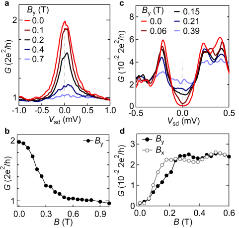
Under identical growth conditions, a wafer without an InGaAs top barrier (i.e. nm) between the epitaxial aluminum and the InAs quantum well was produced. The density and mobility, measured using a conventional Hall bar geometry, was m-2 and cmVs, corresponding to a mean free path of nm. In a lithographically similar device to that shown in Fig. 1 of the main text, we observe a hard superconducting gap (Supplementary Figure S1). When the gates are operated in the quantum point contact regime, we did not observe quantized steps in conductance. The non-monotonic decrease in conductance at mV, believed to be due to disorder in the 2DEG, makes the identification of a superconducting gap in this wafer difficult (Supplementary Fig. S1b).
However, by increasing the temperature (Supplementary Fig. S2a) or the magnetic field (Supplementary Fig. S2b) we confirm that the gap in the density of states in Supplementary Fig. S1 is related to the superconducting properties, and not a spurious quantum dot.
A.1 Supplementary Note 2: Numerical results
The potential landscape generated by the simulation, used to model the QPC is shown in Supplementary Figure 3.
For the simulation we adopt the following parameters: chemical potential meV, mean free path nm, effective mass (obtained from calculation of the Fermi velocity for a single mode quantum well in the growth direction). We also assume K and eV. The QPC geometry is set by the parameters: nm (width of gates), nm (separation between gates) and nm (distance from gates down to the 2DEG).
We consider a system of the geometry similar to the one presented on Fig. 1b of the main text. Here the superconductor interface is located 230 nm after the QPC.
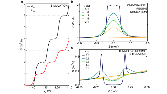
Supplementary Figure S4a shows the conductance as a function of the gate voltage. The conductance depicted with the black curve is quantized in multiplies of as the transport involves transmission of an electron and an Andreev-reflected hole. Supplementary Figures S4b,c show the Andreev-enhanced spectroscopy curves obtained by varying the injection energy . Supplementary Figures S4b and S4b show, respectively, the calculated finite–bias properties of the one–channel regime and the tunneling regime, for several values of the temperature. The value of in the simulations are chosen so the conductance at zero bias match the data at in Fig. 4 of the main text. The low temperature spectroscopy curves are similar the ones obtained by using the analytic expression of Blonder-Tinkham-Klapwijk (BTK) blonder_transition_1982 . However, for energies larger than the gap, the spectroscopy simulations show an increasing trend as a function of (cf. the orange curves on Supplementary Fig. S4b,c where ), due to an increase of the energy of the injected particle with respect to the QPC potential. This dependence is pronounced in our geometry, because the slopes of the QPC steps are less than meV wide, making the conductance sensitive to changes in on the scale of single meV.
The low temperature one-channel spectroscopy curve shows maxima at (blue curve in Supplementary Fig. S4b) while in the experimental data (cf. Fig. 4a and Fig. 5a of the main text) the curves decrease smoothly as is increased. Previous theoretical work hekking_subgap_1994 showed that the detailed layout of the interface between the normal and superconducting electrodes (at the scale of the coherence length) impacts the subgap conductance due to interference between two electrons tunneling through the interface. Moreover, smearing of the superconducting coherence peak feigelman_universal_2012 is predicted to be an effect of disorder present in the superconducting film pointing again to the role of normal-superconductor interface.
The experimental structure consist of an extended 2DEG/superconductor interface created by the InGaAs/InAs heterostructure covered by Al. In the present calculations, we are limited to an abrupt semiconductor/superconductor interface. We therefore also consider a case where the distance from the QPC to the interface is increased relative to the lithographic dimensions.
Supplementary Figure S5 shows results obtained for a system with 800 nm distance between the QPC gates and the superconductor interface. In this calculation the scattering region is longer than the mean free path, leading to the peak/dip structures superimposed on the QPC conductance steps. Similar peaks/dips are observed in the experimental data in Figs. 2a,b of the main text. The fluctuations are more pronounced in the superconducting case () due to the Andreev-enhanced conductance involving traversing the scattering region twice. The resonant features are also visible in the low temperature spectroscopy curves for energies larger the superconducting gap (cf. Supplementary Figs. S5b,c), similar to the experimental curves in Figs. 4 a,c of the main text. Comparable pinch off curves are obtained when the disorder is located before the QPC, if the distance between the QPC and the superconductor are short.
The most notable feature of the system with extended length between the QPC and the superconductor is a significant reduction of the width of the central peak in the one–channel finite–bias simulations (blue curve in Supplementary Fig. S5b). The rapid drop in conductance is a hallmark of an induced gap, for which the chaotic billiard in the region between the QPC gates and superconductor has zero density of states. The energy scale at which conductance drops is denoted , and has the magnitude of Thouless energy melsen_induced_1996 ; melsen_superconductor-proximity_1997 , and hence it is inversely proportional to the area between the QPC and the interface. For the billiard has a non-zero discrete spectrum and so for the conductance exhibits oscillations due to transport through resonant states which here are smoothed already for K due to temperature averaging. The smooth resonances are also present in the low-temperature conductance curve in the tunneling regime (Supplementary Fig. S5c).
References
- (1) Blonder, G. E., Tinkham, M. & Klapwijk, T. M. Transition from metallic to tunneling regimes in superconducting microconstrictions: Excess current, charge imbalance, and supercurrent conversion. Phys. Rev. B 25, 4515–4532 (1982).
- (2) Hekking, F. W. J. & Nazarov, Y. V. Subgap conductivity of a superconductor-normal-metal tunnel interface. Phys. Rev. B 49, 6847–6852 (1994).
- (3) Feigel’man, M. V. & Skvortsov, M. A. Universal Broadening of the Bardeen-Cooper-Schrieffer Coherence Peak of Disordered Superconducting Films. Phys. Rev. Lett. 109, 147002 (2012).
- (4) Melsen, J. A., Brouwer, P. W., Frahm, K. M. & Beenakker, C. W. J. Induced superconductivity distinguishes chaotic from integrable billiards. Europhysics Letters (EPL) 35, 7–12 (1996).
- (5) Melsen, J. A., Brouwer, P. W., Frahm, K. M. & Beenakker, C. W. J. Superconductor-proximity effect in chaotic and integrable billiards. Phys. Scr. 1997, 223 (1997).