Second generation Dirac cones and inversion symmetry breaking induced gaps in graphene/h-BN
Abstract
Graphene/h-BN has emerged as a model van der Waals heterostructure GeimVDW , and the band structure engineering by the superlattice potential has led to various novel quantum phenomena including the self-similar Hofstadter butterfly states GeimNature13 ; KimNature13 ; GBNgap ; GeimNaturePhys2014 . Although newly generated second generation Dirac cones (SDCs) are believed to be crucial for understanding such intriguing phenomena, so far fundamental knowledge of SDCs in such heterostructure, e.g. locations and dispersion of SDCs, the effect of inversion symmetry breaking on the gap opening, still remains highly debated due to the lack of direct experimental results. Here we report first direct experimental results on the dispersion of SDCs in 0∘ aligned graphene/h-BN heterostructure using angle-resolved photoemission spectroscopy. Our data reveal unambiguously SDCs at the corners of the superlattice Brillouin zone, and at only one of the two superlattice valleys. Moreover, gaps of 100 meV and 160 meV are observed at the SDCs and the original graphene Dirac cone respectively. Our work highlights the important role of a strong inversion symmetry breaking perturbation potential in the physics of graphene/h-BN, and fills critical knowledge gaps in the band structure engineering of Dirac fermions by a superlattice potential.
Hexagonal boron nitride (h-BN) shares similar honeycomb lattice structure to graphene, yet its lattice is stretched by 1.8. Moreover, the breaking of the inversion symmetry by distinct boron and nitrogen sublattices leads to a large band gap (5.97 eV) in the band, which is in sharp contrast to the gapless Dirac cones in graphene. By stacking graphene atop h-BN to form a van der Waals heterostructure GeimVDW , graphene/h-BN not only exhibits greatly improved properties for device applications, such as reduced ripples, suppressed charge inhomogeneities and higher mobility HoneNano2010 ; LeRoyNatureMater11 , but also provides unique opportunities for band structure engineering of Dirac fermions by a periodic potential LouieNaturePhys08 ; LouiePRL08 . The superlattice potential induced by the lattice mismatch and crystal orientation can significantly modify the electronic properties of graphene and lead to various novel quantum phenomena, e.g. emergence of second generation Dirac cones (SDCs) which are crucial for the realization of Hofstadter butterfly states under applied magnetic field GeimNature13 ; KimNature13 ; GBNgap ; GeimNaturePhys2014 , renormalization of the Fermi velocity LouieNaturePhys08 ; FalkoMiniband ; JvdBPRB12 ; Guinea , gap opening at the Dirac point DFTgap ; GBNgap ; DGGPRL13 ; GeimSci14 ; NovoselovNphys2014 , topological currents GeimSci14 and gate-dependent pseudospin mixing FWangGate . Hence, understanding the effects of superlattice potential on the band structure of graphene is crucial for advancing its device applications, and for gaining new knowledge about the fundamental physics of Dirac fermions in a periodic potential.
Previously, the existence of SDCs has been deduced from scanning tunneling spectroscopy, resistivity and capacitance measurements LeRoyNaturePhys12 ; GeimNature13 ; ZhangGY ; GeimNaturePhys2014 . However, such measurements are not capable of mapping out the electronic dispersion with momentum-resolved information, and the lack of direct experimental results has led to ambiguous and even conflicting results about the electronic spectra of SDCs and the existence of gaps. Although various theoretical models have been proposed JvdBPRB12 ; FalkoMiniband ; JungPRB14 ; MoonPRB14 ; FasolinoPRL ; JeilNcomm , the locations and dispersions of SDCs strongly depend on the parameters used to describe the inversion-symmetric and inversion-asymmetric superlattice potential modulation FalkoMiniband . Different choices of inversion-symmetric perturbation could result in either isolated or overlapping SDCs FalkoMiniband , and the locations of SDCs could change from the edges of the superlattice Brillouin zone (SBZ) LouiePRL08 ; FalkoMiniband to the corners JvdBPRB12 ; MoonPRB14 ; FalkoMiniband . The inversion-asymmetric perturbation potential can strongly affect the gap opening at the Dirac point. The gap opening in graphene/h-BN is a highly debated issue, with some theoretical and experimental studies arguing for its existence GBNgap ; ZhangGY ; DGGPRL13 ; LiZQ ; MoonPRB14 ; Bokdam ; Guinea ; JeilNcomm while others ruling it out LouieNaturePhys08 ; HoneNano2010 ; LeRoyNatureMater11 ; GeimNature13 ; JvdBPRB12 . Such knowledge gaps in understanding the fundamental electronic structure of graphene/h-BN call for a careful examination of the electronic structure by angle-resolved photoemission spectroscopy (ARPES) which can map out the dispersions of original Dirac cone and SDCs with both energy- and momentum- resolution and detect the gap opening directly if there is any.
ARPES studies of graphene/h-BN heterostructure had been challenging for several reasons. Firstly, the size of the heterostructure prepared by transferring graphene atop the h-BN substrate was typically a few micrometers (m), much smaller than the typical ARPES beam size of 50-100 m. Secondly, because of the large Moir periodicity ( 14 nm, 56 times of graphene’ s lattice constant for 0∘ aligned graphene/h-BN), the separation between the original Dirac cone of graphene and the cloned Dirac cones is extremely small, on the order of the reciprocal superlattice vector 0.05 . Resolving band dispersions within such a small momentum space requires extremely high quality samples with sharp spectral features. Recently, high quality 0∘ aligned graphene/h-BN heterostructures with large size extending a few hundred m have been successfully grown directly by remote plasma-enhanced chemical vapor deposition (R-PECVD) ZhangGY , and this has made our ARPES studies possible.
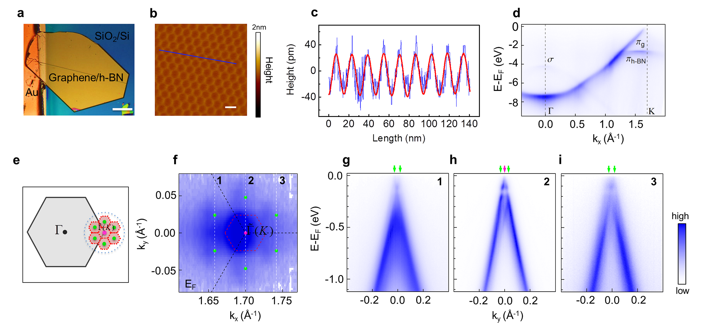
Figure 1(a,b) shows the optical and atomic force microscopic images of a typical graphene/h-BN sample that we have measured ZhangGY . Palladium (Pd) or gold (Au) electrode was deposited to ground the sample in order to avoid charging during ARPES measurements. The height profile shows that graphene exhibits significant out-of-plane height variation Å. The Moir pattern period is extracted to be nm, which is larger than 14 nm derived from the 1.8% lattice mismatch between graphene and h-BN (Fig. 1(c)). This suggests that the graphene is stretched by 0.2% by the h-BN substrate, and the reduced lattice match leads to an expanded Moir pattern. Figure 1(d) shows ARPES data measured along the -K direction. Dispersions from the and bands of both graphene and h-BN are observed, and they overlap in most regions except the band near the K point. Here, characteristic linear dispersion from the Dirac cone of graphene is observed, while the top of the band from h-BN lies at -2.2 eV, in agreement with the large band gap of h-BN. The absence of graphene band splitting confirms that the sample is dominated by monolayer graphene. An expected result of the Moir potential is the replicas of graphene Dirac cone at the same energy while translated by from the graphene K point (first generation Dirac cones, see Fig. 1(e)). The duplicated Dirac cones are obvious in both the Fermi surface map (Fig. 1(f)) and the dispersion images through the nearest SBZ centers (Fig. 1(g-i)). The average separation between the original Dirac band and its replicas is , which is consistent with the observation of expanded Moir pattern.
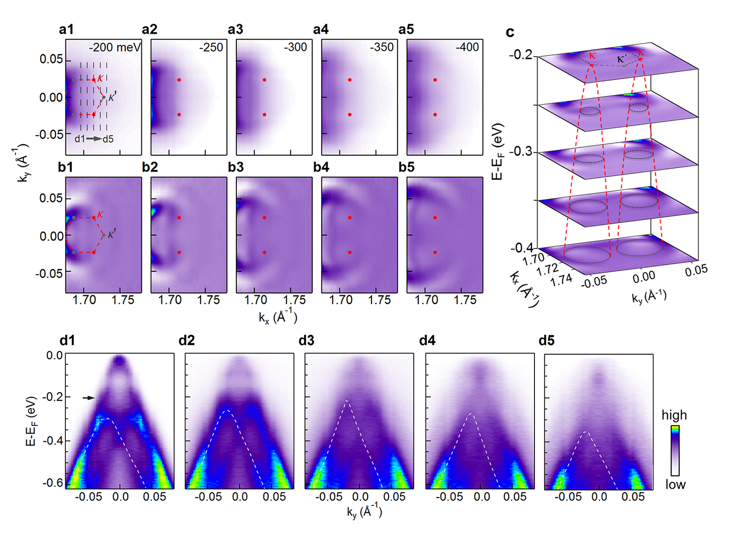
We focus on data taken near the SBZ to search for signatures of SDCs away from EF. Figure 2(a1-a5) displays intensity maps taken at constant energies between -200 to -400 meV. Corresponding curvature plots DingHRSI are used to highlight dispersive bands in ARPES data (Fig. 2(b1-b5)). At -250 meV, a small pocket is visible at the upper right and lower right corners of the SBZ (red dots, labeled as in Fig. 2(a1)), and is especially clear at -350 meV and -400 meV. The size of the pockets grows when decreasing the energy, which is consistent with conical dispersions. Dispersion images (Fig. 2(d1-d5)) taken near these corners further support the existence of conical dispersions. When approaching the second generation Dirac points (SDPs) at (cuts d1 through d3), the dispersion relations exhibit a rounded M-shape, with the top of these bands moving toward higher energies and reaching -0.21 eV at SDPs (cut d3). After passing the SDPs, the top of the valence bands move to lower energies (cuts d3 through d5), again in agreement with conical dispersion. We note that around the right corner of SBZ (labeled as ), no conical dispersion is observed, suggesting that the two superlattice valleys and are inequivalent. Therefore, both the constant energy maps and the dispersion images presented above reveal directly that SDCs exist at the SBZ corners and only at one of the two superlattice valleys JeilNcomm , which is in agreement with the Landau level degeneracy implied from previous quantum Hall effect measurements ZhangGY ; GeimNaturePhys2014 . Such direct information is critical for determining the parameters used for describing the generic band structure of SDCs FalkoMiniband ; JungPRB14 , and for further understanding other experimental results which probe the electronic structure indirectly.
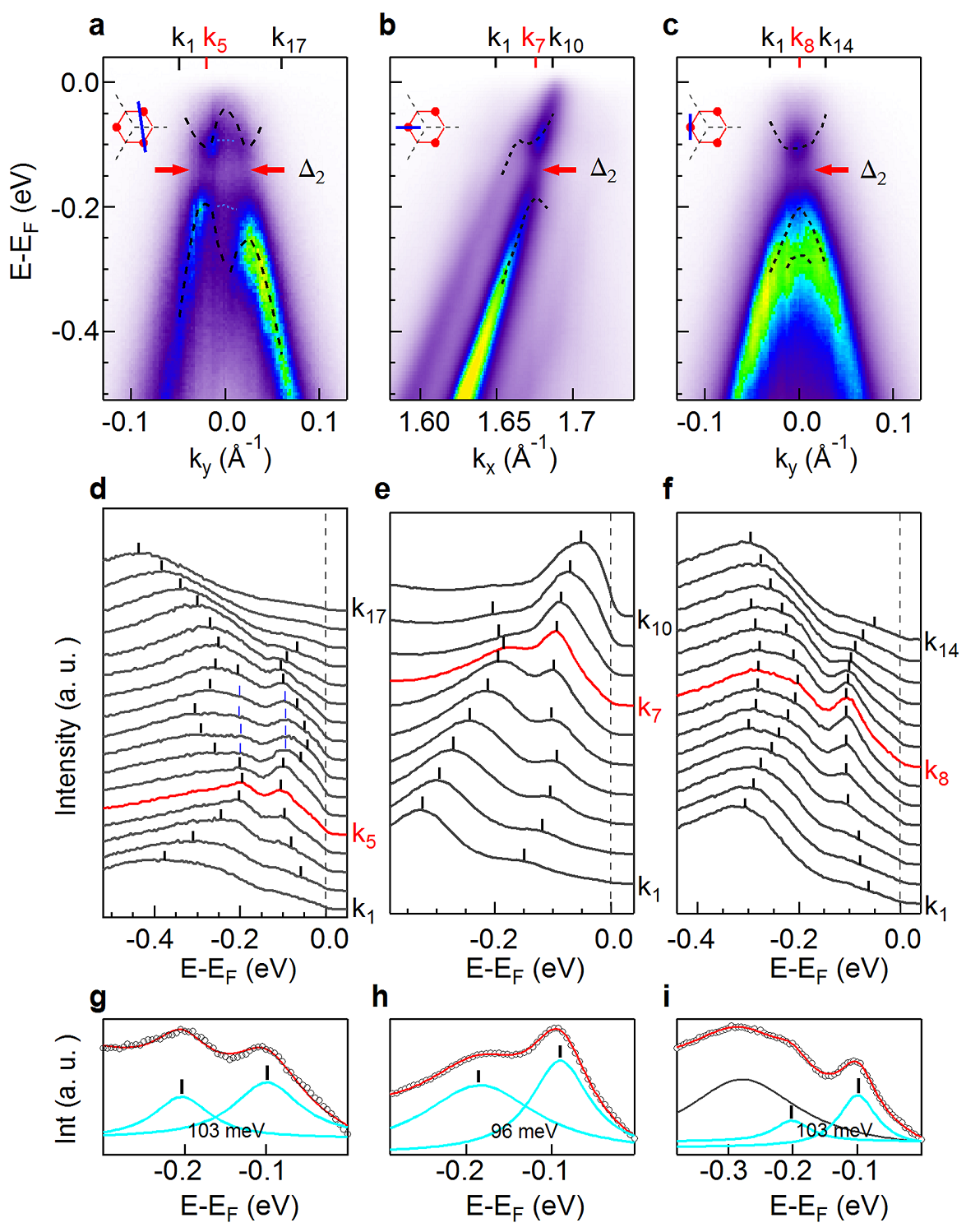
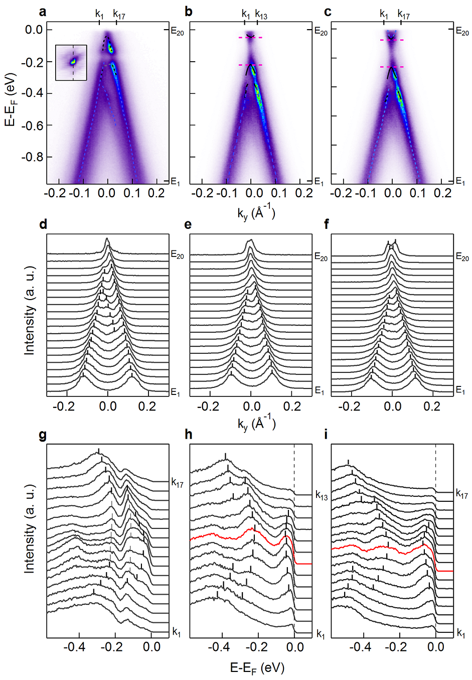
To better resolve the detailed dispersions of the SDCs, we show in Fig. 3(a) ARPES data taken near the point of the SBZ. The conduction bands and valence bands show a rounded W- and M-shape respectively with a large energy separation and a suppression of intensity between them. This indicates the gap opening at the SDCs. The corresponding energy distribution curves (EDCs) are shown in Fig. 3(d). In addition to peaks from the conduction and valence bands, there are also non-dispersive peaks (marked by blue ticks) at the band extrema, suggesting that there are significant impurity scatterings at the gap edges. From the extracted dispersions and the peak separation at the SDC (Figs. 3(g)), the gap at the SDCs is 100 meV. Direct observation of gapped SDC around the left corner of the SBZ (equivalent to the two points discussed above) in the constant energy maps is difficult, since the intensity around this momentum region is dominated by the original graphene Dirac cone. However, the intensity suppression in EDCs (Figs. 3(e,f)) from data taken along two high symmetry directions -K and -M (Figs. 3(b,c)) prove its existence with a similar gap (Figs. 3(h,i)). The observation of gapped SDCs at only one of the superlattice valleys suggest that the inversion-asymmetric perturbation potential from the h-BN substrate plays an important role in the electronic structure of graphene/h-BN.
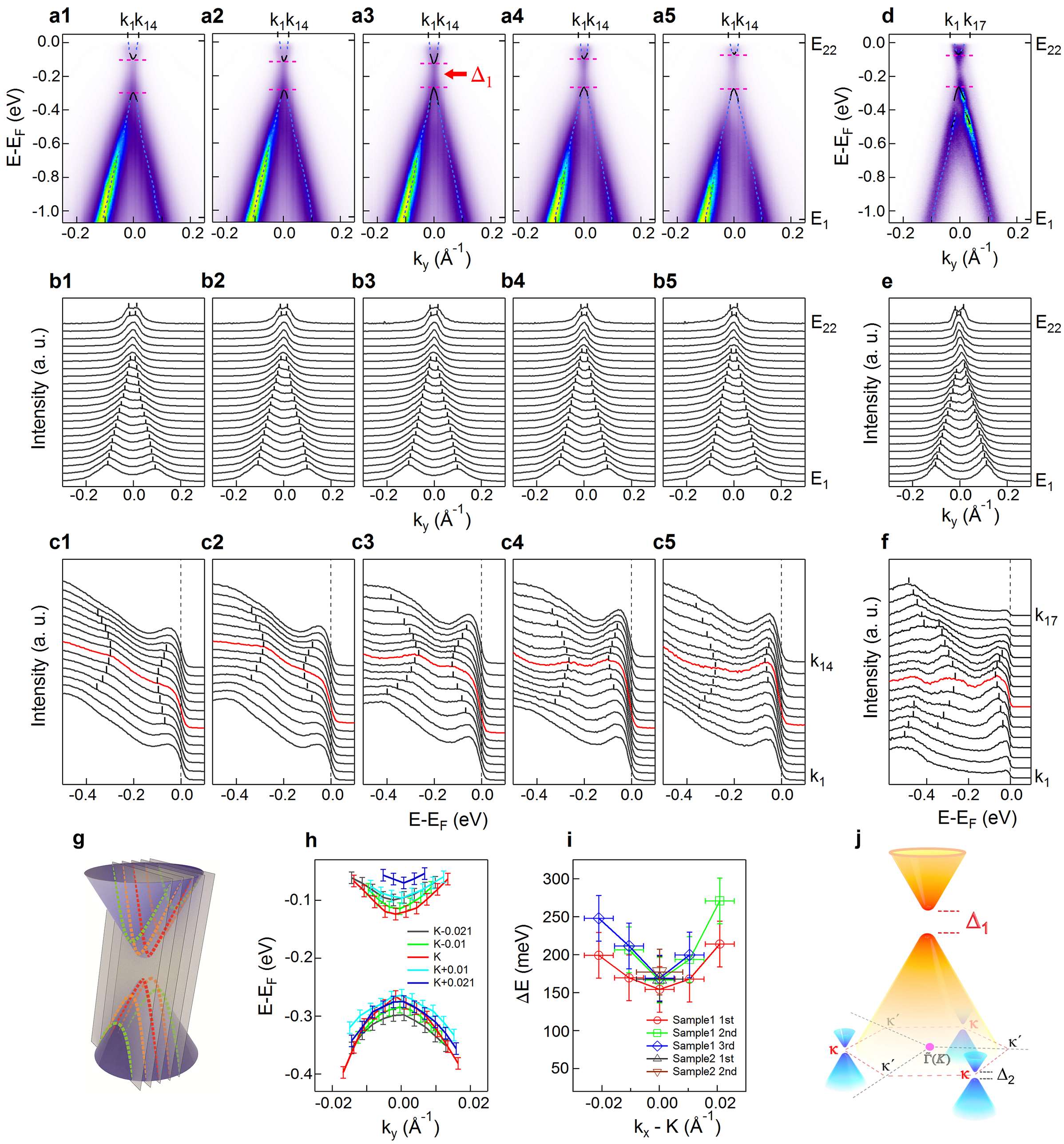
To check whether there is a gap at the original Dirac cone, we dope the graphene/h-BN sample by depositing Rubidium to shift the Dirac point below EF so that it can be measured by ARPES. By shifting the Dirac point to -0.2 eV, the conduction band becomes detectable. Figure 4(a1-a5) shows a few cuts around the K point of graphene (see schematic drawing in (g)). Because photoemitted electrons from higher binding energy have lower kinetic energy and smaller in-plane momentum component, the cutting planes are slightly tilted. The extracted dispersions from momentum distribution curves (MDCs, b1-b5) and EDCs (c1-c5) are overplotted as blue dotted and black solid curves in Fig. 4(a1-a5). Figure 4(h) focuses on the zoom-in dispersions near the Dirac point. The conduction and valence bands obviously do not touch each other when the cutting plane crosses the K point. Such behavior is an anambigous signature of an excitation gap. Figure 4(d-f) shows the data through the K point from sample 2. The dispersion is consistent with sample 1 while the intensity suppression from the gap at the SDCs is still clearly visible, likely because of the higher sample quality. Figure 4 (i) summarizes the energy separation between the conduction and valence bands. From the minimum separation at the K point, the gap is extracted to be meV. The raw data for multiple samples at all doping levels can be found in the Supplementary Information.
The extracted gap size at the original Dirac cone from ARPES measurements is much large compared to previous measurements, e.g. 1530 meV from transport measurements in transferred graphene/h-BN GBNgap ; NovoselovNphys2014 and 40 meV from magneto-optical spectroscopy on similar R-PECVD samples LiZQ , as well as theoretical predictions. Here we discuss a few reasons and the implications. First of all, since the gap is extracted from the band edges in ARPES and from the density of states in other measurements, gaps probed by other techniques can be much smaller than by ARPES since the density of states rarely drops to zero abruptly at the band edges. Impurities can also contribute to in-gap states and lead to a smaller gap size. In bilayer graphene, it has been suggested that the gap extracted from transport or STM measurements can be underestimated due to additional conductive channels by defects and charge impurities StroscioNaturePhys2011 , and this may also affect the gap size measured in graphene/h-BN. Secondly, although the maximum gap at the equilibrium layer separation for perfectly lattice matched heterostructure is predicted to be 50 meV DFTgap , the gap size increases sharply upon reducing the separation between graphene and h-BN layers DFTgap . A band gap opening at the graphene Dirac cone and SDCs can be induced by an inversion asymmetric mass term in the perturbation potential FalkoMiniband ; MoonPRB14 ; JeilNcomm , and the mass term can vary by orders of magnitude depending on the assumptions used DFTgap ; MillerPRB12 ; LevitovPRL13 . Shortening of the layer separation between graphene and h-BN by 0.2 Å around the equilibrium distance can result in almost a threefold increase of the local mass term DFTgap . Thirdly, the substantial out-of-plane height variation of 0.6 and 0.2 in-plane strain revealed by AFM measurements suggest large enough variations in the local mass term and can produce a large average gap Bokdam ; DFTgap . Therefore, the large gap size suggests that our epitaxial grown graphene/h-BN samples have much stronger short-range interlayer interaction than weak van der Waals interaction as commonly believed in ideally flat structures. Although a definitive explanation of the gap opening still requires more theoretical and experimental investigations, our work reports the intriguing electronic structure in a model van der Waals heterostructure and highlights the important role of the inversion symmetry breaking perturbation potential and interfacial atomic structure in the physics of graphene/h-BN heterostructure.
Methods
Sample preparation. Graphene samples were directly grown on h-BN substrates by the epitaxial method as specified in ref.ZhangGY . As-grown samples were characterized by tapping mode AFM (MultiMode IIId, Veeco Instruments) at room temperature in ambient atmosphere. We used freshly cleaved mica as shadow masks for metal electrode deposition. Using the micromanipulator mounted on an optical microscope, the freshly cleaved mica flakes were accurately transferred on the substrates, covering one side of the substrates with most area of target graphene/h-BN samples. The contact metal ( 40 nm Pd or Au) was deposited on the non-mica-covered area with a small part of target graphene/h-BN samples. The samples were then annealed at 200∘C, after removing the mica flakes.
ARPES measurement. ARPES measurements have been performed using ARPES instruments based at the synchrotron-radiation light source at beamline 12.0.1 of the Advanced Light Source at Lawrence Berkeley National Laboratory (LBNL). The data were recorded by Scienta R3000 at BL 12.0.1 with 50 and 60 eV photon energy. The energy and angle resolution is better than 30 meV and 0.2∘ respectively. Before measurement, the samples were annealed at 200∘C for 2-3 hours until clean surfaces were exposed. All measurements were performed between 10-20 K and under vacuum better than Torr. The Rubidium deposition was achieved by heating up SAES commercial dispenser in situ.
References
- (1) A. K. Geim I. V. Grigorieva. Van der waals heterostructures. Nature 499, 419-425 (2013).
- (2) L. A. Ponomarenko et al. Cloning of dirac fermions in graphene superlattices. Nature 497, 594-597 (2013).
- (3) C. R. Dean et al. Hofstadter’s butterfly and the fractal quantum hall effect in moire superlattices. Nature 497, 598-602 (2013).
- (4) B. Hunt et al. Massive dirac fermions and hofstadter butterfly in a van der waals heterostructure. Science 340, 1427-1430 (2013).
- (5) G. L. Yu et al. Hierarchy of hofstadter states and replica quantum hall ferromagnetism in graphene superlattices. Nature Phys. 10, 525-529 (2014).
- (6) C. R. Dean et al. Boron nitride substrates for high-quality graphene electronics. Nature Nano. 5, 722-726 (2010).
- (7) Jiamin Xue et al. Scanning tunnelling microscopy and spectroscopy of ultra-flat graphene on hexagonal boron nitride. Nature Mater. 10, 282-285 (2011).
- (8) Cheol-Hwan Park, Li Yang, Young-Woo Son, Marvin L. Cohen, Steven G. Louie. Anisotropic behaviours of massless dirac fermions in graphene under periodic potentials. Nature Phys. 4, 213-217 (2008).
- (9) Cheol-Hwan Park, Li Yang, Young-Woo Son, Marvin L. Cohen, Steven G. Louie. New generation of massless dirac fermions in graphene under external periodic potentials. Phys. Rev. Lett. 101, 126804 (2008).
- (10) J. R. Wallbank, A. A. Patel, M. Mucha-Kruczyński, A. K. Geim, V. I. Fal’ko. Generic miniband structure of graphene on a hexagonal substrate. Phys. Rev. B 87, 245408 (2013).
- (11) Carmine Ortix, Liping Yang, Jeroen van den Brink. Graphene on incommensurate substrates: trigonal warping and emerging dirac cone replicas with halved group velocity. Phys. Rev. B 86, 081405 (2013).
- (12) Pablo San-Jose, A. Gutiérrez-Rubio, Mauricio Sturla, Francisco Guinea. Spontaneous strains and gap in graphene on boron nitride. Phys. Rev. B 90, 075428 (2014).
- (13) Gianluca Giovannetti, Petr A. Khomyakov, Geert Brocks, Paul J. Kelly, Jeroen van den Brink. Substrate-induced band gap in graphene on hexagonal boron nitride: Ab initio density functional calculations. Phys. Rev. B 76, 073103 (2007).
- (14) F. Amet, J. R. Williams, K. Watanabe, T. Taniguchi, D. Goldhaber-Gordon. Insulating behavior at the neutrality point in single-layer graphene. Phys. Rev. Lett. 110, 216601 (2013).
- (15) R. V. Gorbachev et al. Detecting topological currents in graphene superlattices. Science 346, 448-451 (2014).
- (16) C. R. Woods et al. Commensurate-incommensurate transition in graphene on hexagonal boron nitride. Nature Phys. 10, 451-456 (2014).
- (17) Zhiwen Shi et al. Gate-dependent pseudospin mixing in graphene/boron nitride moire superlattices. Nature Phys. 10, 743-747 (2014).
- (18) Matthew Yankowitz et al. Emergence of superlattice dirac points in graphene on hexagonal boron nitride. Nature Phys. 8, 382-386 (2012).
- (19) Wei Yang et al. Epitaxial growth of single-domain graphene on hexagonal boron nitride. Nature Mater. 12, 792-797 (2013).
- (20) Jeil Jung, Arnaud Raoux, Zhenhua Qiao, A. H. MacDonald. Ab initio theory of moiré superlattice bands in layered two-dimensional materials. Phys. Rev. B 89, 205414 (2014).
- (21) Pilkyung Moon Mikito Koshino. Electronic properties of graphene/hexagonal-boron-nitride moiré superlattice. Phys. Rev. B 90, 155406 (2014).
- (22) M. M. van Wijk, A. Schuring, M. I. Katsnelson, A. Fasolino. Moiré patterns as a probe of interplanar interactions for graphene on h-bn. Phys. Rev. Lett. 113, 135504 (2014).
- (23) Jeil Jung, Ashley M. DaSilva, Allan H. MacDonald, Shaffique Adam. Origin of band gaps in graphene on hexagonal boron nitride. Nature Commun. 6, 6308 (2015).
- (24) Zhi-Guo Chen et al. Observation of an intrinsic bandgap and landau level renormalization in graphene/boron-nitride heterostructures. Nature Commun. 5, 4461 (2014).
- (25) Menno Bokdam, Taher Amlaki, Geert Brocks, Paul J. Kelly. Band gaps in incommensurable graphene on hexagonal boron nitride. Phys. Rev. B 89, 201404 (2014).
- (26) P. Zhang et al. A precise method for visualizing dispersive features in image plots. Rev. Sci. Instrum. 82, 043712 (2011).
- (27) G.M. Rutter, S. Jung, N.N. Klimov, D.B. Newell, N.B. Zhitenev J.A. Stroscio. Microscopic polarization in bilayer graphene. Nature Phys. 7, 649 (2011).
- (28) M. Kindermann, Bruno Uchoa, D.L. Miller. Zero-energy modes and gate-tunable gap in graphene on hexagonal boron nitride. Phys. Rev. B 86, 115415 (2012).
- (29) Justin C. W. Song, Andrey V. Shytov, Leonid S. Levitov. Electron interactions and gap opening in graphene superlattices. Phys. Rev. Lett. 111, 266801 (2013).
Acknowledgements We thank V.I. Fal’ko for the useful discussions. This work is supported by the National Natural Science Foundation of China (Grant No. 11274191, 11334006, and 11427903), Ministry of Science and Technology of China (Grant No. 2015CB921001, 2016YFA0301004) and Tsinghua University Initiative Scientific Research Program (2012Z02285). E.Y.W. thanks support from the Advanced Light Source doctoral fellowship program. The Advanced Light Source is supported by the Director, Office of Science, Office of Basic Energy Sciences, of the U.S. Department of Energy under Contract No. DE-AC02-05CH11231.
Author Contributions S.Z. designed the research project. E.W., S.D., W.Y., M.Y., G.W., K.D., A.V.F. and S.Z. performed the ARPES measurements and analyzed the ARPES data. X.L., S.W., G.C., G.Z and Y. Z. prepared the graphene samples. J.J. discussed the data. E.W. and S.Z. wrote the manuscript, and all authors commented on the manuscript.
Competing financial interests The authors declare no competing financial interests.
Supplementary Information
I Raw data at different doping levels of different samples
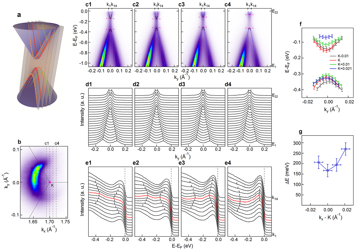
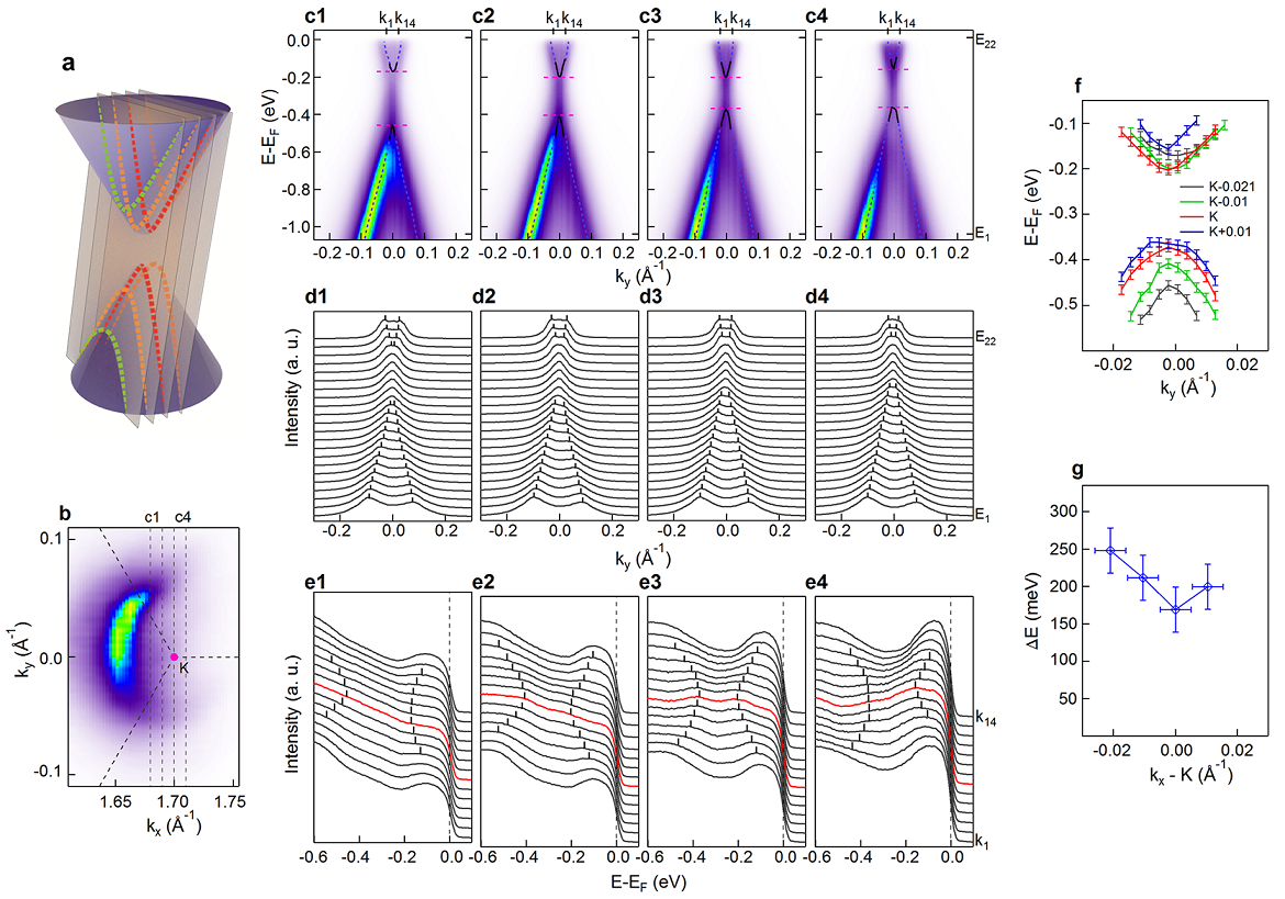
For determining the gap size at the original Dirac point, in order to avoid the artifact due to derivation from K point, we first took maps around K point by step to determine the accurate position of Dirac point. The errorbar of the Dirac point position is within in this case, which converts to 0.006 and 0.0066 for 50 and 60 eV photo energy respectively. For sample 1, we took several cuts around the Dirac point after each doping (Fig. 4, Fig. S5, S6). The panels (c1-c4) in Fig. S5 and Fig. S6 show the band dispersions near the Dirac point for sample1 after 2nd and 3rd doping. The extracted dispersions from peaks in the momentum distribution curves (MDCs, panels (d1-d4)) where the band dispersions are linear and the energy distribution curves (EDCs, panels (e1-e4)) near the Dirac point are overplotted as blue dotted and black solid lines in panels (c1-c4), and the zoom-in dispersions near the Dirac point are shown in panel (f). The bottom of conduction band and the top of valence band do not touch each other when the cutting plane crosses the K point, signalling the gap opening at the original Dirac point, consistent with the conclusions in main text. The evolution of the minimum separation between the valence and conduction bands measured at each cut across the original Dirac cone is shown in panel(g). For sample 2, we deposited Rubidium on sample surface in situ after moving sample to the angle corresponding to the K point. The suppression of intensity at the original Dirac point is also visible after shifting Dirac point below Fermi energy which signals gap opening (Fig. S7). The evolution of the minimum separation between the valence and conduction bands measured at each cut around the original Dirac cone from sample 1 and sample 2 at different doping levels is summarized in Fig. 4(i).