Lead-Free Halide Double Perovskites via Heterovalent Substitution of Noble Metals.
Abstract
Lead-based halide perovskites are emerging as the most promising class of materials for next generation
optoelectronics. However, despite the enormous success of lead-halide perovskite solar
cells, the issues of stability and toxicity are yet to be resolved. Here
we report on the computational design and the experimental synthesis of a new family of Pb-free
inorganic halide double-perovskites based on bismuth or antimony and noble metals. Using
first-principles calculations we show that this hitherto unknown family of perovskites
exhibits very promising optoelectronic properties, such as tunable band gaps in the visible range and
low carrier effective masses. Furthermore, we successfully synthesize the
double perovskite Cs2BiAgCl6, we perform structural refinement using
single-crystal X-ray diffraction, and we characterize its optical properties via optical absorption
and photoluminescence measurements. This new perovskite belongs to the space group,
and consists of BiCl6 and AgCl6 octahedra alternating in a rock-salt face-centered cubic structure.
From UV-Vis and PL measurements we obtain an indirect gap of 2.2 eV. The new compound
is very stable under ambient conditions.
Table of Contents Image
![[Uncaptioned image]](/html/1603.01585/assets/toc.png)
Keywords: Noble-metal halide double perovskites, Lead-free perovskites, Computational design, materials synthesis, structure refinement, UV-Vis spectra, Photoluminescence spectra
These authors contributed equally to this work Department of Materials, University of Oxford]Department of Materials, University of Oxford, Parks Road OX1 3PH, Oxford, UK \altaffiliationThese authors contributed equally to this work Department of Materials, University of Oxford]Department of Materials, University of Oxford, Parks Road OX1 3PH, Oxford, UK Department of Physics, University of Oxford]Department of Physics, University of Oxford, Clarendon Laboratory, Parks Road, Oxford OX1 3PU, UK Department of Physics, University of Oxford]Department of Physics, University of Oxford, Clarendon Laboratory, Parks Road, Oxford OX1 3PU, UK Department of Physics, University of Oxford]Department of Physics, University of Oxford, Clarendon Laboratory, Parks Road, Oxford OX1 3PU, UK Department of Physics, University of Oxford]Department of Physics, University of Oxford, Clarendon Laboratory, Parks Road, Oxford OX1 3PU, UK \phone(+44) 1865 612790 Department of Materials, University of Oxford]Department of Materials, University of Oxford, Parks Road OX1 3PH, Oxford, UK \phone(+44) 01865 272380
Perovskites are among the most fascinating crystals, and play important roles in a variety of applications, including ferroelectricity, piezzoelectricity, high-Tc superconductivity, ferromagnetism, giant magnetoresistance, photocatalysis and photovoltaics 1, 2, 3, 4, 5, 6, 7, 8. The majority of perovskites are oxides and are very stable under ambient temperature and pressure conditions 4, 9. However, this stability is usually accompanied by very large band gaps, therefore most oxide perovskites are not suitable candidates for optoelectronic applications. The most noteworthy exceptions are the ferroelectric perovskite oxides related to LiNbO3, BaTiO3, Pb(Zr, Ti)O3 and BiFeO3, which are being actively investigated for photovoltaic applications, reaching power conversion efficiencies of up to 8%9. The past five years witnessed a revolution in optoelectronic research with the discovery of the organic-inorganic lead-halide perovskite family. These solution-processable perovskites are fast becoming the most promising materials for the next generation of solar cells, achieving efficiencies above 20% 10, 11, 12, 13. Despite this breakthrough, hybrid lead-halide perovskites are known to degrade due to moisture and heat 14, upon prolonged exposure to light, 15 and are prone to ion or halide vacancy migration, leading to unstable operation of photovoltaic devices 16, 17. At the same time the presence of lead raises concerns about the potential environmental impact of these materials 18, 19. Given these limitations, identifying a stable, non-toxic halide perovskite optoelectronic material is one of the key challenges to be addressed in the area of perovskite optoelectronics.
The starting point of our search for a lead-free halide-perovskite is the prototypical inorganic compound of the family CsPbI3. CsPbI3 is an ABX3 perovskite where the heavy metal cations Pb2+ and the halide anions I- occupy the B and X sites, respectively, while Cs+ occupies the A site. The most obvious route to replacing Pb in this compound is via substitution of other group-14 elements such as Sn and Ge. However both elements tend to undergo oxidation, for example from Sn2+ to Sn4+, leading to a rapid degradation of the corresponding halide perovskites 20, 21, 22, 23. More generally, it should also be possible to substitute lead by other divalent cations outside of group-14 elements. However, our previous high-throughput computational screening of potential candidates showed that the homovalent substitution of lead in halide perovskites impacts negatively the optoelectronic properties by increasing band gaps and effective masses 24.
Another possible avenue is to consider heterovalent substitution, that is the formation of a double perovskite structure with a basic formula unit A2BB′X6 4. This type of compounds are abundant in the case of oxides and are well known for their ferroelectric, ferromagnetic and multiferroic properties 4. Additionally, double perovskites have been explored in order to tune the band gap of oxide perovskites 25, 26. On the other hand, halide double perovskites remain a much less explored class of materials. To date, the best known halide double perovskites are based on alkali and rare-earth metals, and are investigated for applications as scintillators in radiation detectors 27.
In order to replace the divalent Pb cations and maintain the total charge neutrality, the B′ and B′′ sites have to be occupied by one monovalent and one trivalent cation. We search for our B′3+ metallic cations among the pnictogens, and consider Bi and Sb as the most suitable choices. Arsenic is less desirable owing to its toxicity. For the monovalent cations we choose the noble metals Cu, Ag and Au. From elementary considerations Cu, Ag, and Au appear very promising for optoelectronic applications. In fact, in their metallic form, the noble metals are the best known electrical conductors, owing to their filled shell and the free-electron-like behaviour of the shell. In addition, in an octahedral environment, the ionic radii of Cu+ (0.91 Å), Ag+ (1.29 Å) and Au+ (1.51 Å) are similar to those of Pb2+ (1.19 Å), Sb3+ (0.76 Å) and Bi3+ (1.03 Å) 28. Following this simple reasoning we investigate hypothetical halide double perovskites with the pairs B′/B′′ where B′ = Sb, Bi, and B′′ = Cu, Ag, Au.
We investigate the electronic properties of these hypothetical compounds from first principles using density functional theory (DFT) in the local density approximation (LDA). We construct ‘rock-salt’ double perovskites, whereby B′ and B′′ alternate in every direction (shown in Figure 1a). The rock-salt ordering is known to be the ground state for most oxide double perovskites 4, therefore it can be expected to hold also in the present case. For each model structure we perform full structural optimization using DFT-LDA and calculate the electronic band gaps using the hybrid PBE0 functional as described in the Supporting Information.
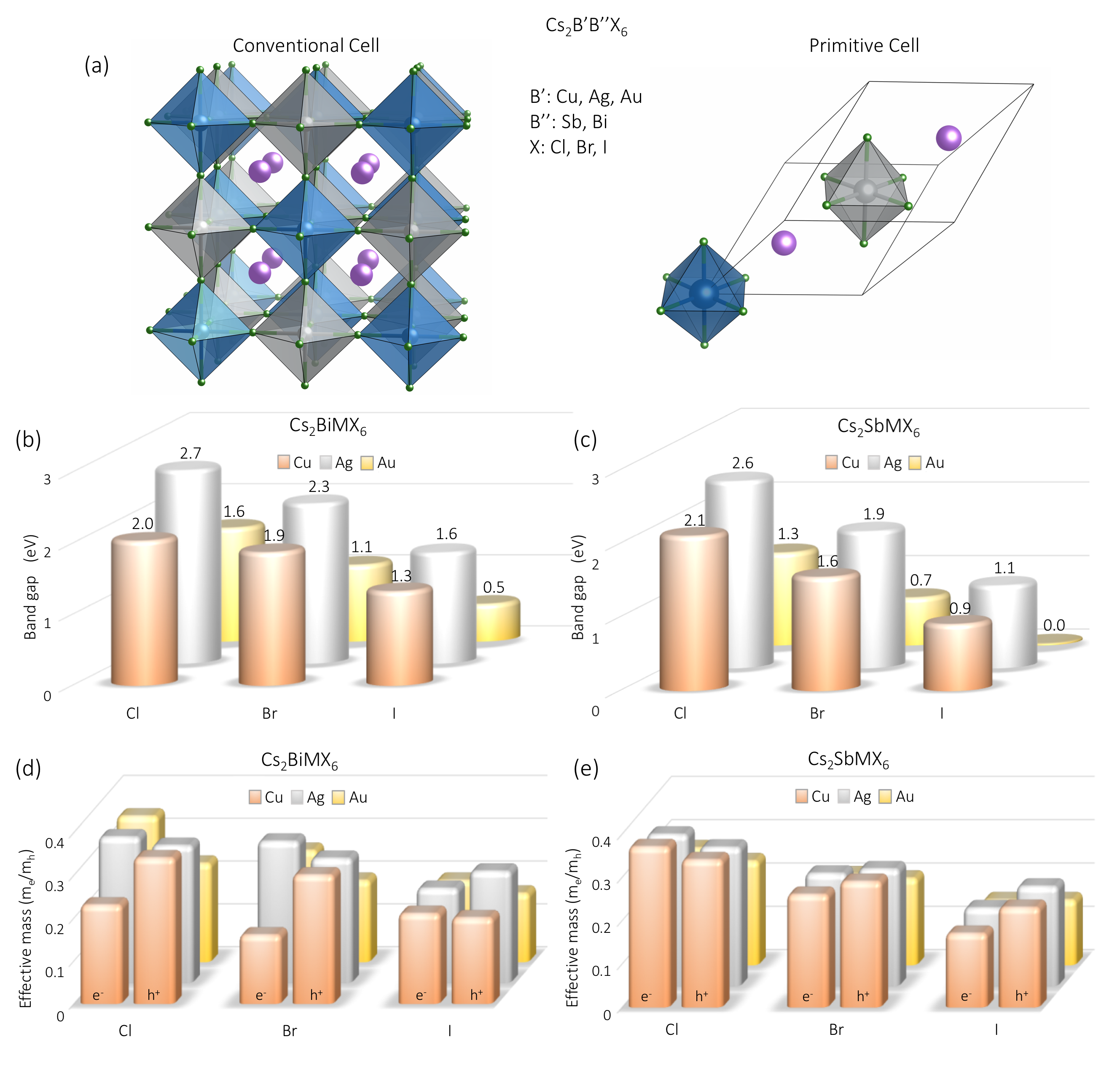
a Polyhedral model of the conventional (left) and reduced (right) unit cell of the hypothetical halide double perovskites. The pnictogen (B′) and noble metal (B′′) cations alternate along the three crystallographic axes, forming the rock-salt ordering. b Electronic band gaps calculated for all compounds in the halide double perovskite family using the PBE0 hybrid functionals. All calculated band gaps are indirect with the top of the valence band at the X point (0,0,) of the Brillouin zone, where is the lattice parameter of the FCC unit cell. The bottom of the conduction band is at the L point (, , ) of the Brillouin zone in all cases, except Cs2BiAgCl6, Cs2BiCuCl6 and Cs2BiCuBr6 where the bottom of the conduction band is found at the (0,0,0) point. c Transport effective masses calculated from DFT/LDA for each compound (see Supporting Information). The effective masses are calculated at the VBM (holes) and CBM (electrons) in each case.
In Figure 1b-c we show a comparative view of the band gaps calculated for the entire Cs2B′B′′X6 family. We find that all band gaps are below 2.7 eV, spanning the visible and near infrared optical spectrum. The band gaps are indirect and increase as we move up the halogen or the pnictogen column in the periodic table, but do not follow a monotonic trend with respect to the size of the noble metal cation. This behaviour can be explained by the character of the electronic states at the band edges. Indeed, a shown in Figure S1 of the Supporting Information, the conduction band bottom and valence band top in each case are predominantly of pnictogen- and halogen- character, respectively. As we move up in the periodic table the energy of the halogen- states decreases, thus lowering the energy of the valence band top. Similarly, the energy of the pnictogen- states decreases when moving up in the periodic table, thus lowering the energy of the conduction band bottom. The electron and hole effective masses calculated at the band edges exhibit an anisotropic behaviour in most cases (see Table S1). Throughout the entire family of compounds the electron masses are more isotropic than the hole masses. For clarity, in Figure 1 we report the transport effective masses 29, as defined in the Supporting Information. We note that all compounds exhibit small carrier effective masses between 0.1 and 0.4 , very close to those calculated for CH3NH3PbI3 within the same level of theory 30.
The electronic band structures of these halide double perovskites (shown in Figure S2 and S3) exhibit several features of particular interest. In all cases, the valence band maximum (VBM) is at the (0,0,) point in the Brillouin zone. The conduction band minimum (CBM) is at (0,0,0) for Cs2BiAgCl6, Cs2BiCuCl6 and Cs2BiCuBr6, while for the other compounds the CBM is at the (, , ) point. The FCC cubic crystals of the former three compounds are indirect band gap semiconductors, however a small disturbance of the conventional unit cell symmetry could render the direct optical transition allowed. This is shown in Figure S4, where the band structure of Cs2BiAgCl6 is calculated in the conventional unit cell (which corresponds to two primitive cells). Here, as a result of Brillouin zone folding in the conventional FCC unit cell, the band gap of Cs2BiAgCl6 becomes direct at the point. In practice, this effect could be realized by incorporating an organic cation, like methylammonium (CH3NH) or formamidinium (CHN2H) into the cuboctahedral cavity. We illustrate this possibility by calculating the band structure of the hypothetical orthorhombic CH3NH3BiAgCl6 (constructed as described in the Supporting Information); as expected we obtain a direct band gap, as shown in Figure S5.
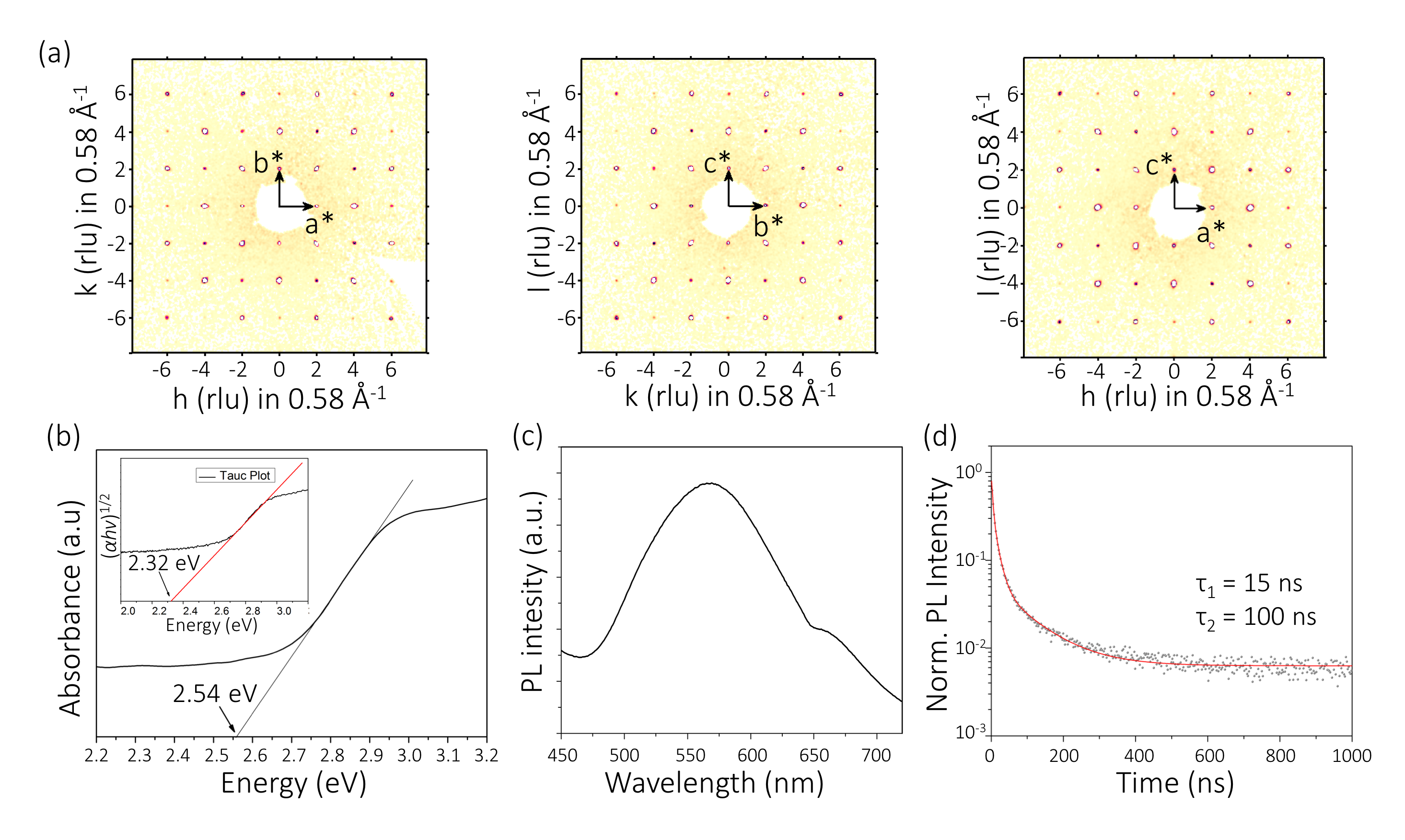
a X-ray diffraction pattern for a Cs2BiAgCl6 single crystal at 293 K. shown for three different planes, i.e. , and . All wave vectors are labeled in reciprocal lattice units (rlu) and a∗, b∗ and c∗ denote reciprocal lattice vectors of the cubic cell of the structure. b UV-Vis optical absorption spectrum of Cs2BiAgCl6. The inset shows the Tauc plot, corresponding to an indirect allowed transition [assuming the expression: , where is the absorption coefficient, is the energy of the incoming photon is the optical band gap and is a constant]. The straight lines are fitted to the linear regions of the absorption spectrum and Tauc plot, and the intercepts at 2.32 eV and 2.54 eV marked on the plot are calculated from the fit. c Steady-state photoluminescence (PL) spectrum of Cs2BiAgCl6, deposited on glass. d Time resolved photoluminescence decay of Cs2BiAgCl6, deposited on glass. The data is fitted using a biexponential decay function. The decay lifetimes of 15 ns (fast) and 100 ns (slow) is estimated from the fit.
Having established that the family of A2BB′X3 halide double perovskites, based on B = Sb, Bi and B′ = Cu, Ag, Au exhibits promising optoelectronic properties, we move to the synthesis and optical characterization of a representative member of this group of compounds. We adapt the synthesis process of Cs2BiNaCl6, reported in Ref. 31, to allow for the incorporation of a noble metal. Of the three noble metals under consideration, Ag has an ionic radius which is closest to that of Na (1.02 Å vs 1.15 Å). For this reason we proceed to synthesize Cs2BiAgCl6 by conventional solid-state reaction as described in detail in the Supporting Information. In Figure 2a we show the X-ray Diffraction Pattern for a single crystal (30m diameter). We observe sharp reflections for the crystallographic , and planes. These reflections show characteristics of mm symmetry that reveal systematic absences for (; , , ) corresponding to the face-centered space groups , and . The latter was selected for structure refinement after confirmation that Cs2BiAgCl6 crystallizes in an FCC lattice. We find that there is no significant distortion of octahedral symmetry about the Bi3+. The atomic positions from the structural refinement are listed in Table S2 of the Supplementary Information. The X-ray diffraction patterns uniquely identify the (no. 225) space group at room temperature, and the quantitative structural analysis gives a very good description of the data. In addition, our crystal structure refinement is consistent with the rock-salt configuration assumed by our atomistic model. The experimental and computationally predicted conventional lattice parameters are in very good agreement, 10.78 Å and 10.50 Å, respectively. From the optical absorption spectrum and Tauc plot (see Figure 2b) we can estimate an indirect optical band gap in the range of 2.3-2.5 eV. The indirect character of the band gap is consistent with the broad photoluminescence peak observed between 480 and 650 nm (1.9-2.6 eV) with the maximum at 575 nm (2.2 eV), red-shifted with respect to the optical absorption onset. In addition, the time-resolved photoluminescence decay shown in Figure 2c was fitted with a double exponential giving a fast component lifetime of 15 ns and a slow component lifetime of 100 ns.
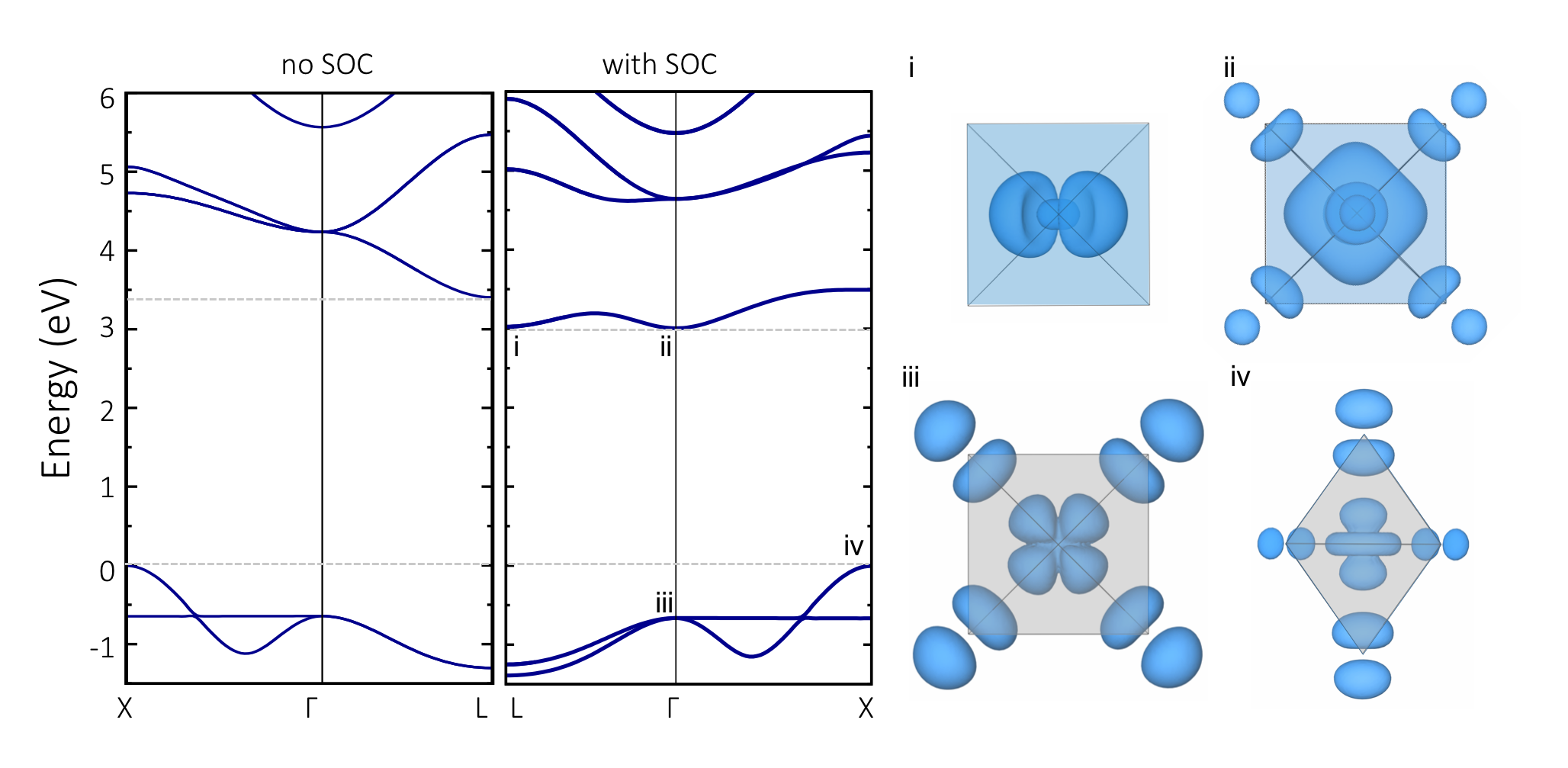
The Band structure of Cs2BiAgCl6 calculated along the high symmetry path L() - (0,0,0) - X (0,0,2/a) without (left) and with (right) spin-orbit coupling. The black points on the fully relativistic band structure marked ‘i-iv’ mark the conduction band bottom at L and and the valence band top at and X, respectively. For each of the states we show the electronic wavefunctions. The conduction band bottom is primarily of Bi- and Cl- character, while the valence band top consists of Ag- and Cl- character. The shape of all four wavefunctions is consistent with metal-halide -bonds.
In Figure 3 we show the electronic band structure of Cs2BiAgCl6 calculated for the as determined experimental crystal structure, with and without relativistic spin-orbit coupling effects. The features of the valence band edge are almost unchanged when the relativistic effects are included. This is consistent with the predominant Cl- and Ag- character of this band. By contrast, due to the large spin-orbit coupling, the conduction band edge splits in two bands, separated by more than 1.5 eV at the point. This effect is not surprising, given that the character of the conduction band bottom is of primarily Bi- character. For comparison, in the case of Cs2SbAgCl6 (see Figure S7) the spin-orbit splitting of the conduction band at the point is of only 0.5 eV. The fundamental band gap is reduced by 0.4 eV upon inclusion of relativistic effects, and the shape of the conduction band is drastically different. Therefore, the inclusion of spin-orbit coupling is crucial for the correct description of the conduction band edge, bearing resemblance to the case of CH3NH3PbI3 32, 33. In the fully relativistic case we calculated an indirect band gap of 3.0 eV and lowest direct transition of 3.5 eV, in very close agreement with the results obtained for the model Cs2BiAgCl6 structure, discussed in Figure 1 [2.7 eV (indirect) and 3.3 eV (direct)]. The small difference in band gap of 0.2-0.3 eV is due to the small difference in volume between the experimental and predicted crystal structure. The calculated electronic band gaps are overestimated with respect to the measured optical band gap by approximately 0.5 eV. This quantitative discrepancy does not affect the qualitative physical trends of the band gaps discussed throughout this work, and can be associated to the approximations employed in our PBE0 calculations. A better agreement with experiment can be reached by fine-tuning the fraction of exact exchange, or by performing calculations 34, 35. The latter will be reported in a future work.
In summary, through a combined theoretical and experimental study, we have designed a new family of halide double-perovskite semiconductors based on pnictogens and noble metals. These compounds have promising electronic properties, such as low carrier effective masses and band gaps covering the visible and near-infrared region of the optical spectrum. All compounds are indirect gap semiconductors and exhibit strong spin-orbit coupling. We successfully synthesized Cs2BiAgCl6, and obtained a face-centered cubic double perovskite, exhibiting optical properties consistent with an indirect gap semiconductor, in agreement with our computational predictions. The present work is the first detailed description of the structure and optoelectronic properties of the pnictogen-noble metal halide double perovskite family, and calls for many future experimental and theoretical studies in order to assess the full potential of these new materials. We expect that a complete mapping of the genome of halide double perovskites based on pnictogens and noble metals may unlock a world of new exciting optoelectronic materials for solar cells, photodetectors, light-emitting devices, and transistors.
The research leading to these results has received funding from the the Graphene Flagship (EU FP7 grant no. 604391), the Leverhulme Trust (Grant RL-2012-001), the UK Engineering and Physical Sciences Research Council (Grant No. EP/J009857/1 and EP/M020517/1), and the European Union Seventh Framework Programme (FP7/2007-2013) under grant agreements n∘239578 (ALIGN) and n∘604032 (MESO). The authors acknowledge the use of the University of Oxford Advanced Research Computing (ARC) facility (http://dx.doi.org/ 10.5281/zenodo.22558) and the ARCHER UK National Supercomputing Service under the ‘AMSEC’ Leadership project. G.V., M.R.F. and F.G. would like to thank Marios Zacharias for useful discussions. Figures involving atomic structures were rendered using VESTA 36.
Note added
During the preparation of this manuscript we became aware of the publication of two related papers: Ref. 37 (published February 7th, 2016) and Ref. 38 (published February 10th, 2016). The key difference between the present work and that of Ref. 37, 38 is that we perform a computational screening of the entire family of pnictogen-noble metal double halide perovskites and perform experiments that confirm our predictions.
References
- Suntivich et al. 2011 Suntivich, J.; Gasteiger, H. A.; Yabuuchi, N.; Nakanashi, H.; Goodenough, J. B.; Shao-Horn, Y. Design principles for oxygen-reduction activity on perovskite oxide catalysts for fuel cells and metal–air batteries. Nature Chemistry 2011, 3, 546–550
- Stranks and Snaith 2015 Stranks, S.; Snaith, H. J. Metal-Halide Perovskites for Photovoltaic and Light-Emitting Devices. Nature Nanotechology 2015, 10, 391
- Grätzel 2014 Grätzel, M. The Light and Shade of Perovskite Solar Cells. Nature Materials 2014, 13, 838
- Vasala and Karppinen 2015 Vasala, S.; Karppinen, M. A2B′B″O6 perovskites: A review. Prog. Solid State Chem. 2015, 4, 1–36
- Grinberg et al. 2013 Grinberg, L.; West, D. V.; Torres, M.; Gou, G.; Stein, D. M.; Wu, L.; Chen, G.; Gallo, E. M.; Akbashev, A. R.; Davies, P. K.; Spanier, J. E.; Rappe, A. M. Perovskite oxides for visible-light-absorbing ferroelectric and photovoltaic materials. Nature 2013, 503, 509–512
- Ramesh and Spaldin 2007 Ramesh, R.; Spaldin, N. A. Multiferroics: progress and prospects in thin films. Nature Mater. 2007, 6, 21–29
- Rinjders and Blank 2005 Rinjders, G.; Blank, D. H. A. Materials science: Build your own superlattice. Nature 2005, 433, 369–370
- Ahn et al. 2004 Ahn, C. H.; Rabe, K. M.; Triscone, J.-M. Ferroelectricity at the Nanoscale: Local Polarization in Oxide Thin Films and Heterostructures. Science 2004, 303, 488–491
- Fan et al. 2015 Fan, Z.; Sun, K.; Wang, J. Perovskites for photovoltaics: a combined review of organic–inorganic halide perovskites and ferroelectric oxide perovskites. J. Mater. Chem. A 2015, 3, 18809
- Green et al. 2014 Green, M.; Ho-Baillie, A.; Snaith, H. J. The Emergence of Perovskite Solar Cells. Nature Photonics 2014, 8, 506
- Lee et al. 2012 Lee, M. M.; Teuscher, J.; Miyasaka, T.; Myrakami, T. N.; Snaith, H. J. Efficient Hybrid Solar Cells Based on Meso-Superstructured Organometal Halide Perovskites. Science 2012, 338, 643
- Kim et al. 2012 Kim, H.-S.; Lee, C. R.; Im, J.-H.; Lee, K.-B.; Moehl, T.; Marchioro, A.; Moon, S.-J.; Humphry-Baker, R.; Yum, J.-H.; Moser, J. E.; M., G.; N.-G., P. Lead Iodide Perovskite Sensitized All-Solid-State Submicron Thin Film Mesoscopic Solar Cell with Efficiency Exceeding 9%. Sci. Rep. 2012, 2, 591
- 13 Best Research-Cell Efficiencies. \urlhttp://www.nrel.gov/ncpv/images/efficiency_chart.jpg
- Manser et al. 2016 Manser, J. S.; Saidaminov, M. I.; Christians, J. A.; Bakr, O. M.; Kamat, P. V. Making and breaking of lead-halide perovskites. Acc. Chem. Res. 2016,
- Hoke et al. 2015 Hoke, E. T.; Slotcavage, D. J.; Dohner, E. R.; Bowring, A. R.; Karunadasa, H. I.; McGehee, M. D. Reversible photo-induced trap formation in mixed-halide hybrid perovskites for photovoltaics. Chem. Sci. 2015, 6, 613–617
- Eames et al. 2015 Eames, C.; Frost, J. M.; Barnes, P. R. F.; O’Regan, A., B. C.and Walsh; Saiful Islam, M. Ionic transport in hybrid lead iodide perovskite solar cells. Nature Commun. 2015, 6, 7497
- Meloni et al. 2016 Meloni, S.; Moehl, T.; Tress, W.; Grankvicius, M.; Saliba, M.; Hui, Y.; Gao, P.; Nazeeruddin, M. K.; Zakeeruddin, S. M.; Rothlisberger, U.; Grätzel, M. Ionic polarization induced current-voltage hysteresis in CH3NH3PbX3 perovskite solar cells. Nature Commun. 2016, 7, 10334
- Espinosa et al. 2015 Espinosa, N.; Serrano-Luján, L.; Urbina, A.; Krebs, F. C. Solution and Vapour Deposited Lead Perovskite Solar Cells: Ecotoxicity from a Life Cycle Assessment Perspective. Solar Energy Materials and Solar Cells 2015, 137, 303
- Babagayigit et al. 2016 Babagayigit, A.; Thanh, D. D.; Ethirajan, A.; Manca, J.; Muller, M.; Boyen, H.-G.; Conings, B. Assessing the toxicity of Pb- and Sn-based perovskite solar cells in model organism Danio rerio. Sci. Rep. 2016, 6, 18721
- Stoumpos et al. 2013 Stoumpos, C. C.; Malliakas, C. D.; Kanatzidis, M. G. Semiconducting Tin and Lead Iodide Perovskites with Organic Cations: Phase Transitions, High Mobilities, and Near-Infrared Photoluminescent Properties. Inorg. Chem. 2013, 52, 9019
- Baikie et al. 2013 Baikie, T.; Fang, Y.; Kadro, J. M.; Schreyer, M.; Wei, F.; Mhaisalkar, S. G.; Grätzel, M.; White, T. J. Synthesis and Crystal Chemistry of the Hybrid Perovskite (CH3NH3PbI3) for Solid-State Sensitized Solar Applications. J. Chem. Mater. A 2013, 1, 5628
- Hao et al. 2014 Hao, F.; Stoumpos, C. C.; Cao, D. H.; Chang, R. P. H.; Kanatzidis, M. G. Lead-free Solid-State Organic-Inorganic Halide Perovskite Solar Cells. Nature Photonics 2014, 8, 489
- Noel et al. 2014 Noel, N.; Stranks, S. D.; Abate, A.; Wehrenfennig, C.; Guarnera, S.; Haghighirad, A.-A.; Sadhanala, A.; Eperon, G. E.; Pathak, S. K.; Johnston, A., M. B. andPetrozza; Herz, L. M.; Snaith, H. J. Lead-Free Organic-Inorganic Tin Halide Perovskite for Photovoltaic Applications. Energ. Environ. Sci 2014, 7, 3061
- Filip and Giustino 2016 Filip, M. R.; Giustino, F. Computational Screening of Homovalent Lead Substitution in Organic−Inorganic Halide Perovskites. J. Phys. Chem. C 2016, 120, 166–173
- Nechache et al. 2015 Nechache, R. N.; Harnagea, C.; Li, S.; Cardenas, L.; Huang, W.; Chakrabartty, J.; Rosei, F. Bandgap tuning of multiferroic oxide solar cells. Nature Photon. 2015, 9, 61–67
- Berger and Neaton 2012 Berger, R. F.; Neaton, J. B. Computational design of low-band-gap double perovskites. Phys. Rev. B 2012, 86, 165211
- van Loef et al. 2002 van Loef, E. V. D.; Dorenbos, P.; van Eijk, C. W. E.; Krämer, K. W.; Güdel, H. U. Scintillation and spectroscopy of the pure and Ce3+-doped elpasolites: Cs2LiYX6 (X = Cl, Br). J. Phys.: Condens. Matter. 2002, 14, 8481–8496
- Shannon 1976 Shannon, R. D. Revised effective ionic radii and systematic studies of interatomic distances in halides and chalcogenides. Acta. Cryst. A 1976, 32, 751–767
- He and Galli 2014 He, Y.; Galli, G. Perovskites for Solar Thermoelectric Applications: a First Principle Study of CH3NH3AI3 (A = Pb and Sn). Chem. Mater. 2014, 26, 5394
- Filip et al. 2015 Filip, M. R.; Verdi, C.; Giustino, F. GW Band Structures and Carrier Effective Masses of CH3NH3PbI3 and Hypothetical Perovskites of the Type APbI3: A = NH4, PH4, AsH4 and SbH4. J. Phys. Chem. C 2015, 119, 25209–25219
- Morrs and Robinson 1972 Morrs, L. R.; Robinson, W. R. Crystal structure of Cs2BiNaCl6. Acta Cryst. B 1972, 28, 653–654
- Even et al. 2013 Even, J.; Pedesseau, L.; Jancu, J.-M.; Katan, C. Importance of Spin-Orbit Coupling in Hybrid Organic/Inorganic Perovskites for Photovoltaic Applications. J. Phys. Chem. Lett. 2013, 4, 2999
- Filip and Giustino 2014 Filip, M. R.; Giustino, F. GW Quasiparticle Band Gap of the Hybrid Organic-Inorganic Perovskite CH3NH3PbI3: Effect of Spin-Orbit Interaction, Semicore Electrons, and Self-Consistency. Phys. Rev. B 2014, 90, 245145
- Hedin 1965 Hedin, L. New Method for Calculating the One-Particle Green’s Function with Application to the Electron-Gas Problem. Phys. Rev. 1965, 139, A796
- Hybertsen and Louie 1986 Hybertsen, M. S.; Louie, S. G. Electron Correlation in Semiconductors and Insulators: Band Gaps and Quasiparticle Energies. Phys. Rev. B 1986, 34, 5390
- Momma and Izumi 2008 Momma, K.; Izumi, F. VESTA: A Three-Dimensional Visualization System for Electronic and Structural Analysis. J. Appl. Cryst. 2008, 41, 653
- Slavney et al. 2016 Slavney, A. H.; Hu, T.; Lindenberg, A. M.; Karunadasa, H. I. A Bismuth-Halide Double Perovskite with Long Carrier Recombination Lifetime for Photovoltaic Applications. J. Am. Chem. Soc. 2016, 139
- McClure et al. 2016 McClure, E. T.; Ball, M. R.; Windl, W.; Woodward, P. M. Cs2AgBiX6 (X = Br, Cl): New visible light absorbing, lead-free halide perovskite semiconductors. Chem. Mater. 2016,