Strain Effects in Topological Insulators: Topological Order and the Emergence of Switchable Topological Interface States in Sb2Te3/Bi2Te3 heterojunctions
Abstract
We investigate the effects of strain on the topological order of the Bi2Se3 family of topological insulators by ab-initio first-principles methods. Strain can induce a topological phase transition and we present the phase diagram for the 3D topological insulators, Bi2Te3, Sb2Te3, Bi2Se3 and Sb2Se3, under combined uniaxial and biaxial strain. Their phase diagram is universal and shows metallic and insulating phases, both topologically trivial and non–trivial. In particular, uniaxial tension can drive the four compounds into a topologically trivial insulating phase. We propose a Sb2Te3/Bi2Te3 heterojunction in which a strain-induced topological interface state arises in the common gap of this normal insulator–topological insulator heterojunction. Unexpectedly, the interface state is confined in the topologically trivial subsystem and is physically protected from ambient impurities. It can be switched on or off by means of uniaxial strain and therefore Sb2Te3/Bi2Te3 heterojunctions provide a topological system which hosts tunable robust helical interface states with promising spintronic applications.
I Introduction and Motivation
Topological insulators (TIs) are a novel quantum phase of matter characterized by a topological invariant Fu et al. (2007); Roy (2009); Kane and Mele (2005) that exhibit topologically protected states at the boundary with a trivial insulator Hasan and Kane (2010). In particular, the Bi2Se3 family of three–dimensional (3D) TIs has been extensively studied during the last few years as paradigmatic TIs that show an inverted band gap due to a strong spin–orbit coupling (SOC) Zhang et al. (2009). At the surface, these materials exhibit a Dirac cone–like helical state with a circular skyrmionic spin texture Basak et al. (2011), and the topological protection ensures the robustness of these states against disorder scattering as long as time–reversal symmetry is maintained.
Fundamental interest and potential applications have driven the search of external and internal agents such as stress, electromagnetic fields, chemical substitution or stacking defects Aramberri et al. (2015), to engineer and manipulate the band structure of TIs. In particular, strain can be exploited to control the topological order. Several works have already assessed the importance of purely uniaxial strain in these materials and its influence on their topological character Liu et al. (2014a); Young et al. (2011); Luo et al. (2012); Lysogorskiy et al. (2012); Liu et al. (2014b, 2011); Zhao et al. (2012). For bulk materials, it was predicted that the topological phase can be effectively manipulated by strain Young et al. (2011). Uniaxial strain can be induced by the chemical intercalation of zerovalent non–magnetic metals in the van der Waals (vdW) gaps. This technique has already been experimentally demonstrated and developed by Koski et al. Koski et al. (2012) in Bi2Se3 to effectively enhance the lattice parameter without disrupting the ionic or electronic configuration. In addition, Bi2Se3 films under tensile stress along the -axis have been recently grown via a self-organized order method and significant changes of the Fermi level and band gap of those films have been measured Kim et al. (2016). Topological state shifts at the strained grain boundaries in Bi2Se3 films have also been reported Liu et al. (2014a). To our knowledge, no study has systematically addressed the combined effect of both uniaxial and biaxial strain in the topology of the Bi2Se3 family. Being the four compounds narrow gap semiconductors, small strain fields can strongly affect their electronic properties, and, consequently, their topological nature. In this work we study the role of combined uniaxial and biaxial tension on the Bi2Se3 family of compounds, namely Bi2Te3, Sb2Te3, Bi2Se3 and Sb2Se3.
We show how uniaxial and biaxial strain can tune several properties of the topological states and how the combined effect of both kinds of strain can drive the four systems into a metallic phase or two topologically distinct insulating phases. We calculate the phase diagram for the four materials in terms of uniaxial and biaxial strain, and we show the band inversion process that governs their topology. Furthermore, we predict the emergence of strain induced topological interface states in Sb2Te3/Bi2Te3 heterojunctions. The article is structured as follows: in Section II we describe the methods employed for the calculations along with the crystal structure of the Bi2Se3 family of compounds. Section III is devoted to the effect of uniaxial and biaxial strain in bulk and thin films of the studied compounds. Next, we propose two topologically distinct heterojunctions of Bi2Te3 and Sb2Te3 and address their special electronic properties in Section IV. Finally, Section V includes a summary of the results and conclusions.
II Methods and Crystal Structure
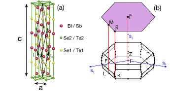
Bismuth dichalcogenides show a rhombohedral crystal structure with a five atom basis that constitute a quintuple layer (QL) –see Figure 1–. The four compounds forming the Bi2Se3 family studied in this work belong to the () crystallographic group. Along the [111] direction each atomic layer contains only one element and is hexagonally compact. The stacking pattern along this direction is …AbCaB… where capital (small) letters indicate the position of Se or Te (Bi or Sb) atoms. Within a QL, interactions among the atoms are strong, while inter–QL bonding is of the weaker vdW kind.
To model the systems we employed the Vienna ab-initio simulation package (VASP) Kresse and Hafner (1993) density functional theory (DFT) code for the atomic relaxations and electronic structure calculations of bulk materials. The SIESTA code Soler et al. (2002), through its implementation in the GREEN package Cerdá et al. (1997), was additionally used for electronic structure calculations of the Bi2Te3–Sb2Te3 heterojunctions. In all the calculations we used the Perdew–Burke–Ernzerhof Perdew et al. (1996) implementation of the generalized gradient approximation (GGA). The semi–empirical pair–potential vdW correction of Grimme Grimme (2006) was used in the atomic relaxations as implemented in the VASP code to correctly account for the weak inter-QL interaction. The spin–orbit coupling was included self–consistently in both VASP Kim et al. (2009) and SIESTA–GREEN Cuadrado and Cerdá (2012) calculations. A 340 eV energy cut–off was employed for the plane wave basis set in VASP calculations, while a double -polarized scheme with confinement energies of 100 meV was used for the numerical atomic orbital basis set in SIESTA. Three–center integrals in SIESTA were computed using an hyperfine mesh cut–off of 1200 Ry, equivalent to a real space grid resolution below 0.05 Å3. Biaxial (uniaxial) strain was taken into account by elongating or contracting lattice parameter () –see Figure 1– and allowing the internal coordinates of the ions to relax. Biaxial and uniaxial strain ( and respectively) of a particular compound with lattice parameters are given by:
| (1) | ||||
where and are the equilibrium values of the in–plane and out–of–plane lattice parameters respectively.
III Uniaxial and Biaxial Tension
III.1 Bulk Materials
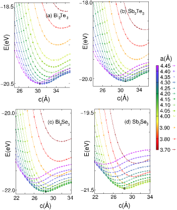
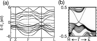
To address the effects of biaxial tension, we first calculated the total energy of the Bi2Se3 family of compounds for different values of the lattice constants using GGA+vdW with the VASP code. In this way, we obtain the relaxed geometry for a fixed value of the in–plane lattice parameter . Figure 2 shows the total energy of Bi2Te3, Sb2Te3, Bi2Se3 and Sb2Se3 for different values of as a function of the out–of–plane lattice constant . The equilibrium lattice parameters and were also calculated, and are given in Table 1. In Figure 3 we show the band structure of fully relaxed Bi2Se3 for both bulk and thin film geometries as a reference. As shown in Figure 2, for compressive in–plane biaxial strains () lattice parameter tends to increase, while for tensile strains () decreases with respect to its equilibrium value. In fact, we can estimate the value of the Poisson ratio from our calculations with the following equation for equibiaxial strained systems Ohring (2001):
| (2) |
| Bi2Te3 | Sb2Te3 | Bi2Se3 | Sb2Se3 | |
|---|---|---|---|---|
| (Å) | 4.40 (4.383) | 4.25 (4.25) | 4.17 (4.138) | 4.04 (-) |
| (Å) | 30.5 (30.487) | 30.9 (30.35) | 28.4 (28.64) | 28.7 (-) |
Fitting the energy minima positions for the curves shown in Figure 2 to eq. 2 we obtain Poisson ratios of 0.30, 0.32, 0.29 and 0.27 for Bi2Te3, Sb2Te3, Bi2Se3 and Sb2Se3 respectively, in agreement with previous calculations Liu et al. (2011); Gao et al. (2016); Koc et al. (2013).
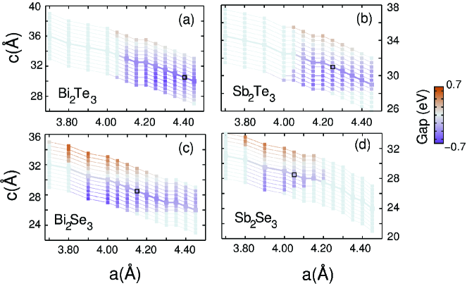
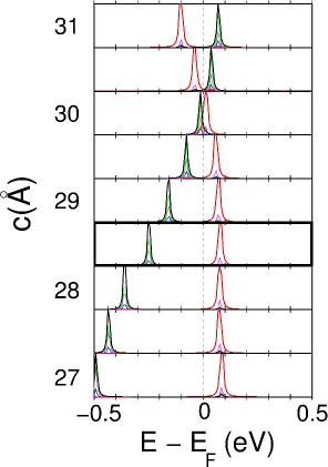
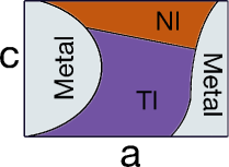
In order to address the combined effects of out–of–plane uniaxial and in–plane biaxial strain, the phase diagram of the Bi2Se3 family of compounds was computed for several points in parameter space . For every pair of values of the lattice constants, we allowed the ionic positions to relax and we calculated the energy spectrum. In this way we can address the combined effect of uniaxial (along the direction) and biaxial strain. The results are summarized in Figure 4 for the four compounds. For a fixed value of , points along vertical lines correspond to increments of 1.5% of uniaxial strain, being the central point of each vertical line the relaxed value of for the given amount of biaxial strain in that line. For the four systems, three distinct phases can be identified: a metallic phase, a topologically trivial insulating phase –normal insulator (NI), with topological invariant 0 – and a topologically non–trivial phase –topological insulator (TI), with topological invariant 1 –. The metallic phase is obtained for large in–plane biaxial strains in any direction. This is due to the fact that a high compressive in–plane strain enhances the bandwidth of the and orbitals in the valence band (VB), which eventually crosses the Fermi level and makes the system metallic. For high tensile in–plane biaxial strains, the conduction band (CB) undergoes an analogous process, leading also to a metallic system. For moderate in–plain strains (below 10% in absolute value) the systems remain insulating. In this range, the topological behavior of these systems is governed by the band inversion between the Se and Bi bands, and a topological phase transition (TPT) can be induced by out–of–plane strain. Starting from an inverted phase, for the bandwidth of the bands is enhanced, which in turn makes the gap bigger at first, until eventually the gap becomes indirect, starts to decrease and at a certain large compressive out–of–plane strain the system becomes metallic again. On the other hand, tensile out–of–plane strain () tends to diminish the gap until it closes when the energies of the Bi and Se bands at the point become equal. Further tensile strain reopens the gap, turning the system into a topologically trivial insulator. Figure 5 shows the behavior of the gap with out–of–plane strain for Bi2Se3 at =4.20 Å. The band gap closing and reopening is evident from the crossing between the Bi and Se bands, which have opposite parity and are responsible for the topological nature of the Bi2Se3 family of compounds Zhang et al. (2009).
For =0, the critical uniaxial strain driving the TPT for Sb2Se3, Bi2Se3 Sb2Te3 and Bi2Te3 is 3%, 6%, 6% and 12% respectively. This trend is in turn related to the crystal structure and the strength of the SOC in each system, being largest in Bi2Te3, smallest in Sb2Se3 and intermediate in Bi2Se3 and Sb2Te3. Note that this values are given for zero biaxial in–plane strain, and the TPT will occur at different values of for (see Figure 4). Other studies have shown similar TPTs for Bi2Se3–like systems under purely uniaxial strain of 6–10% Liu et al. (2014a); Young et al. (2011); Luo et al. (2012); Lysogorskiy et al. (2012); Liu et al. (2014b, 2011); Zhao et al. (2012), which is in good agreement with our results.
Recent studies have revealed the importance of quasiparticle corrections Yazyev et al. (2012); Aguilera et al. (2013) and temperature effects Monserrat and Vanderbilt (2016), which lead to a renormalization of the single-particle bands. However, according to those studies the band inversion persists and the value of the invariant remains unchanged. Therefore, the inclusion of both effects could slightly modify the values of the critical strains, but our results should remain qualitatively correct. In fact, although DFT is known to underestimate band gaps, we find very good agreement between our computed band gaps and experimental data Wyckoff (1964); Black et al. (1957).
The universal phase diagram for the Bi2Se3 family of 3D TIs under the combined effect of uniaxial and biaxial strain is sketched in Figure 6. To our best knowledge, no other previous work has systematically addressed the effects on the topology of combined uniaxial and biaxial strain. Moreover, as the four systems show a positive Poisson ratio, pure compressive biaxial strain induces an expansion in the direction which could, in principle, drive the system into the normal insulating phase. Nevertheless, if no additional uniaxial strain is applied, we find that the four systems undergo a TI to metallic phase transition with both tensile and compressive biaxial strain. The phase diagram we provide for the four compounds can be useful for topological, band and orbital engineering of the Bi2Se3 family of compounds in the fields of straintronics and spintronics.
The Sb2Se3compound
Our results predict unstrained Sb2Se3 to be a topologically non–trivial insulator in the phase. Nevertheless, the region of parameter space in which Sb2Se3 is a TI is small and therefore minor variations of the lattice parameters result in a trivial insulator. Previous calculations have reported this material to be a normal insulator Zhang et al. (2009); Liu et al. (2011); Li et al. (2014) under no strain. Comparing with Refs. Zhang et al., 2009; Li et al., 2014, we obtain slightly smaller lattice constants (=4.04 versus 4.076 Å, =28.7 versus 29.83 Å for Ref. Zhang et al., 2009, and similar values for Ref. Li et al., 2014), probably due to the inclusion of vdW corrections in our calculations. With their lattice constants our calculations also predict Sb2Se3 to be a narrow gap NI –see Figure 4 (d)–. In Ref. Liu et al., 2011 they obtain lattice parameters closer to ours (=4.026 Å, =28.732 Å) within the GGA+vdW approximation, but decide to set the equilibrium (unstrained) configuration at the plain GGA relaxed parameters (without the vdW correction, =4.078 Å, =29.92 Å), yielding again a NI phase. Recent calculations by other group Ryu et al. (2016) estimate smaller values of lattice parameters for rhombohedral Sb2Se3 (=4.004 Å, =28.553 Å) and seem to predict an inverted band structure for antimony selenide –see the curvature of the bands around the point in Figure 2 (d) of Ref. Ryu et al., 2016–, but do not elaborate on its topological nature. Unfortunately, experimental data for Sb2Se3 is only available for its more stable orthorhombic phase (Pnma) Efthimiopoulos et al. (2013). We recently became aware of another work Cao et al. (2016) in which DFT+vdW calculations predict rhombohedral Sb2Se3 to be topologically non–trivial.
III.2 Thin Films
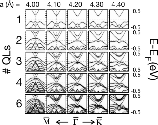
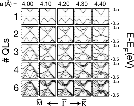
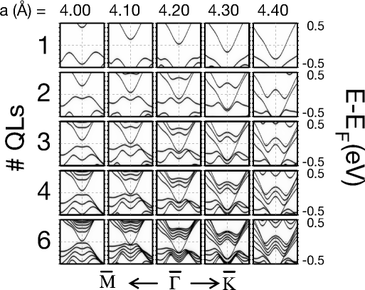
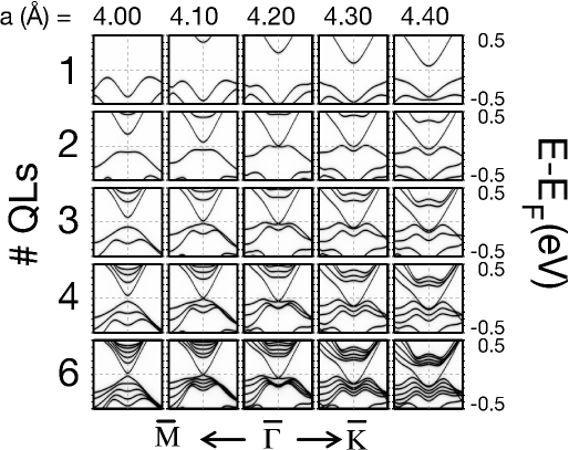
Now we investigate the effect of pure biaxial in–plane strain along with low dimensional effects on thin films of Bi2Se3–like systems. Our starting points are bulk calculations in which, for a fixed amount of biaxial strain, the lattice parameter was allowed to fully relax along with the atomic coordinates. These bulks correspond to the equilibrium systems for each value of the in–plane strain and coincide with the minimum of each curve for fixed in Figure 2, and with the thick lines in Figure 4. Then, slabs of 1, 2, 3, 4 and 6 QL thicknesses were built with the bulk positions and their band dispersions were computed. The results for Bi2Se3 are shown in Figure 7 for the range of lattice parameter in which the bulk system is a TI (see the results for Bi2Te3, Sb2Te3 and Sb2Se3 in the appendix, for the same range of lattice parameters).
The behavior with both compressive and tensile biaxial strain of Bi2Se3 thin films is in clear analogy with the bulk behavior. Nevertheless, they show distinct features induced by strain. Under compressive biaxial strain the size of the Bi2Se3 bulk gap acquires a smaller value than that of the unstrained system, and therefore the penetration depth of the surface states is enlarged and a larger number of layers is needed to close the hybridization gap. Moreover, the ”M”–shaped feature in the VB around the point is smoothed out and consequently the linear dispersion of the TSS is extended to a larger energy region in the VB. On the other hand, applying tensile biaxial strain also tends to close the bulk gap, but the ”M”–shaped feature becomes more pronounced and hence the DP in the films is shifted inside the VB (see the 6 QL series in Figure 7). A sharp enough ”M”–shaped VB detaches the DP from the Fermi level and consequently induces an –type doping of the surface states. This result explains the shift in the DP observed in Ref. [Zhao et al., 2012], as well as the different behavior, gap opening or -doping, observed at the grain boundaries in Bi2Se3 films, in regions under compressive or tensile strain, respectively Liu et al. (2014a).
Moreover, a small decrease in the Fermi velocity with tensile strain is also apparent. The penetration depth of the TSS also varies with strain, and the closer in the phase diagram to the critical Metal–TI lines the more QLs are needed to close the hybridization gap (see for instance the 2 QL series in Figure 7, in which compressive or tensile biaxial strain takes the system closer to a critical line in the phase diagram, and the TSS are gapped but for ), in agreement with the results displayed in Ref. [Liu et al., 2014a]. Higher compressive biaxial strain drives the thin films into a metallic state due to the upward shift in energy of the valence band maximum (see for example Figure 16 in the appendix), while for a critical tensile biaxial strain the bulk–like CB crosses the Fermi level and the thin films become metallic again (see Figure 18).
Strain can therefore turn the Bi2Se3 family of compounds insulating or metallic, and allows for engineering of the gap, the orbital character of the bands, the Fermi velocity, DP energy and thus also the doping of the TSSs. The table–like figures for the four systems are displayed so that they can be used for determining what kind of band dispersion is expected when a bismuth dichalcogenide of a certain thickness is grown on a substrate with a particular lattice parameter.
IV Strained Heterojunctions
When two distinct TIs are faced to one another, an interesting problem arises. If both materials belong to the same topological class, no interface state is guaranteed by the bulk–to–boundary correspondence, as the change in topological invariant is zero. Therefore, a topological surface state can be annihilated by placing another TI on top, even if both bulk gaps align in a straddling gap configuration. Still, topologically trivial interface states may arise regardless of the topological invariants. Moreover, in broken gap heterojunctions (without a common gap) no topologically protected interface state may appear since the system will no longer be an insulator. In this section we will study interfaces of Bi2Te3 and Sb2Te3 both in superlattices and in slab geometry. Among the four members of the Bi2Se3 family of compounds, we have chosen these two so that the difference in electronegativity, , between the A and B elements in the A2B3 compounds is as small as possible, in order to obtain a straddling gap at the heterojunction and minimize the band bending along the system. Table 2 shows the Pauling and Allen electronegativities ( and ) for Bi, Sb, Te and Se. The first two elements have an almost equal value of the electronegativity –in fact BiSb while BiSb–. On the other hand, Se and Te show a bigger difference in their values. Opposite doping for Se- and Te-based materials is expected, and we have additionally calculated Bi2Se3/Bi2Te3 heterojunctions which exhibit a broken gap alignment, thus leading to a metallic phase where the invariant is ill-defined and no topological interface states can exist.
| Bi | Sb | Te | Se | |
|---|---|---|---|---|
| Pauling (1932) | 2.02 | 2.05 | 2.1 | 2.55 |
| Allen (1989) | 2.01 | 1.984 | 2.158 | 2.434 |

IV.1 TI/TI interfaces
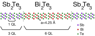
We have chosen Sb2Te3/Bi2Te3/Sb2Te3 trilayers with equal number of QLs of Sb2Te3 at both sides so that inversion symmetry is preserved, making the analysis simpler, as both interfaces will be equivalent. We calculated -Sb2Te3/-Bi2Te3/-Sb2Te3 trilayers, where and are the number of QLs of Sb2Te3 and Bi2Te3 respectively. In the superlattice geometry, due to periodic boundary conditions, the trilayer turns into a 2-Sb2Te3/-Bi2Te3 structure repeated in the [111] direction. We still call it a -Sb2Te3/-Bi2Te3/-Sb2Te3 superlattice to emphasize the centrosymmetric nature of the system. We fixed =6, for which the surface–surface interaction in Bi2Te3 is negligible and a gapless Dirac cone (DC) develops at the surface –see Fig. 9(a)–, while the number of Sb2Te3 QLs at both sides is varied from =1 to 3. The AbCaB stacking sequence of the pristine subsystems is preserved along the interfaces and in the superlattices in order to preserve inversion symmetry. The rotation axis and the three vertical mirror planes of the pristine systems are also preserved in the heterojunction. We fix the in–plane lattice vector to that of Sb2Te3 in equilibrium, =4.25 Å, and the lattice parameter for each subsystem is set to its relaxed value for fixed to the aforementioned value, that is 30.9 Å for Sb2Te3 and 32.0 Å for Bi2Te3 (see Fig. 2). The ionic coordinates within each subsystem are fixed to their relaxed bulk values, and the vdW gap between Sb2Te3 and Bi2Te3 is taken as the average vdW gap between both subsystems. This setup could correspond to a 6 QL thick Bi2Te3 slab grown on a –QL Sb2Te3 substrate, and another –QL Sb2Te3 thin film grown on top of it. Figure 8 depicts the geometry for the =3 case. According to the phase diagram calculated in Fig. 4, both the Sb2Te3 and Bi2Te3 subsystems show an inverted gap in the bulk. This means that the existence of an interface state is not guaranteed, since the change in the invariant across the interface is zero as both materials are topological insulators.
We start by analyzing the electronic structure of the isolated subsystems, depicted in Figure 9. Bi2Te3 under small biaxial strain remains a TI, and so it develops surface states when truncated in the [111] direction. For a 6 QL slab (as shown in the figure), surface–surface interaction is already negligible and the linearly dispersive DCs at the point emerge. In contrast with Bi2Se3 or Sb2Te3, the DP of the Bi2Te3 surfaces is not at the Fermi level and lies below the VB maximum. This is in agreement with previous results Zhang et al. (2009), and can be attributed to the larger curvature of the VB along the – direction. Sb2Te3 in this system presents neither uniaxial nor biaxial strain, and it is therefore also in the topologically non–trivial phase. In Figure 9 the electronic structure of unstrained 1, 2, 3, 4 and 6 QL thick Sb2Te3 films is also shown –panels (b) to (f)–. Antimony telluride presents a topological surface state being the DP at the Fermi level for 6 QLs. The penetration depth is 2 QLs, so that a gap opens in thin films of less than 5 QLs due to surface–surface hybridization.
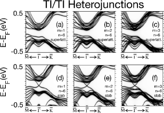
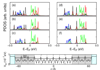
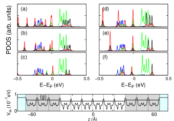
The band structures of the periodic superlattices are shown in Figure 10 (a) to (c) for =1, 2 and 3, and those corresponding to the trilayer slabs in Figure 10 (d) to (f). The former –(a), (b) and (c)– present a band gap of 0.1 eV, being the VB (CB) offset of 0.1 (0.05) eV between both subsystems, with the VB (CB) of Sb2Te3 lying at a higher energy. The small band staggering at the heterojunction can be attributed to the small deviation in the values of the electronegativity for Bi and Sb. Figs. 11 (a), (b) and (c) represent the atomic orbital decomposed partial density of states (PDOS) at in the energy region displayed in Fig. 10. They evidence the band inversion in both Sb2Te3 and Bi2Te3 slabs and the similar band alignment for the three superlattices, =1, 2 and 3. The top of the VB is dominated by Sb and Bi orbitals with positive parity, being the former at higher energy, while the Te orbitals with negative parity are located at the bottom of the CB region. The interaction between the CB Te orbitals of both compounds is weak, particularly for the wider superlattices. Hence, in the superlattice both subsystems present an inverted band structure.
The bulk–to–boundary correspondence predicts no topologically protected interface state at the junction, and although trivial interface states could develop, our results show that this is not the case. We therefore conclude that this Sb2Te3/Bi2Te3 heterojunction is insulating with no interface states whatsoever, but will develop surface states when truncated. This is proved in the thin film geometry –Figure 10 (d),(e) and (f)–, where surface states that span the whole bulk band gap appear at both ends. The DP of these TSSs is pinned at the Fermi level irrespective of the thickness of the Sb2Te3 layers. In fact, even for the =1 and 2 for which the thickness of the Sb2Te3 subsystem is below the penetration depth of the surface states -see Figure 9 (b) and (c)-, there is no energy gap and the spectrum of the trilayer slab still exhibits a semimetallic character. The corresponding atomic orbital PDOS are shown in Fig. 11 (d) to (f). The three trilayers exhibit a sharp peak at , associated with the TSSs. They have a predominant contribution of the Sb2Te3 orbitals, mostly of Sb .
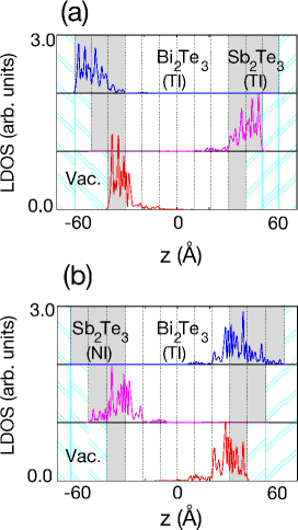
This orbital contribution is consistent with the TSS localization shown in Figure 12 (a), for the three different slabs. The surface state is strongly confined in the Sb2Te3 subsystem, with a penetration depth of 2 QLs, although for the =1 case the state strongly localizes at the surface-most QL. Fig. 11 (g) displays the 2D averaged Hartree potential profiles –including the ionic contribution– along the [0001] direction for the =3 slab. It reflects the chemical difference between both Sb2Te3 and Bi2Te3 compounds and the potentials are almost identical for the finite trilayers and the superlattice (not shown), differing only on the potential step at the surface of the slab. Therefore, our results corroborate the fact that unstrained Sb2Te3 is a TI even for ultrathin films, and support the idea that the TI/TI Sb2Te3-Bi2Te3 heterojunction behaves as a homogeneous TI and does not confine neither topological nor trivial states at the interface.
IV.2 NI/TI interfaces
Now we will discuss the effect of applying uniaxial tensile strain to Sb2Te3 in the system presented in the previous subsection. The systems considered are again -Sb2Te3/-Bi2Te3/-Sb2Te3 trilayers in either a slab geometry (thin film) or a superlattice. The in–plane lattice parameter is again fixed to =4.25 Å and is set to 32.0 Å for Bi2Te3, but now the Sb2Te3 subsystem is expanded to =34.0 Å, corresponding to an uniaxial tensile strain of -10%. According to the phase diagram shown in Figure 4, Sb2Te3 will now be in a normal insulating phase, so that at the interface of Sb2Te3 and Bi2Te3 the topological invariant will increase from 0 to 1. The TPT on Sb2Te3 can be induced by external uniaxial tensile strain or via the chemical intercalation of zerovalent non–magnetic metals in the vdW gaps Koski et al. (2012) as stated in a previous section.
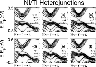
The electronic structure of the different isolated constituents is shown in Figure 9 (a) and (g) to (k). Sb2Te3 under such out–of–plane strain shows no band inversion in the bulk, and this is reflected in the thin film electronic structure. In contrast with the previously analyzed systems, Sb2Te3 now shows no surface state since it is in the NI phase. The gap is of 0.4 eV for the 1 QL slab –Figure 9 (g)–and decreases down to 0.2 eV for the 6 QL thin film –Figure 9 (k)–. On the other hand, the 6 QL Bi2Te3 slab under purely biaxial strain is a TI which develops TSSs with no gap, and its DP lies below the Fermi level –Figure 9 (a)–. When the two subsystems are brought together, the bulk–to–boundary correspondence dictates that topologically protected interface states must develop in the gap. The band structures of the junctions are shown in Figure 13 (a) to (f).
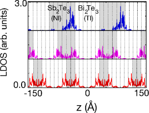
For periodic boundary conditions –panels (a) to (c) of Figure 13–, and in contrast to the TI/TI superlattices analyzed in subsection IV.1, a topological interface state (TIS) develops that spans the bulk band gap. Unexpectedly, the interface topological state localizes in the normal insulator Sb2Te3 (see Figure 14), as opposed to TSSs, which always localize in the topological insulator. In this heterojunction a hybridization gap opens in the spectrum for thicknesses of the –Sb2Te3 layer below =2 QLs –Figure 13 (b)– since the two opposed interfaces are closer than twice the penetration depth of the TISs. The TISs show no doping in contrast with the TSS of 6 QL Bi2Te3 –see Figure 13 (f)–, opening a new way of tuning the DP energy of the topological states.
To understand the fundamental difference between the TI/TI and NI/TI heterojunctions, we analyze the atomic orbital PDOS at in Figs. 11 and 15. While the Bi2Te3 shows band inversion in both cases, the Sb2Te3 subsystem exhibits opposite traits in the two different sets of heterojunctions. In the TI/TI systems, as discussed previously, there is band inversion, while in the NI/TI there is not. In the NI/TI case the Te orbital of the Sb2Te3 with negative parity occupies the top of the VB region, while the Sb orbital with positive parity is located at the CB just above the Te derived bands of Bi2Te3. Therefore, the Sb2Te3 remains in the trivial state. Nevertheless, the topological interface states are mainly formed from the orbitals closest to the energy gap, namely from the Te orbitals of Sb2Te3. This feature explains why the TISs are located predominantly in the non-topological slab. Furthermore, due to their spatial localization, there is a strong interaction between the TISs at both interfaces for =1 and 2, and a gap opens up.
For the trilayer slab configurations shown in panels (d) to (f) of Figure 13, the system shows a common bulk gap of 0.15 eV and a gapless interface state with the DP at the Fermi level. This topological interface state is also undoped and develops irrespective of the thickness of the non-topological Sb2Te3 layers, and analogously to the emergent TISs in the SLs, it is not strictly localized at the interface. Instead, the state at the gap is confined in the Sb2Te3 subsystem, with more weight at the interfacemost QL of Sb2Te3, but exceeding the expected 2 QL penetration depth of the TSSs in an isolated Bi2Te3 slab –see Figure 12 (b)–. Moreover, the orbital distribution in the VB and CB, and hence that of the TIS, is similar in the NI/TI superlattices and trilayers (see Fig. 15). The main difference between the superlattice and the trilayer TISs lies in the lack of interaction in the trilayer geometry due to the localization in the Sb2Te3 subsystem. Thus, all the trilayers remain semimetallic. On the other hand, only minor differences between the averaged Hartree potential of NI/TI and TI/TI heterostructures of equivalent TI/TI geometry –see Fig. 11 (g) and Fig. 15– are observed.
Our findings are in agreement with previous results Zhang et al. (2012); Men’shov et al. (2014); Brahlek et al. (2016); Menshchikova et al. (2013) in which similar TISs with large penetration depths appear in NI/TI junctions localized in the NI. We additionally checked that in NI/TI/NI heterojunctions of -Sb2Te3/-Bi2Te3/-Sb2Te3 with as low as 1 QL, the TISs are always gapless in slab configuration, and remain gapless in superlattice geometries as long as . Note that Bi2Te3 here is the TI, and 1 QL Bi2Te3 thin films show a relatively large Dirac gap due to surface–surface hybridization. Therefore, capping Bi2Te3 with uniaxially strained Sb2Te3 leads to a closing of the Dirac gap in the topological states, since the latter localizes in the normal insulating Sb2Te3. In addition, although the development of TISs in NI/TI junctions is dictated by topology, their spatial location is determined by the orbitals dominating the edges of the valence and conduction band of the heterostructures, and thus by the relative alignment of the bands of both subsystems.
V Summary and conclusions
We have shown the combined effects of uniaxial and biaxial strain on Bi2Te3, Sb2Te3, Bi2Se3 and Sb2Se3, both in bulk and slab geometries. A phase diagram for the four systems was computed and analyzed, demonstrating that topological phase transitions, either to a metal or to a trivial insulator, can occur for different combinations of both kinds of strains, and a universal behavior was found for the four compounds. We showed how strain can engineer the DP energy, the Fermi velocity, the metallic character and the topology of the four compounds, thus offering a wide tunability regarding straintronics. We have also calculated the electronic structure of Sb2Te3/Bi2Te3/Sb2Te3 trilayers, in which Sb2Te3 was driven into the topologically trivial insulating regime by applying uniaxial strain. For the TI/TI systems no trivial nor topological interface state is found, and the superlattice shows a straddling gap of 0.1 eV. In the NI/TI heterojunctions, topologically protected interface states are predicted and characterized. Since the TIS spatial location is determined by the relative band alignment of the two compounds forming the heterostructures, we find TISs to localize in the NI both in slab configurations and periodic superlattices, thus opening a route to closing hybridization gaps in topological states of ultrathin films of the Bi2Se3 family by capping the system with NI layers. Our results for the NI/TI heterojunctions also indicate a way to avoid interactions of the topological states with undesired ambient impurities while preserving the bulk band gap of the system, and thus maintaining the topological protection of the states. Uniaxial strain on the Sb2Te3 subsystem can additionally turn the interface conducting channel on or off, thus the system hosts a switchable topological interface state irrespective of the thickness of the TI layer.
Acknowledgments
This work has been supported by the Spanish Ministry of Economy and Competitiveness through Grant MINECO/FEDER No. MAT2015-66888-C3-1R. We acknowledge the use of computational resources of CESGA, Red Española de Supercomputación (RES) and the i2BASQUE academic network.
References
- Fu et al. (2007) L. Fu, C. L. Kane, and E. J. Mele, Phys. Rev. Lett. 98, 106803 (2007).
- Roy (2009) R. Roy, Phys. Rev. B 79, 195322 (2009).
- Kane and Mele (2005) C. L. Kane and E. J. Mele, Phys. Rev. Lett. 95, 146802 (2005).
- Hasan and Kane (2010) M. Z. Hasan and C. L. Kane, Reviews of Modern Physics 82, 3045 (2010).
- Zhang et al. (2009) H. Zhang, C.-X. Liu, X.-L. Qi, X. Dai, Z. Fang, and S.-C. Zhang, Nature Physics 5, 438 (2009).
- Basak et al. (2011) S. Basak, H. Lin, L. A. Wray, S.-Y. Xu, L. Fu, M. Z. Hasan, and A. Bansil, Phys. Rev. B 84, 121401 (2011).
- Aramberri et al. (2015) H. Aramberri, J. I. Cerdá, and M. C. Muñoz, Nano Letters 15, 3840 (2015).
- Liu et al. (2014a) Y. Liu, Y. Y. Li, S. Rajput, D. Gilks, L. Lari, P. L. Galindo, M. Weinert, V. K. Lazarov, and L. Li, Nature Physics 10, 294 (2014a).
- Young et al. (2011) S. M. Young, S. Chowdhury, E. J. Walter, E. J. Mele, C. L. Kane, and A. M. Rappe, Phys. Rev. B 84, 085106 (2011).
- Luo et al. (2012) X. Luo, M. B. Sullivan, and S. Y. Quek, Phys. Rev. B 86, 184111 (2012).
- Lysogorskiy et al. (2012) Y. V. Lysogorskiy, A. G. Kijamov, O. V. Nedopekin, and D. A. Tayurskii, Journal of Physics: Conference Series 394, 012022 (2012).
- Liu et al. (2014b) J. Liu, Y. Xu, J. Wu, B.-L. Gu, S. B. Zhang, and W. Duan, Acta Crystallographica Section C 70, 118 (2014b).
- Liu et al. (2011) W. Liu, X. Peng, C. Tang, L. Sun, K. Zhang, and J. Zhong, Phys. Rev. B 84, 245105 (2011).
- Zhao et al. (2012) L. Zhao, J. Liu, P. Tang, and W. Duan, Applied Physics Letters 100, 131602 (2012).
- Koski et al. (2012) K. J. Koski, C. D. Wessells, B. W. Reed, J. J. Cha, D. Kong, and Y. Cui, Journal of the American Chemical Society 134, 13773 (2012), pMID: 22830589.
- Kim et al. (2016) T.-H. Kim, K. Jeong, B. C. Park, H. Choi, S. H. Park, S. Jung, J. Park, K.-H. Jeong, J. W. Kim, J. H. Kim, and M.-H. Cho, Nanoscale 8, 741 (2016).
- Kresse and Hafner (1993) G. Kresse and J. Hafner, Phys. Rev. B 48, 13115 (1993).
- Soler et al. (2002) J. M. Soler, E. Artacho, J. D. Gale, A. García, J. Junquera, P. Ordejón, and D. Sánchez-Portal, Journal of Physics: Condensed Matter 14, 2745 (2002).
- Cerdá et al. (1997) J. I. Cerdá, M. A. Van Hove, P. Sautet, and M. Salmeron, Phys. Rev. B 56, 15885 (1997).
- Perdew et al. (1996) J. P. Perdew, K. Burke, and M. Ernzerhof, Phys. Rev. Lett. 77, 3865 (1996).
- Grimme (2006) S. Grimme, Journal of Computational Chemistry 27, 1787 (2006).
- Kim et al. (2009) Y.-S. Kim, K. Hummer, and G. Kresse, Phys. Rev. B 80, 035203 (2009).
- Cuadrado and Cerdá (2012) R. Cuadrado and J. I. Cerdá, Journal of Physics: Condensed Matter 24, 086005 (2012).
- Ohring (2001) M. Ohring, Materials science of thin films (Academic press, 2001).
- Wyckoff (1964) R. W. G. Wyckoff, Crystal structures, Vol. 2 (New York: Wiley, 1964).
- Gao et al. (2016) X. Gao, M. Zhou, Y. Cheng, and G. Ji, Philosophical Magazine , 1 (2016).
- Koc et al. (2013) H. Koc, A. M. Mamedov, and E. Ozbay, in Applications of Ferroelectric and Workshop on the Piezoresponse Force Microscopy (ISAF/PFM), 2013 IEEE International Symposium on the (IEEE, 2013) pp. 41–44.
- Yazyev et al. (2012) O. V. Yazyev, E. Kioupakis, J. E. Moore, and S. G. Louie, Phys. Rev. B 85, 161101 (2012).
- Aguilera et al. (2013) I. Aguilera, C. Friedrich, G. Bihlmayer, and S. Blügel, Phys. Rev. B 88, 045206 (2013).
- Monserrat and Vanderbilt (2016) B. Monserrat and D. Vanderbilt, Phys. Rev. Lett. 117, 226801 (2016).
- Black et al. (1957) J. Black, E. M. Conwell, L. Seigle, and C. W. Spencer, Journal of Physics and Chemistry of Solids 2, 240 (1957).
- Li et al. (2014) W. Li, X.-Y. Wei, J.-X. Zhu, C. S. Ting, and Y. Chen, Phys. Rev. B 89, 035101 (2014).
- Ryu et al. (2016) B. Ryu, B.-S. Kim, J. E. Lee, S.-J. Joo, B.-K. Min, H. Lee, S. Park, and M.-W. Oh, Journal of the Korean Physical Society 68, 115 (2016).
- Efthimiopoulos et al. (2013) I. Efthimiopoulos, J. Zhang, M. Kucway, C. Park, R. C. Ewing, and Y. Wang, Scientific reports 3 (2013).
- Cao et al. (2016) G. Cao, H. Liu, J. Liang, L. Cheng, D. Fan, and Z. Zhang, arXiv preprint:1607.05911 (2016), arXiv:1607.05911 [cond-mat] .
- Pauling (1932) L. Pauling, Journal of the American Chemical Society 54, 3570 (1932).
- Allen (1989) L. C. Allen, Journal of the American Chemical Society 111, 9003 (1989).
- Zhang et al. (2012) Q. Zhang, Z. Zhang, Z. Zhu, U. Schwingenschlögl, and Y. Cui, ACS nano 6, 2345 (2012).
- Men’shov et al. (2014) V. N. Men’shov, V. V. Tugushev, T. V. Menshchikova, S. V. Eremeev, P. M. Echenique, and E. V. Chulkov, Journal of Physics: Condensed Matter 26, 485003 (2014).
- Brahlek et al. (2016) M. J. Brahlek, N. Koirala, J. Liu, T. I. Yusufaly, M. Salehi, M.-G. Han, Y. Zhu, D. Vanderbilt, and S. Oh, Phys. Rev. B 93, 125416 (2016).
- Menshchikova et al. (2013) T. V. Menshchikova, M. M. Otrokov, S. S. Tsirkin, D. A. Samorokov, V. V. Bebneva, A. Ernst, V. M. Kuznetsov, and E. V. Chulkov, Nano Letters 13, 6064 (2013), pMID: 24274792, http://dx.doi.org/10.1021/nl403312y .
*
Appendix A Band dispersion tables for Bi2Te3, Sb2Te3 and Sb2Se3
