Optically Thin Metallic Films for High-radiative-efficiency Plasmonics
Abstract
Plasmonics enables deep-subwavelength concentration of light and has become important for fundamental studies as well as real-life applications. Two major existing platforms of plasmonics are metallic nanoparticles and metallic films. Metallic nanoparticles allow efficient coupling to far field radiation, yet their synthesis typically leads to poor material quality. Metallic films offer substantially higher quality materials, but their coupling to radiation is typically jeopardized due to the large momentum mismatch with free space. Here, we propose and theoretically investigate optically thin metallic films as an ideal platform for high-radiative-efficiency plasmonics. For far-field scattering, adding a thin high-quality metallic substrate enables a higher quality factor while maintaining the localization and tunability that the nanoparticle provides. For near-field spontaneous emission, a thin metallic substrate, of high quality or not, greatly improves the field overlap between the emitter environment and propagating surface plasmons, enabling high-Purcell (total enhancement > ), high-quantum-yield (> 50%) spontaneous emission, even as the gap size vanishes (35 nm). The enhancement has almost spatially independent efficiency and does not suffer from quenching effects that commonly exist in previous structures.
keywords:
nanoparticles, optical nanoantennas, radiative efficiency, metallic thin film, light scattering, spontaneous emissionPhysics Department and Solid State Institute, Technion, Haifa 320000, Israel
Ohmic loss in metals is the most critical restriction for plasmonics 1. The restriction can be characterized by the radiative efficiency , defined as the ratio between the radiative decay rate and the total decay rate, i.e., . Two major existing platforms of plasmonics are metallic nanoparticles2, 3, 4, 5, 6, 7 and metallic films 8, 9, 10, 11; they both face their own restrictions for achieving a high . A major problem regarding nanoparticles is their poor material qualities due to the amorphous structures that arise from the colloidal synthesis processes. In comparison, single- or poly-crystalline metallic films fabricated via temperature-controlled sputtering or epitaxial growth can achieve much higher material qualities and much lower material losses, but their coupling to radiation is typically jeopardized due to the large momentum mismatch with free space. When the two platforms are combined, the radiation of nanoparticles is also at risk of being quenched by a bulk nearby metallic film. These restrictions lead to compromises between and other mode properties, such as quality factor () and mode volume 12, 13, 14 ().
For plasmonic light scattering, it is often desirable to achieve high radiative efficiencies and high simultaneously. In biomedical sensing 15, 16, 17, 18, for example, a high Q is required for high spectral resolution, while a high radiative efficiency (stronger scattering) is needed for high signal-to-noise ratio (SNR). Meanwhile, transparent displays19, 20, 21 based on resonant scattering demand high for high transparency and high radiative efficiencies for high brightness. However, it is very challenging to achieve both goals at the same time. First, , , and are all bounded from above as functions of the permittivities of materials 22, 23, 24, 25, primarily due to the intrinsic material loss. Second, there exists a fundamental physical contradiction between the two requirements: higher radiative efficiencies require higher radiative decay rates, which necessarily reduce the total quality factors.
For plasmon-enhanced emission26, 27, 28, 29, 30, 31, 32, another trade-off exists between achieving high quantum yield (QY) and large Purcell 33 factors, even though both are typically desired. The key to achieving high spontaneous emission enhancement over a broad band 32, 34 using plasmonics is to achieve small s. However, as decreases, absorptive decay rates (proportional to 35) dominate over radiative decay rates (proportional to 35), triggering a drastic drop in QY 36, 31, 37. Recently, much effort has been made to enhance spontaneous emission using gap plasmons 38, 39, 28, 40, 29, 30, 36, created via the confinement of light within the dielectric gap between nanoparticles and an optically thick metallic substrate. Compared with other types of resonances, the gap plasmon resonance achieves high total enhancement 30 as it offers more reliable control of the dielectric gap thinness. However, these gap plasmon resonances cannot circumvent the tradeoff between QY and . For example, when the gap size is reduced to 5 nm or smaller for a nanocube, despite a higher total decay rate, the efficiency (defined as the sum of photon and plasmon radiative efficiency 30, 29, 36) drops below 20% 30, 36. Moreover, the efficiency is strongly dependent on the location of emitters. QY reaches maximum if the emitter is placed at the center of the gap but decreases immensely when the emitter is in the proximity of the metal 30.
Here, we propose and theoretically demonstrate that an optically thin metallic film makes an ideal platform for high-radiative-efficiency plasmonics via two examples: high- scattering and enhanced emission. For scattering, a high-quality thin metallic film facilitates a high-, high-radiative-efficiency Mie plasmon resonance, whose exceeds the quasistatic of the nanoparticle material. For enhanced emission, gap plasmons can still be well supported and are better mode overlapped with external radiation using an optically-thin metallic substrate. A high-Purcell (total enhancement > ), spatially-independent-efficiency (>50%) spontaneous emission enhancement can be achieved with vanishing gap size (35 nm), even if the substrate has the same material properties as the nanoparticles. Our platform can also be extended to other applications (for example, nonlinear frequency generation and multiplexing), because of the enhanced efficiencies of high-order plasmonic modes. Moreover, the ratio between photon and plasmon radiation can be easily tailored by altering the shape of the nanoparticles, making this platform versatile for both fluorescence 30, 29, 31 and plasmon circuits 41, 42, 43, 44.
Below we show that in plasmonic optical scattering, the quasistatic of a deep subwavelength nanoparticles can be exceeded with the help of an optically thin high-quality metal film, while maintaining considerably high radiative efficiencies , which is also known as the scattering quantum yield 15 or the albedo 45 in scattering problems. For a subwavelength scattering process, based on temporal coupled-mode theory46, 47, the radiative efficiency and the total quality factor for a single resonance are given by
| (1) | |||||
| (2) |
where is the resonant frequency, is the total decay rate, and is the extinction cross-section. As is mostly dictated by material absorption 22, 23, to get a high , one has to increase . This in turn spoils the quality factor (Eq. 2), which reveals the trade-off between and , as we described previously. Because simultaneously achieving a high and a high is important for many applications, like biomedical sensing15, 16, 17, 18 and transparent displays19, 20, 21, we define the figure of merit (FOM) for scattering as
| (3) |
It follows that this FOM reduces to the quasistatic quality factor 22
| (4) |
which only depends on the material property of the nanoparticle. Here, and are real and imaginary parts of the complex permittivity. For subwavelength metallic nanoparticles (dimension ), their plasmon properties are typically dominated by quasistatic considerations22 and thus the approximation holds, which also indicates that the material loss inside the metallic nanoparticle cannot be further reduced. Therefore, our strategy is to squeeze parts of the resonant mode into a high-quality metallic film8, 9 with much lower loss, while maintaining efficient radiation rates.
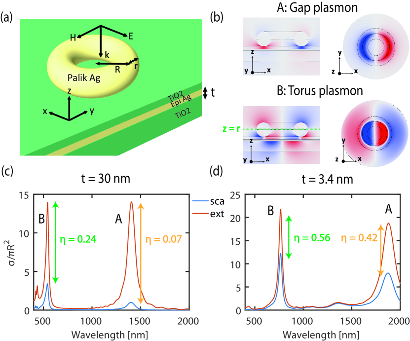
As an example, we investigate a silver torus 48, 49, 50, 51 scatterer, sitting on top of a TiO2-Ag-TiO2 multifilm, whose structural geometry is shown in Fig. 1(a). The permittivities of the silver film and the torus are obtained from Wu8 and Palik52, respectively; the former has substantially lower loss since it is assumed to be made epitaxially. The permittivity of amorphous TiO2 (refractive index 2.5 in the visible and near-infrared spectra) is from Kim 53. The material absorption in TiO2 is negligible compared with the absorption in silver, as is several orders of magnitude lower than that of within the wavelength range of interest. Thus the absorption in TiO2 is not considered in the calculation. The ambient index of refraction is (near the refractive index of water, tissue fluids, and various polymers). If the structure is probed with normally incident plane waves, only the ( is the azimuthal index of the modes since the structure is axially-symmetric) modes of the structure can be excited 35. Fig. 1(b) shows the mode profiles of the two resonances in this structure. Resonance A is a gap plasmon resonance 39 whose field is mostly confined in the upper TiO2 layer. Resonance B corresponds to the torus (Mie) plasmon resonance 54, given that it maintains a nodal line [green dashed line in Fig. 1(b)] along ( is the minor radius of the torus), which is a feature of the torus resonance in free space 48, 49, 50, 51. Fig. 1(c) and (d) compare and of the torus when the silver layer in the multifilm is optically thick ( = 30 nm) or thin ( = 3.4 nm). For both resonances, the radiative efficiency in the thin-film case is much higher than that in the thick-film case. Moreover, when the torus moves away from the multifilm, the response of resonances is very different for the thin film case from that for the thick film, as shown in Fig. S1. We now focus on the Mie resonance B for high- scattering as most of its entire radiation (photon and plasmon combined) goes into the far field (photon). We will return to the gap plasmon resonance A later for enhanced emission applications.
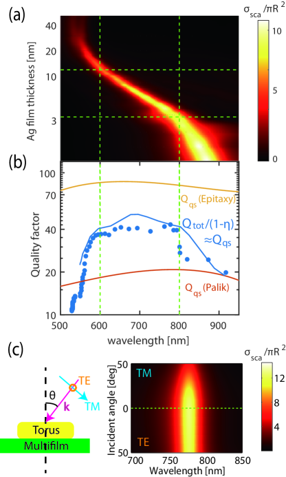
By changing from 0 nm to 50 nm while keeping other parameters unchanged ( nm corresponds to a single 25-nm TiO2 layer), we are able to track the torus plasmon resonance B and evaluate its FOM, as shown in Fig. 2. As increases, the resonance blueshifts, along with a reduced linewidth [Fig. 2(a)]. In Fig. 2(b), we compare the FOM in our structure to the quasistatic limit for different materials in the system: the Palik silver52 that is used for the torus and the epitaxial silver that is used for the substrate8 (FOM and are directly comparable, see Eqs. 3 and 4). There exists a plateau of higher FOM at nm. At these thicknesses, the multifilm still has very high transmission > 80% (Fig. S2). The FOM of the torus plasmon resonance exceeds and becomes twice as high as the of the torus material (Palik 52). When the silver layer is either too thin (< 3 nm) or too thick (> 20 nm), the FOM drops considerably and FOM, the quasistatic quality factor of the torus material. Fig. 2(c) shows that the high FOM can be maintained for both polarizations over a wide range of incident angles.
The increased quality factor is the result of effective mode squeezing that only occurs in thin silver films – an effect we qualitatively demonstrate in Fig. S3 of the Supporting Information. The mode squeezing mechanism can be quantitatively demonstrated by calculating the energy density integral of the eigenmode. The energy density in lossy media is generally defined as 55, where and are real and imaginary parts of permittivity respectively, and is the damping of the metal. We adopt rad/s for the Palik silver and rad/s for the epitaxial silver to best match the tabulated data. Since the metallic objects (Palik silver torus and epitaxial silver film) dominate the absorption loss in this system, we define the energy concentration coefficients in the torus and the film as
| (5) | |||
| (6) |
Thus, the of the system can be estimated as
| (7) |
As shown in Fig. 2(b), the of the system, calculated from the scattering (blue dots) and eigenmode (blue curve) simulations respectively, match each other well. Our calculation shows the high energy concentration in the film only happens when the film is optically thin (see Fig. S4). Near the maximum of the (wavelength 700 nm, silver film thickness 7 nm), the energy concentrated in the film is three times higher than that in the torus (). We also note that the curves of the two materials are quite flat within the wavelength of interest. Thus, it is the effective mode squeezing into a high-quality film, rather than the dispersion of an individual material, that contributes to the improved quality factor of the system.
The aforementioned enhanced is different from the linewidth narrowing that is based on the interference between multiple resonances 2. For coupled resonances, as the trace of the full Hamiltonian is conserved, the linewidth reduction of one resonance necessarily implies the broadening of the others’. This coupling also typically renders the spectrum Fano-like with dark states in the middle of the spectrum 56. In contrast, here the linewidth reduction is realized via effectively squeezing a single Mie plasmon mode into an optically-thin metallic film. Scattering spectrum is kept single-Lorentzian, which is favorable for many applications 16, 17, 18, 19, 21 as it maintains a high resolution and SNR. Moreover, as the resonance for scattering uses the Mie plasmon and the ambient environment is the perturbed free space, most of the reradiated energy goes into the far field with weak plasmon excitation (see supporting information). We also note that optically thin metallic films are not restricted to high- applications shown above. Applications based on broadband strong scattering (like solar cells requiring longer optical path) can also be implemented on this platform, utilizing its high radiative efficiency.
Antennas work equally well as receivers and as transmitters; in the context of nanoparticles, the radiative efficiency is equally important, whether nanoparticles are used to scatter light from the far field or serve as external cavities to enhance spontaneous emission in the near field. The quantum yield (QY) of an emitter (whose total decay rate is in free space) enhanced by a plasmonic nanoparticle can be approximated as32 under the assumption that the decay rate is dominated by the plasmonic resonance (note we use and to denote the emission and scattering processes respectively). Here, , is the radiative decay rate of the emitter not coupled to the cavity, is the modified emission rate in the presence of the cavity, and are radiative and absorptive decay rates of the cavity respectively, is the intrinsic nonradiative decay rate of the emitter, and is the quenching rate that refers to the loss induced by the direct heating of the metal from the emitter without coupling to optical resonances. In most cases, is dominant over all other components of and is much larger than ; therefore, we can further approximate QY as the radiative efficiency of the nanoparticle, i.e., . For enhanced emission, it is often desired to simultaneously achieve high quantum yield and high decay rates, so we define the FOM for enhanced emission as
| (8) |
where is the Purcell factor 33 and is the mode volume 12, 13, 14. Note that does not show explicitly in Eq. 8 as the broadband plasmonic enhancement relies on much more than on . It follows that FOM reduces to the radiative enhancement .
Recently, gap plasmons 38, 39, 28, 40, 29, 30, 36 show their advantage in spontaneous emission enhancement for the corresponding more reliable control of the dielectric gap thinness. An optically thick metallic substrate is commonly used in previous reports 28, 40, 29, 30, 36, 57, 58, in order to obtain the highly-confined metal-insulator-metal (MIM) SPP within the dielectric gap. However, the thick film also induces large mode absorption, when the dielectric gap vanishes. Moreover, the QY of an emitter inside the gap is especially sensitive to its vertical position; the maximum QY is usually achieved if the emitter is placed at the center of the gap but becomes extremely low if the emitter is placed near metal.
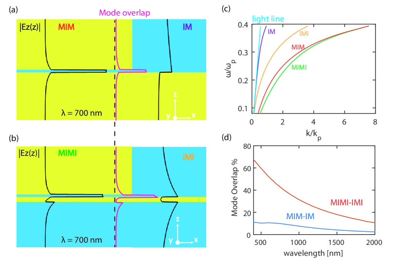
To begin with, we show why optically thin metallic substrates can facilitate high-Purcell and high radiative-efficiency plasmonics via a mode-overlap analysis. Film-coupled nanoparticles can be understood as Fabry-Perot cavities 59, 60, 61 of gap plasmons, with two radiative channels: one into propagating surface plasmon polaritons (SPPs), and another into photons via adiabatic tapering effect 62, 54, 63 using nanoparticle edges. Fig. 3(a) shows the conventionally used metal-insulator-metal (MIM) SPP for emission enhancement. If we reduce the thickness of metal substrate so that it is smaller than the skin depth of MIM SPP, the lower dielectric half space starts to have a decaying tail. We call this new type of SPP the metal-insulator-metal-insulator (MIMI) SPP [Fig. 3(b)]. Surprisingly, although we use less metal, the MIMI SPP achieves better light confinement (smaller ) than the MIM SPP given the same frequency, as shown in the dispersion diagram [Fig. 3(c)]. This indicates that the on-resonance local density of states of the MIMI SPP will be higher than that of the MIM SPP, if one replaces the top metal layer with a nanoparticle as a frequency-selecting cavity. A better mode overlap 62, 64 (middle of Fig. 3(a)(b) and see Supplementary Information) between the gap plasmon with the corresponding propagating SPP implies a larger radiative decay rate into propagating SPP than that in the case using an optically thick film. Fig. 3(d) shows that the MIMI-IMI overlap is much larger than the MIM-IM overlap over a wide wavelength range, from near infrared to the entire visible spectrum. Note that although the above analysis only discusses the mode matching between gap and propagating SPPs, the photon decay rate can be greatly enhanced via tapering the SPPs into photons using the momenta provided by nanoparticle edges, which we will show later.
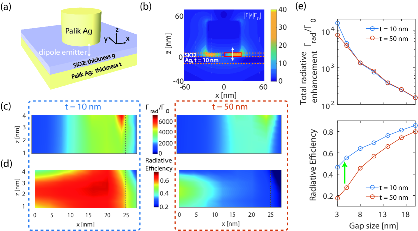
Next, we move from the analytical modal analysis to rigorous computations of the enhanced emission characteristics for realistic structures. We consider a structure with a silver cylinder on top of a silver thin film [Fig. 4(a)]. The permittivities of the cylinder and the film are both Palik silver52 to offer a worst-case scenario analysis. For this structure, the radiative (photon + plasmon) efficiency is calculated to be 60% and 30% for and nm respectively using the scattering and extinction cross-sections of the cylinder, as shown in Fig. S5. As the electric field is dominated by , a z-polarized dipole (marked by the white arrow) is placed within the gap to probe the enhancement [Fig. 4(b)]. A sweeping analysis of dipole location in the plane (marked by the solid red box) provides all the information about the enhancement due to the rotational symmetry of the structure. As shown in Fig. 4(c), the radiative decay rate is generally higher with the thin film ( nm) than that with the thick film ( nm). More surprisingly, in the nm case remains almost uniformly high in the plane with an average of 60%, while that in the case drops to 30% (Fig. 4(d). Both results are consistent with their scattering-extinction ratio (Fig. S5). Note that in the nm case, remains high even for dipole locations within 1-nm distance from the metal surface, where absorption is always considered dominant 30, 31, 26. If epitaxial silver is used for the metal substrate, similar results are obtained with even higher , as shown in Fig. S6. Fig. 4(e) compares and as a function of dielectric gap size for and nm cases, with a fixed emitter at the center of the gap, and under the edge of the cylinder. The trends of are similar. For , in the nm case it remains higher for all gap sizes. The advantage becomes more striking with vanishing gap size (38 nm), where the thin substrate achieves a much higher enhancement and efficiency simultaneously.
The optically thin metallic susbstrates have two main advantages compared to the thick ones. First, the cavity mode becomes less absorptive as shown by the loss per volume (smaller , see Fig. S5). Second, the radiative decay rate is enhanced (larger ) because of the improved mode overlap condition (Fig. 3).
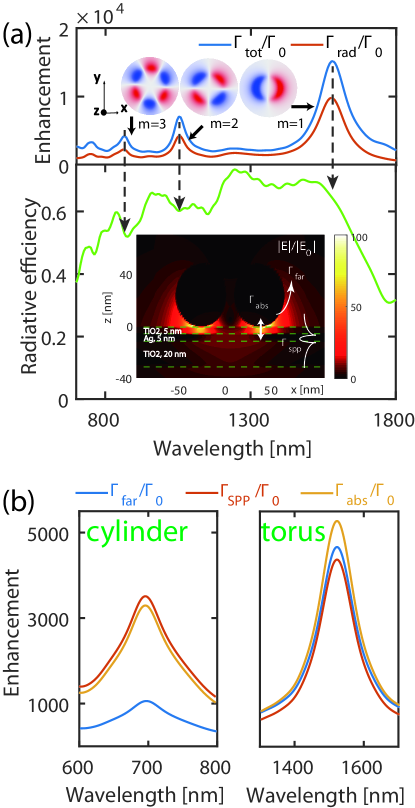
As there are two radiative channels in the gap plasmon structure (i.e., free space radiation into the far field and SPP excitation ), it is important to separate the total radiative decay rate into the two channels (see supporting information) and know how to tailor their relative ratio. It has been shown that tapered antennas (particles like spheres and tori) have higher radiative efficiencies than rigid antennas (particles like cubes and cylinders) 36. Here we show the ratio of and in the entire radiation can be tailored via the shape of nanoparticles. We replace the cylinder with a torus, as shown in Fig. 5. There are multiple orders of gap plasmon resonances (whispering gallery modes with the dielectric gap) in this structure. Usually the decay of high-order resonances of a plasmonic nanoantenna is dominated by absorption and thus are not very efficient for excitation or radiation. However, with a thin metal substrate, the first three gap plasmon resonances of the structure (denoted by their azimuthal index ) all achieve considerably high enhancement, while maintaining high efficiencies [Fig. 5(a)]. This result reveals the potential for high-efficiency harmonic generation and wave multiplexing. For the cylinder, is the dominant radiative channel [Fig. 5(b) left], making this structure an ideal candidate for a high excitation-efficiency plasmon source 41, 42, 43, 44. While for the torus, is greatly boosted, which is useful for fluorescence applications 30, 29, 31 [Fig. 5(b) right]. Note that although the photon and plasmon excitation ratio is different in the two nanoparticles, it is the thin metallic substrate that gives rise to the high total radiative enhancement.
The aforementioned high-Q scattering and high-QY emission are deeply connected via the radiative efficiency but differ from each other. For scattering, . For plasmon-enhanced emission, . Thus, two applications focus on and respectively. What they need in common is a higher for either stronger scattering or higher quantum yield. Another difference is that a high-quality metallic substrate is not essential for high-efficiency (>50%) emission (compare Fig. 4(c)(d) with Fig. S6), as the improved mode matching does not rely on low-absoprtion materials. Nevertheless, it is necessary if one intends to exceed the of the nanoparticle material by using the thin metallic substrate (see Fig. 2).
It is also important to consider the practical feasibility of fabricating such high-quality thin films, and whether the material can be approximated with a local (bulk) permittivity. Theoretically, nonlocal effects 65 induce additional loss when the dimension of plasmonic structures becomes small. Specifically for multifilms, the nonlocal effects are typically insignificant with geometrical sizes larger than 12 nm 66 (or 67, is the plasma wavelength) in the gap plasmon resonances. In addition, the nanoparticles discussed in this Letter are generally large enough (size > 20 nm) such that the nonlocal effects are negligible, yet small enough (size < /10) such that the quasistatic approximation still holds. Overall, the local response approximation is still valid in the above analysis. Practically, the low-temperature epitaxial growth technique can provide a low growth rate (typically 1 angstrom/minute 8) while maintaining high film quality, making this technique ideal for the fabrication of low-loss ultrathin film ( 10 nm).
In this letter, we show that optically thin metallic films offer an ideal platform for high-radiative-efficiency plasmonics. Using a thin metallic substrate, we achieve high- and strong scattering that exceeds the quasistatic limit of the nanoparticle material. Based on the improved mode matching condition, we predicted large-Purcell () and high-efficiency (>50%) for gap-plasmon-enhanced spontaneous emission, maintained over the whole active region. Future efforts can be made on particle designs that enable accurate and high dynamic-range control of the plasmon and photon excitation. It will also be interesting to study how resonances interfere 68, 69, 56 with each other on this platform.
The authors thank Prof. Koppens for the suggestion to look into epitaxially grown silver. The authors thank Di Zhu, Adi Pick, Dr. Homer Reid, Dr. Jianji Yang for helpful discussions. Y. Y. was partly supported by the MRSEC Program of the National Science Foundation under Grant No. DMR-1419807. B. Z. and M. S. were partly supported by S3TEC, an Energy Frontier Research Center funded by the US Department of Energy under grant no. DE-SC0001299. B. Z. was partially supported by the United States-Israel Binational Science Foundation (BSF) under award no. 2013508. C. W. H. was partly supported by the National Science Foundation through grant no. DMR-1307632. O. D. M. was supported by the Army Research Office through the Institute for Soldier Nanotechnologies under contract no. W911NF-13-D-0001.
Numerical methods (Supplementary Texts); Analytical mode overlap calculation (Supplementary Texts); Evolution of Mie and gap plasmon resonances when the torus is moving toward the multifilm (Fig. S1); Multifilm transmission (Fig. S2); Mode squeezing (Fig. S3); Energy concentration coefficients as functions of the silver film thickness (Fig. S4); Radiation efficiencies of the silver cylinder and corresponding absorption per volume for thin and thick silver substrates (Fig. S5); Spontaneous emission enhancement using epitaxial-grown silver substrates (Fig.S6).
References
- Khurgin 2015 Khurgin, J. B. Nat. Nanotechnol. 2015, 10, 2–6
- Sobhani et al. 2015 Sobhani, A.; Manjavacas, A.; Cao, Y.; McClain, M. J.; García de Abajo, F. J.; Nordlander, P.; Halas, N. J. Nano Lett. 2015, 15, 6946–6951
- Liu et al. 2012 Liu, W.; Miroshnichenko, A. E.; Neshev, D. N.; Kivshar, Y. S. ACS Nano 2012, 6, 5489–5497
- Chang et al. 2011 Chang, W.-S.; Willingham, B. A.; Slaughter, L. S.; Khanal, B. P.; Vigderman, L.; Zubarev, E. R.; Link, S. Proc. Natl. Acad. Sci. 2011, 108, 19879–19884
- Peer et al. 2007 Peer, D.; Karp, J. M.; Hong, S.; Farokhzad, O. C.; Margalit, R.; Langer, R. Nat. Nanotechnol. 2007, 2, 751–760
- Ota et al. 2013 Ota, S.; Wang, S.; Wang, Y.; Yin, X.; Zhang, X. Nano Lett. 2013, 13, 2766–2770
- Maier et al. 2003 Maier, S. A.; Kik, P. G.; Atwater, H. A.; Meltzer, S.; Harel, E.; Koel, B. E.; Requicha, A. A. Nat. Mater. 2003, 2, 229–232
- Wu et al. 2014 Wu, Y.; Zhang, C.; Estakhri, N. M.; Zhao, Y.; Kim, J.; Zhang, M.; Liu, X.-X.; Pribil, G. K.; Alù, A.; Shih, C.-K.; Li, X. Adv. Mater. 2014, 26, 6106–6110
- McPeak et al. 2015 McPeak, K. M.; Jayanti, S. V.; Kress, S. J.; Meyer, S.; Iotti, S.; Rossinelli, A.; Norris, D. J. ACS Photonics 2015, 2, 326–333
- Babar and Weaver 2015 Babar, S.; Weaver, J. Appl. Opt. 2015, 54, 477–481
- Miller et al. 2014 Miller, O. D.; Johnson, S. G.; Rodriguez, A. W. Phys. Rev. Lett. 2014, 112, 157402
- Koenderink 2010 Koenderink, A. F. Opt. Lett. 2010, 35, 4208–4210
- Sauvan et al. 2013 Sauvan, C.; Hugonin, J.-P.; Maksymov, I.; Lalanne, P. Phys. Rev. Lett. 2013, 110, 237401
- Kristensen and Hughes 2013 Kristensen, P. T.; Hughes, S. ACS Photonics 2013, 1, 2–10
- Lee and El-Sayed 2005 Lee, K.-S.; El-Sayed, M. A. J. Phys. Chem. B 2005, 109, 20331–20338
- El-Sayed et al. 2005 El-Sayed, I. H.; Huang, X.; El-Sayed, M. A. Nano Lett. 2005, 5, 829–834
- Anker et al. 2008 Anker, J. N.; Hall, W. P.; Lyandres, O.; Shah, N. C.; Zhao, J.; Van Duyne, R. P. Nat. Mater. 2008, 7, 442–453
- Saha et al. 2012 Saha, K.; Agasti, S. S.; Kim, C.; Li, X.; Rotello, V. M. Chem. Rev. 2012, 112, 2739–2779
- Hsu et al. 2014 Hsu, C. W.; Zhen, B.; Qiu, W.; Shapira, O.; DeLacy, B. G.; Joannopoulos, J. D.; Soljačić, M. Nat. Commun. 2014, 5, 3152
- Hsu et al. 2015 Hsu, C. W.; Miller, O. D.; Johnson, S. G.; Soljačić, M. Opt. Express 2015, 23, 9516–9526
- Saito and Tatsuma 2015 Saito, K.; Tatsuma, T. Nanoscale 2015, 7, 20365–20368
- Wang and Shen 2006 Wang, F.; Shen, Y. R. Phys. Rev. Lett. 2006, 97, 206806
- Raman et al. 2013 Raman, A.; Shin, W.; Fan, S. Phys. Rev. Lett. 2013, 110, 183901
- Miller et al. 2014 Miller, O. D.; Hsu, C. W.; Reid, M. T. H.; Qiu, W.; DeLacy, B. G.; Joannopoulos, J. D.; Soljačić, M.; Johnson, S. G. Phys. Rev. Lett. 2014, 112, 123903
- Miller et al. 2016 Miller, O. D.; Polimeridis, A. G.; Reid, M. T. H.; Hsu, C. W.; DeLacy, B. G.; Joannopoulos, J. D.; Soljačić, M.; Johnson, S. G. Opt. Express 2016, 24, 3329–3364
- Anger et al. 2006 Anger, P.; Bharadwaj, P.; Novotny, L. Phys. Rev. Lett. 2006, 96, 113002
- Kühn et al. 2006 Kühn, S.; Håkanson, U.; Rogobete, L.; Sandoghdar, V. Phys. Rev. Lett. 2006, 97, 017402
- Russell et al. 2012 Russell, K. J.; Liu, T.-L.; Cui, S.; Hu, E. L. Nat. Photonics 2012, 6, 459–462
- Rose et al. 2014 Rose, A.; Hoang, T. B.; McGuire, F.; Mock, J. J.; Ciracì, C.; Smith, D. R.; Mikkelsen, M. H. Nano Lett. 2014, 14, 4797–4802
- Akselrod et al. 2014 Akselrod, G. M.; Argyropoulos, C.; Hoang, T. B.; Ciracì, C.; Fang, C.; Huang, J.; Smith, D. R.; Mikkelsen, M. H. Nat. Photonics 2014, 8, 835–840
- Eggleston et al. 2015 Eggleston, M. S.; Messer, K.; Zhang, L.; Yablonovitch, E.; Wu, M. C. Proc. Natl. Acad. Sci. 2015, 112, 1704–1709
- Pelton 2015 Pelton, M. Nat. Photonics 2015, 9, 427–435
- Purcell 1946 Purcell, E. M. Phys. Rev. 1946, 69, 681
- Vesseur et al. 2010 Vesseur, E. J. R.; de Abajo, F. J. G.; Polman, A. Phys. Rev. B 2010, 82, 165419
- Bohren and Huffman 2008 Bohren, C. F.; Huffman, D. R. Absorption and scattering of light by small particles; John Wiley & Sons, 2008
- Faggiani et al. 2015 Faggiani, R.; Yang, J.; Lalanne, P. ACS Photonics 2015, 2, 1739–1744
- Novotny and Hecht 2012 Novotny, L.; Hecht, B. Principles of nano-optics; Cambridge university press, 2012
- Esteban et al. 2010 Esteban, R.; Teperik, T.; Greffet, J.-J. Phys. Rev. Lett. 2010, 104, 026802
- Moreau et al. 2012 Moreau, A.; Ciracì, C.; Mock, J. J.; Hill, R. T.; Wang, Q.; Wiley, B. J.; Chilkoti, A.; Smith, D. R. Nature 2012, 492, 86–89
- Belacel et al. 2013 Belacel, C.; Habert, B.; Bigourdan, F.; Marquier, F.; Hugonin, J.-P.; de Vasconcellos, S. M.; Lafosse, X.; Coolen, L.; Schwob, C.; Javaux, C.; Dubertret, B.; Greffet, J.-J.; Senellart, P.; Maitre, A. Nano Lett. 2013, 13, 1516–1521
- Koenderink 2009 Koenderink, A. F. Nano Lett. 2009, 9, 4228–4233
- Gonzalez-Tudela et al. 2011 Gonzalez-Tudela, A.; Martin-Cano, D.; Moreno, E.; Martin-Moreno, L.; Tejedor, C.; Garcia-Vidal, F. J. Phys. Rev. Lett. 2011, 106, 020501
- Gan et al. 2012 Gan, C. H.; Hugonin, J.-P.; Lalanne, P. Phys. Rev. X 2012, 2, 021008
- Kumar et al. 2014 Kumar, S.; Kristiansen, N. I.; Huck, A.; Andersen, U. L. Nano Lett. 2014, 14, 663–669
- Newton 2013 Newton, R. G. Scattering theory of waves and particles; Springer Science & Business Media, 2013
- Hamam et al. 2007 Hamam, R. E.; Karalis, A.; Joannopoulos, J. D.; Soljačić, M. Phys. Rev. A 2007, 75, 053801
- Ruan and Fan 2012 Ruan, Z.; Fan, S. Phys. Rev. A 2012, 85, 043828
- Mary et al. 2005 Mary, A.; Dereux, A.; Ferrell, T. L. Phys. Rev. B 2005, 72, 155426
- Dutta et al. 2008 Dutta, C. M.; Ali, T. A.; Brandl, D. W.; Park, T.-H.; Nordlander, P. J. Chem. Phys. 2008, 129, 084706
- Teperik and Degiron 2011 Teperik, T.; Degiron, A. Phys. Rev. B 2011, 83, 245408
- Rakovich et al. 2015 Rakovich, A.; Albella, P.; Maier, S. A. ACS Nano 2015, 9, 2648–2658
- Palik 1998 Palik, E. D. Handbook of optical constants of solids; Academic press, 1998; Vol. 3
- Kim 1996 Kim, S. Appl. Opt. 1996, 35, 6703–6707
- Yamamoto et al. 2010 Yamamoto, N.; Ohtani, S.; Garcia de Abajo, F. J. Nano Lett. 2010, 11, 91–95
- Ruppin 2002 Ruppin, R. Phys. Lett. A 2002, 299, 309–312
- Hsu et al. 2014 Hsu, C. W.; DeLacy, B. G.; Johnson, S. G.; Joannopoulos, J. D.; Soljačić, M. Nano letters 2014, 14, 2783–2788
- Pors and Bozhevolnyi 2015 Pors, A.; Bozhevolnyi, S. I. ACS Photonics 2015, 2, 228–236
- Lian et al. 2015 Lian, H.; Gu, Y.; Ren, J.; Zhang, F.; Wang, L.; Gong, Q. Phys. Rev. Lett. 2015, 114, 193002
- Bozhevolnyi and Søndergaard 2007 Bozhevolnyi, S. I.; Søndergaard, T. Opt. Express 2007, 15, 10869–10877
- Miyazaki and Kurokawa 2006 Miyazaki, H. T.; Kurokawa, Y. Phys. Rev. Lett. 2006, 96, 097401
- Yang et al. 2012 Yang, J.; Sauvan, C.; Jouanin, A.; Collin, S.; Pelouard, J.-L.; Lalanne, P. Opt. Express 2012, 20, 16880–16891
- Johnson et al. 2002 Johnson, S. G.; Bienstman, P.; Skorobogatiy, M.; Ibanescu, M.; Lidorikis, E.; Joannopoulos, J. Phys. Rev. E 2002, 66, 066608
- Fernández-Domínguez et al. 2010 Fernández-Domínguez, A.; Maier, S.; Pendry, J. Phys. Rev. Lett. 2010, 105, 266807
- Palamaru and Lalanne 2001 Palamaru, M.; Lalanne, P. Appl. Phys. Lett. 2001, 78, 1466–1468
- Mortensen et al. 2014 Mortensen, N. A.; Raza, S.; Wubs, M.; Søndergaard, T.; Bozhevolnyi, S. I. Nature Commun. 2014, 5
- Ciracì et al. 2012 Ciracì, C.; Hill, R.; Mock, J.; Urzhumov, Y.; Fernández-Domínguez, A.; Maier, S.; Pendry, J.; Chilkoti, A.; Smith, D. Science 2012, 337, 1072–1074
- Yan et al. 2012 Yan, W.; Wubs, M.; Mortensen, N. A. Effects of nonlocal response on the density of states of hyperbolic metamaterials. SPIE NanoScience+ Engineering. 2012; pp 84550V–84550V
- Wang et al. 2006 Wang, H.; Wu, Y.; Lassiter, B.; Nehl, C. L.; Hafner, J. H.; Nordlander, P.; Halas, N. J. Proc. Natl. Acad. Sci. 2006, 103, 10856–10860
- Mukherjee et al. 2010 Mukherjee, S.; Sobhani, H.; Lassiter, J. B.; Bardhan, R.; Nordlander, P.; Halas, N. J. Nano Lett. 2010, 10, 2694–2701