Polarization and Valley Switching in Monolayer Group-IV Monochalcogenides
Abstract
Group-IV monochalcogenides are a family of two-dimensional puckered materials with an orthorhombic structure that is comprised of polar layers. In this article, we use first principles calculations to show the multistability of monolayer SnS and GeSe, two prototype materials where the direction of the puckering can be switched by application of tensile stress or electric field. Furthermore, the two inequivalent valleys in momentum space, which dictated by the puckering orientation, can be excited selectively using linearly polarized light, and this provides additional tool to identify the polarization direction. Our findings suggest that SnS and GeSe monolayers may have observable ferroelectricity and multistability, with potential applications in information storage.
pacs:
85.50 Gk, 64.70 Nd, 71.20 MgThe discovery of 2D materials that can be isolated into single layers through exfoliation and exhibit novel properties has established new paradigms for ultrathin devices based on atomically sharp interfaces Miro et al. (2014); Nicolosi et al. (2013). In particular, transition metal dichalcogenides (TMDs) have been studied extensively and have shown potential for many technological applications ranging from photovoltaics to valleytronic devices Wang et al. (2012); Johari and Shenoy (2012); Chhowalla et al. (2013); Zeng et al. (2012); Xiao et al. (2012); Sie et al. (2014); Kim et al. (2014). The family of monolayer 2D materials has recently grown to include other 2D semiconductors, such as phosphorene and related materials.
However, one of the features thus far lacking for applications both in 2D electronics and in valleytronics is non-volatile memory. Ferromagnetism, an essential element in spintronic memories, is believed to be achievable in graphene and other 2D materials but so far remains difficult to realize and control Sepioni et al. (2010). Ferroelectric memories, in which the information is stored in the orientation of the electric dipole rather than in the magnetization are a possible option. Single-layer graphene (SLG) ferroelectric field-effect transistors (FFET) with symmetrical bit writing have been demonstrated Song et al. (2011), but the prototypes rely on bulk or thin film ferroelectric substrates Song et al. (2011) or ferroelectric polymers Zheng et al. (2010), rather than on crystalline atomically thin ferroelectric materials. An altogether different approach to information storage relies on phase change materials, where the bit value corresponds to a distinct structural phase of the material. Researchers have recently optimized the phase switching energy by using superlattice structures where the movement of the atoms is confined to only one dimension Simpson et al. (2011).
In this article, we analyze the stability of group-IV monochalcogenide MX (M=Ge or Sn, and X=S or Se) monolayers, paying particular interest to their potential as memory functional materials. As prototypes, we use SnS and GeSe. In ambient conditions, bulk SnS and GeSe crystallize in the orthorhombic structure of the space group. At 878 K, SnS goes through a second-order displacive phase transition into the -SnS phase with symmetry Alptekin (2011); Chattopadhyay et al. (1984), which is also a layered phase that can be viewed as a distorted rocksalt structure. For bulk GeSe, such a phase transition has not been observed. Instead, at 924 K bulk GeSe transforms into the rocksalt phase (). This phase can also be stabilized using external pressure Deringer et al. (2014).
Similar to phosphorene Rodin et al. (2014); Liu et al. (2014), SnS and GeSe can be exfoliated Brent et al. (2015); Mukherjee et al. (2013). In monolayer form, they feature multiple valleys, large spin-orbit splittingGomes and Carvalho (2015) and a piezoelectric coefficient that surpasses that of the TMDs Fei et al. (2015); Gomes et al. (2015). Having an in-plane polar axis makes SnS and GeSe monolayers capable of a mechanical response to an applied electric field.
Here, we use density functional theory (DFT) calculations to characterize the multistability of SnS and GeSe, exploring ways in which the phase transitions and domain switch can be triggered externally. We start by demonstrating how the reversible phase transition can be induced by uniaxial stress or electric field. Then, we show how the phase and lattice orientation states can be detected using the valley properties.
I Methods
The calculations were based on density functional theory (DFT) implemented in the Quantum ESPRESSO package Giannozzi et al. (2009). The generalized gradient approximation (GGA) of Perdew-Burke-Ernzerhof (PBE) was used for the exchange and correlation functional, and Troullier-Martins type pseudopotentials Troullier and Martins (1991). The Kohn-Sham orbitals were expanded in a plane-wave basis with a cutoff energy of 70 Ry, and for the charge density a cutoff of 280 Ry was used. A -point grid sampling grid was generated using the Monkhorst-Pack scheme with 10101 points Monkhorst and Pack (1976), and a finer regular grid of 80801 was used for transition probability calculations. The equilibrium structures were found by using a conjugate-gradient optimization algorithm, and the energy landscape is mapped by relaxing the structure under constraints for each of the in-plane lattice parameters, while all the other structural parameters are allowed to relax.
We used the modern theory of polarization King-Smith and Vanderbilt (1993) to calculate the spontaneous polarization given by
| (1) |
where is the ionic charge plus the core electrons, is the position of ions, is the unit cell volume, is the elementary charge, is the valence band index, is the wave vector, and is the electronic wave function. The first term is the contribution from ions and core electrons, and the second term is the electronic contribution defined as adiabatic flow of current which can be calculated from the Berry connection King-Smith and Vanderbilt (1993).The response of the material to a homogenous static external electric field is calculated based on methods developed by Refs. Souza et al. (2002); Umari and Pasquarello (2002) implemented in the Quantum ESPRESSO package Giannozzi et al. (2009).

II Results
II.1 Multistability of SnS and GeSe in the monolayer phase
We start by exploring the energy landscape of monolayer SnS and GeSe. We consider the monolayer form of the two structures that are known for bulk SnS ie., a centrosymmetric structure (), and the structure resembling black phosphorus, and which is the only known layered structure of bulk GeSe. We will designate the respective monolayer phases by appending ‘ML’ to the respective bulk space group.
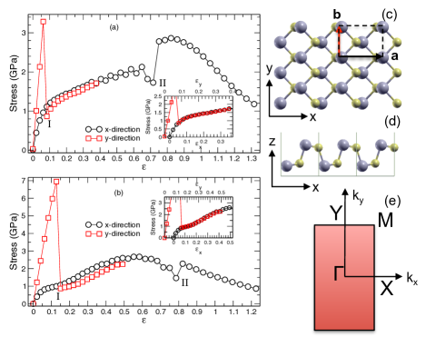
The atomic positions in the -ML phase are (M:0.25, 0.25, 0.05; X:0.25, 0.25, -0.05) in fractional coordinates, where M=(Sn, Ge) and X=(S, Se), and 0.08 for SnS and GeSe, respectively. The -ML phase is obtained by taking . As a result, the -ML has two perpendicular mirror symmetry planes, as well as inversion symmetry, while -ML has no inversion symmetry. In our DFT simulations we used as a tolerance to distinguish the -ML phase from the -ML phase 333We define puckering orientation as a unit vector of the in plane bond formed by the nearest neighbor of MX atoms in the direction of the broken mirror symmetry. For the SnS structure shown in Fig. 2(d), the puckering direction as we define ..
The -ML and the -ML phases can both be seen as distortions of a rocksalt bilayer that can be transformed into each other by a displacement of some of the atoms along (see Fig.2 for and directions). The -ML and -ML phases of SnS and GeSe monolayer have also been reported in Ref. Mehboudi et al. (2016). By symmetry, there are four distinct -ML configurations (equivalent by rotations of the puckering direction). For SnS, -ML is a local minima of the energy surface. For GeSe, the -ML structure is not an energy minimum but a saddle point. The activation energy for reorientation of the -ML puckering direction is very small (88 meV for SnS and 43 meV for GeSe). We note that GGA has been successful in predicting the small enthalpy differences (tens of meV) between different phases of ferroelectric materials, because systematic errors cancel out when comparing systems with very similar structures Sanna et al. (2011). The broken inversion symmetry and total energy with a typical double-well potential of SnS and GeSe are the first two indications that these materials may possess ferroelectricity.
II.2 Application of uniaxial stress
The phase transition of SnS to -ML, or equivalently the reorientation of the -ML structure, can be induced by in-plane uniaxial tensile stress (Fig. 2). We use an effective thickness to estimate the values of stress, as outlined in Ref. Gomes et al. (2015).
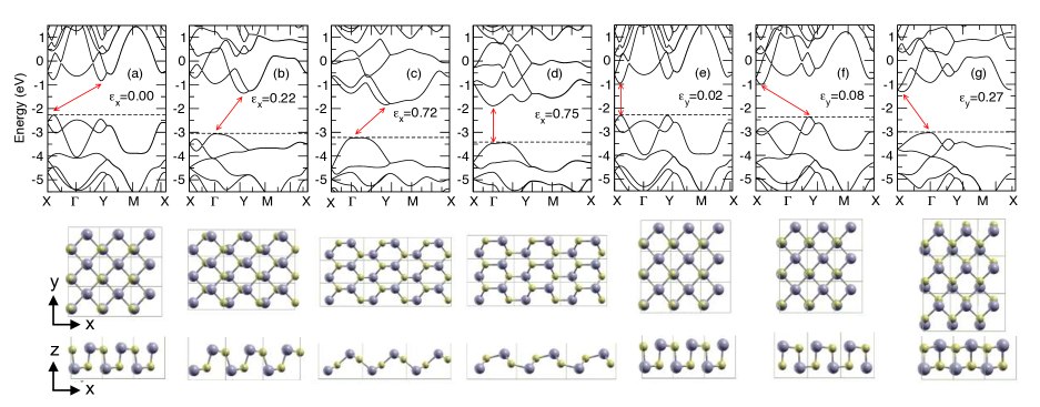
For uniaxial stress along , the SnS structure begins to resemble -ML as the shorter lattice parameter is stretched. For , uniaxial stress results in the rotation of the -ML structure by . The puckering thus rotates from to [Fig. 2(a), transition I]. Similar qualitative behavior is observed in GeSe (see Fig. 2(b)). Both SnS and GeSe transit to phase, but they spontaneously revert back to once the tensile stress is removed 444 We found that once the stretch is removed the structure spontaneously reverts back to for both SnS and GeSe. However, we found that during compression, the phase of SnS is stable..
The application of uniaxial stress along reveals another phase transition at and 0.78 for SnS and GeSe, respectively. The structure is a hexagonal phase resembling blue phosphorene (see Ref. Mehboudi et al. (2015)). The hexagonal structure and its band structure are plotted in Fig. 4.
II.3 Application of electric field
Application of an electric field is an alternative way to trigger the transition between different minima on the energy surface of SnS or GeSe. Since the -ML structure is piezoelectric, the application of an electric field along the polar () direction in a mechanically free sample induces strain as well Gomes et al. (2015). However, here we will consider, for simplicity, the application of an electric field to a mechanically clamped sample.
The spontaneous polarization in the -ML phase, which was measured with respect to the centrosymmetric structure by taking as the effective volume the equivalent volume occupied by a layer of the bulk unit cell, is 0.6 and 1.7 C/m2 for SnS and GeSe, respectively, which is comparable to that of 3D ferroelectrics Zhong et al. (1994).
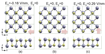
In this case, application of an electric field with polarity opposed to the bond dipole results in bonds breaking and creates new bonds with inversion of the polarization along , rather than in a rotation of the structure. As shown in Fig. 3 (a) the ionic configuration changes (i.e., switches from to ), and it is apparent from Eq. 1 that the electric dipole orientation can be switched, which we have found to be the case based on our DFT calculations.
The coercive field for this puckering transformation is 0.18 V/cm for SnS and 0.51 V/cm for GeSe. Moreover, we found that applying an electric field in at 0.29 V/cm (0.80 V/cm) could also convert the from to for SnS (GeSe). The coercive field calculated by this method corresponds to the electric field at which the unfavorable phase becomes unstable and can be seen as an upper bound for the coercive field of a real multi-domain material. This is usually smaller provided that the domain walls are mobile at that temperature and, according to a recent work Wang and Qian (2015), the domain wall energy is small for this class of materials. Thus, the electrical fields necessary for ferroelectric switching are clearly achievable in current 2D experiments Radisavljevic et al. (2011). The structures of SnS monolayer under electric fields at which the puckering orientation switches are plotted in Fig. 3.
Since the two materials possess a spontaneous, reversible polarization and bistability, they classify as ferroelectrics. The configuration-coordinate diagram of GeSe is typical of a ferroelectric with second-order phase transition at (consistent with the change in symmetry). The energy curve for SnS has a minimum rather than a saddle point at -ML, and therefore resembles a ferroelectric with first order phase transition, with the peculiarity that the -ML structure is stable for all . Recently, based on Car-Parrinello molecular dynamics simulations, Mehboudi et al. showed that monolayer monochalcogenides undergo an order-disorder phase transition Mehboudi et al. (2016). Hence, since SnS and GeSe have four degenerate -ML phases, we expect that the average total polarization goes to zero as temperature approaches .
II.4 Band structure
The phase transitions are accompanied by changes of the band structure and can, therefore, be detected optically. Representative SnS and GeSe band structures under uniaxial stress are shown in Fig. 4 and Fig. 5, respectively. We note that even though the band gap is underestimated due to our usage of DFT as the calculation method Gomes and Carvalho (2015), the dispersion of the bands is accurately reproduced. Unstrained SnS is an indirect-gap semiconductor with its valence band maximum located near the X-point (along the -X line) and the conduction band minimum near the Y-point (along the -Y line). There are, therefore, two two-fold degenerate valleys, designated and , respectively. At large strains along , SnS transforms to a hexagonal phase at resembling blue phosphorene (Fig. 4 (c)) Mehboudi et al. (2015) and becomes a direct gap at . For uniaxial stress along there is a transition from indirect gap to direct gap at (see Fig. 4(e)), after which the system again becomes indirect gap.
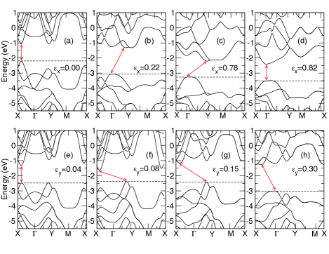
The band structure of GeSe under uniaxial stress is shown in Fig. 5 (a) to (d) for the and (e) to (h) for the . Even though unstrained GeSe is a direct-gap semiconductor, there are also two nearly degenerate conduction band minima at the and points. The swapping between the and of the -ML structure under tensile stress along the direction occurs at and is in this case accompanied by a loss of the direct bandgap, which becomes indirect as the structure reverts back into -ML. As shown in Fig. 5, the band structure (b) is equivalent to the band structure (h) if the and are inverted (rotation around axis on figures). The transition to a hexagonal phase under tensile stress along () is also accompanied by an indirect- to direct-gap semiconductor transition.
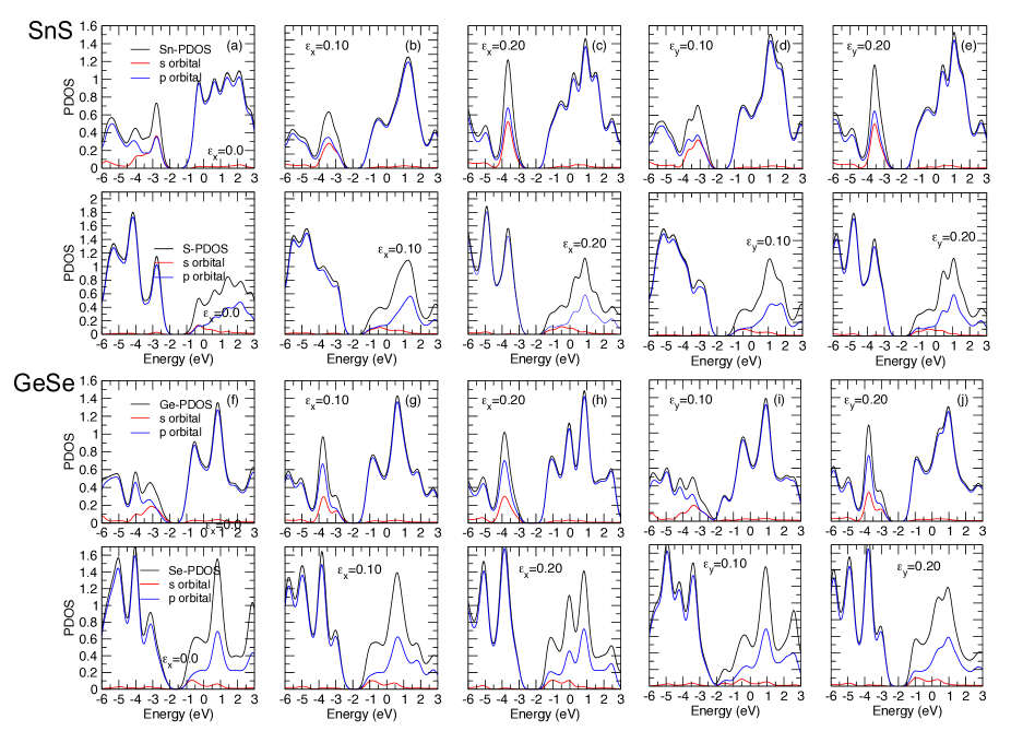
In addition, we calculated the projected density of states for SnS and GeSe for various strains (Fig. 6). The trends of the evolution of PDOS of GeSe and SnS with increasing strain are similar. Specifically, the relative contributions of the -orbitals for Sn and Ge atoms at energies close to the maximum valence band increases with increasing strain.
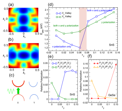
The selection of valleys or can be achieved by at least two different optical methods: (i) using the fact that the direct gap is different at the two valley pairs; or (ii) using the optical selection rules. The direct transitions at the and valleys have different energies, provided there is a means to identify the orientation of the crystal (Fig. 7). We plot the energy difference between valence and conduction band of SnS as functions of in plane wave vectors shown in Fig. 7 (a) and (b). It can be seen that the gap surface of (Fig. 7 (a)) is equivalent to (Fig. 7 (b)) but rotated 90∘. It is evident that under uniaxial stress in the bands have rotated in the Brillouin Zone, i.e. the valley effectively becomes the valley after passing the transition point of =0.08.
II.5 Transition probabilities
Using linearly polarized light to select the valleys or provides an additional method to detect the phase transition optically. The interband transition probability at a given wave vector is given by Rodin et al. (2016); Xiao et al. (2012)
| (2) |
where is the direction of the light polarization, is the conduction band wave function, is the valence band wave function, and is the Hamiltonian. Alternatively, one can relate the transition probability to the dipole moment between the initial and the final bands: , where the momentum direction corresponds to the light polarization. For the transition to be allowed, the dipole moment must not vanish. It is possible to determine whether it is finite or not using the symmetry of the bands and the momentum. Since the dipole moment is computed by integrating the product of the initial and final wave functions, and the momentum, it is nonzero only if this product () is not odd with respect to any of the axes. In other words, the integrand must remain unchanged under every symmetry transformation of the space group characterizing the crystal.
We used our ab initio results to calculate the transition probabilities. For unstrained SnS, -polarized light populates only the valleys, as there is no coupling between the valence and conduction band at in the direction (see Fig. 7 (e)). As shown by Ref. Rodin et al. (2016), the conduction band, valence band, and the have a same irreducible representation. Consequently, the direct product of these quantities results in a non-vanishing transition probability coupling. On the other hand, -polarized light cannot excite , as it possesses different representation. -polarized light can populate both and but it populates predominantly the valleys, with . Similar behavior is observed in GeSe with a smaller selective valley polarization ratio. For instance, with linearly -polarized light the selective valley polarization ratio was found to be . The schematic valley polarization is shown in Fig. 7 (c).
The evolution of local gap and of SnS under stress in the direction is shown in Fig. 7(d). We see that there is an abrupt change in gap near the transition point . We also plot the relative polarization and as a function of axial strain , shown in Fig. 7(e) and (f) for SnS and GeSe, respectively. As we discussed earlier, -polarized light populates predominantly the valleys but there is still a small transition probability at when -polarized light is used. The absorption threshold for -polarized light has an abrupt change near ( for GeSe), when the phase transition takes place. However, the absorption edge for -polarized light changes smoothly.
Before the transition point, the structure has a mirror symmetry inverting , and the valleys can be populated using polarized light along and (the latter with a very small coupling). However, after the transition point, the puckering direction is rotated to be in the , and the reflection symmetry in is broken, whereas a reflection symmetry emerges in . As a result, can be excited by both and polarized light after the transition takes place. We have therefore demonstrated how optical transitions can be used to detect the orientation of the structure which determines valley configurations.
In summary, we have used first-principles calculations to demonstrate the potential of group-IV monochalcogenide monolayers as functional materials for information storage. This strategy, demonstrated using SnS and GeSe as prototypes, relies on the metastability and the possibility of switching the polarization direction using stress or electric field, creating a binary memory device. Comparing these prototype materials, SnS differs from GeSe because it has a stable centrosymmetric phase which, at , is close in energy to the -ML phase.
Due to their peculiar band structures, both SnS and GeSe could in principle be used as functional materials for memory devices that can easily be interfaced with valleytronics logic. Valleytronics is based on the concept that the valley index can potentially be used to store information for subsequent logic operations, equivalent to spin in spintronics. However, in most valleytronics materials the information can be considered non-volatile only up to the timescale defined by inter-valley scattering processes, which are ubiquitous in real materials. Structural changes, used to store information in phase change memory devices, take place on a timescale orders of magnitude longer. Materials such as SnS and GeSe can be used to convert information stored as structural phase into information stored as valley index. One possibility is for example by using near-bandgap light that excites only the pair of valleys corresponding to the lowest energy exciton. The subsequent electronic state will have electron-hole pairs with momentum or , depending on the structure orientation. This valley state can be transmitted onto a valley-filter Gunlycke and White (2011). Alternatively, if coupled to a polarized light detector, the polarization switching can be detected optically taking advantage of valley-dependent direction of the linear polarization of the luminescence Rodin et al. (2016).
Acknowledgements.
P.Z.H. is grateful for the support of the Physics and Mechanical Engineering Departments at Boston University, the hospitality of the NUS Centre for Advanced 2D Materials and Graphene Research Centre where this work was initiated, the support of the Materials Science and Engineering Innovation Grant and the Boston University High Performance Shared Computing Cluster. A.C. acknowledges support by the National Research Foundation, Prime Minister Office, Singapore, under its Medium Sized Centre Programme and CRP award “Novel 2D materials with tailored properties: beyond graphene” (Grant No. R-144-000-295-281). D.K.C. is grateful for the hospitality of the Aspen Center for Physics which is supported by NSF Grant PHY-1066293, and of the International Institute for Physics of the Federal University of Rio Grande do Norte, in Natal, Brazil, where some of this work was completed. HSP acknowledges the support of the Mechanical Engineering Department at Boston University. We thank Alex Rodin for helpful comments and discussions.References
- Miro et al. (2014) P. Miro, M. Audiffred, and T. Heine, Chem. Soc. Rev. 43, 6537 (2014).
- Nicolosi et al. (2013) V. Nicolosi, M. Chhowalla, M. G. Kanatzidis, M. S. Strano, and J. N. Coleman, Science 340 (2013).
- Wang et al. (2012) Q. H. Wang, K. Kalantar-Zadeh, A. Kis, J. N. Coleman, and M. S. Strano, Nature Nanotechnology 7, 699 (2012).
- Johari and Shenoy (2012) P. Johari and V. B. Shenoy, ACS Nano 6, 5449 (2012).
- Chhowalla et al. (2013) M. Chhowalla, H. S. Shin, G. Eda, L.-J. Li, K. P. Loh, and H. Zhang, Nature Chemistry 5, 263 (2013).
- Zeng et al. (2012) H. Zeng, J. Dai, W. Yao, D. Xiao, and X. Cui, Nature Nanotechnology 7, 490 (2012).
- Xiao et al. (2012) D. Xiao, G.-B. Liu, W. Feng, X. Xu, and W. Yao, Phys. Rev. Lett. 108, 196802 (2012).
- Sie et al. (2014) E. J. Sie, J. W. McIver, Y.-H. Lee, L. Fu, J. Kong, and N. Gedik, Nature Materials 14, 290 (2014).
- Kim et al. (2014) J. Kim, X. Hong, C. Jin, S.-F. Shi, C.-Y. S. Chang, M.-H. Chiu, L.-J. Li, and F. Wang, Science 346, 1205 (2014).
- Sepioni et al. (2010) M. Sepioni, R. R. Nair, S. Rablen, J. Narayanan, F. Tuna, R. Winpenny, A. K. Geim, and I. V. Grigorieva, Phys. Rev. Lett. 105, 207205 (2010).
- Song et al. (2011) E. B. Song, B. Lian, S. M. Kim, S. Lee, T.-K. Chung, M. Wang, C. Zeng, G. Xu, K. Wong, Y. Zhou, et al., Applied Physics Letters 99, 042109 (2011).
- Zheng et al. (2010) Y. Zheng, G.-X. Ni, C.-T. Toh, C.-Y. Tan, K. Yao, and B. Özyilmaz, Phys. Rev. Lett. 105, 166602 (2010).
- Simpson et al. (2011) R. Simpson, P. Fons, A. Kolobov, T. Fukaya, M. Krbal, T. Yagi, and J. Tominaga, Nature Nanotechnology 6, 501 (2011).
- Alptekin (2011) S. Alptekin, Journal of Molecular Modeling 17, 2989 (2011).
- Chattopadhyay et al. (1984) T. Chattopadhyay, A. Werner, H. Von Schnering, and J. Pannetier, Revue de Physique Appliquée 19, 807 (1984).
- Deringer et al. (2014) V. L. Deringer, R. P. Stoffel, and R. Dronskowski, Phys. Rev. B 89, 094303 (2014).
- Rodin et al. (2014) A. S. Rodin, A. Carvalho, and A. H. Castro Neto, Phys. Rev. Lett. 112, 176801 (2014).
- Liu et al. (2014) H. Liu, A. T. Neal, Z. Zhu, Z. Luo, X. Xu, D. Tománek, and P. D. Ye, ACS Nano 8, 4033 (2014).
- Brent et al. (2015) J. R. Brent, D. J. Lewis, T. Lorenz, E. A. Lewis, N. Savjani, S. J. Haigh, G. Seifert, B. Derby, and P. O’Brien, Journal of the American Chemical Society 137, 12689 (2015).
- Mukherjee et al. (2013) B. Mukherjee, Y. Cai, H. R. Tan, Y. P. Feng, E. S. Tok, and C. H. Sow, ACS Applied Materials & Interfaces 5, 9594 (2013).
- Gomes and Carvalho (2015) L. C. Gomes and A. Carvalho, Phys. Rev. B 92, 085406 (2015).
- Fei et al. (2015) R. Fei, W. Li, J. Li, and L. Yang, Applied Physics Letters 107, 173104 (2015).
- Gomes et al. (2015) L. C. Gomes, A. Carvalho, and A. H. Castro Neto, Phys. Rev. B 92, 214103 (2015).
- Giannozzi et al. (2009) P. Giannozzi, S. Baroni, N. Bonini, M. Calandra, R. Car, C. Cavazzoni, D. Ceresoli, G. L. Chiarotti, M. Cococcioni, I. Dabo, A. Dal Corso, S. de Gironcoli, S. Fabris, G. Fratesi, R. Gebauer, U. Gerstmann, C. Gougoussis, A. Kokalj, M. Lazzeri, L. Martin-Samos, N. Marzari, F. Mauri, R. Mazzarello, S. Paolini, A. Pasquarello, L. Paulatto, C. Sbraccia, S. Scandolo, G. Sclauzero, A. P. Seitsonen, A. Smogunov, P. Umari, and R. M. Wentzcovitch, Journal of Physics: Condensed Matter 21, 395502 (19pp) (2009).
- Troullier and Martins (1991) N. Troullier and J. L. Martins, Phys. Rev. B 43, 1993 (1991).
- Monkhorst and Pack (1976) H. J. Monkhorst and J. D. Pack, Phys. Rev. B 13, 5188 (1976).
- King-Smith and Vanderbilt (1993) R. D. King-Smith and D. Vanderbilt, Phys. Rev. B 47, 1651 (1993).
- Souza et al. (2002) I. Souza, J. Íñiguez, and D. Vanderbilt, Phys. Rev. Lett. 89, 117602 (2002).
- Umari and Pasquarello (2002) P. Umari and A. Pasquarello, Phys. Rev. Lett. 89, 157602 (2002).
- Note (1) We define puckering orientation as a unit vector of the in plane bond formed by the nearest neighbor of MX atoms in the direction of the broken mirror symmetry. For the SnS structure shown in Fig. 2(d), the puckering direction as we define .
- Mehboudi et al. (2016) M. Mehboudi, A. M. Dorio, W. Zhu, A. van der Zande, H. O. H. Churchill, A. A. Pacheco-Sanjuan, E. O. Harriss, P. Kumar, and S. Barraza-Lopez, Nano Letters 16, 1704 (2016).
- Sanna et al. (2011) S. Sanna, C. Thierfelder, S. Wippermann, T. P. Sinha, and W. G. Schmidt, Phys. Rev. B 83, 054112 (2011).
- Note (2) We found that once the stretch is removed the structure spontaneously reverts back to for both SnS and GeSe. However, we found that during compression, the phase of SnS is stable.
- Mehboudi et al. (2015) M. Mehboudi, K. Utt, H. Terrones, E. O. Harriss, A. A. Pacheco SanJuan, and S. Barraza-Lopez, Proceedings of the National Academy of Sciences 112, 5888 (2015).
- Zhong et al. (1994) W. Zhong, R. King-Smith, and D. Vanderbilt, Physical review letters 72, 3618 (1994).
- Wang and Qian (2015) H. Wang and X. Qian, arXiv preprint arXiv:1606.04522 (2015).
- Radisavljevic et al. (2011) B. Radisavljevic, A. Radenovic, J. Brivio, V. Giacometti, and A. Kis, Nature nanotechnology 6, 147 (2011).
- Rodin et al. (2016) A. S. Rodin, L. C. Gomes, A. Carvalho, and A. H. Castro Neto, Phys. Rev. B 93, 045431 (2016).
- Gunlycke and White (2011) D. Gunlycke and C. T. White, Phys. Rev. Lett. 106, 136806 (2011).