Thickness and electric field dependent polarizability and dielectric constant in phosphorene
Abstract
Based on extensive first principle calculations, we explore the thickness dependent effective dielectric constant and slab polarizability of few layer black phosphorene. We find that the dielectric constant in ultra-thin phosphorene is thickness dependent and it can be further tuned by applying an out of plane electric field. The decreasing dielectric constant with reducing number of layers of phosphorene, is a direct consequence of the lower permittivity of the surface layers and the increasing surface to volume ratio. We also show that the slab polarizability depends linearly on the number of layers, implying a nearly constant polarizability per phosphorus atom. Our calculation of the thickness and electric field dependent dielectric properties will be useful for designing and interpreting transport experiments in gated phosphorene devices, wherever electrostatic effects such as capacitance, charge screening etc. are important.
I Introduction
Monolayer black phosphorene Liu et al. (2014) has emerged as a promising material for p-type FET (field effect transistor) operation, on account of it’s direct bandgap of magnitude 1.5 eV and reasonably high hole mobility value, theoretically predicted and experimentally measured to be around 10,000 and 1,000 cm2V-1s-1, respectivelyLiu et al. (2014); Li et al. (2014a); Qiao et al. (2014). As a consequence, transistors based on phosphorene exhibit excellent ION/IOFF ratio of , as well as carrier mobility comparable to that of MoS2 (200 – 1,000 cm2V-1s-1)Liu et al. (2014); Li et al. (2014a); Xia et al. (2014). Individual layers of black phosphorus have puckered honeycomb like structure and they are held together by weak van-der Waals forces, facilitating separation of monolayer or few layers by mechanical or liquid exfoliationLiu et al. (2014); Guo et al. (2015); Woomer et al. (2015). Phosphorene is a highly anisotropic material and values of elastic modulus, electron and hole effective mass, calculated along mutually orthogonal zigzag and armchair direction, have a ratio of 3.5, 6.6 and 42.3, respectively Qiao et al. (2014), which is also manifested in experimental observations reporting anisotropic electronic transport and optical propertiesLiu et al. (2014); Wang et al. (2015a); Mao et al. (2015); Çak ır et al. (2015).
It has been shown that the intrinsic bandgap of phosphorene and other layered materials can be modulated by applying external perturbation like strain and electric field Dai and Zeng (2014); Li et al. (2014b); Fei and Yang (2014); Çakır et al. (2014); Wang et al. (2015b); Rastogi et al. (2014); Ghosh et al. (2015); Rastogi et al. (2015); Nahas et al. (2015); Wang et al. (2015c). More interestingly, it has also been predicted that an electric field applied out of the plane of phosphorene can induce a tunable Dirac cone, and additionally induce a normal insulator to topological insulator to metal transition Dolui and Quek (2015); Liu et al. (2015). Such studies vividly demonstrate the tunability of electronic properties of multi-layered phosphorene, on application of an external electric field. Motivated by this, in this article we study the thickness and electric field dependent effective dielectric constant of -layers of phosphorene subjected to an out of plane (transverse) electric field. The dielectric constant and polarizability of a material, in addition to being fundamentally important properties, are also very useful for characterizing the material’s electrostatic properties such as electronic charge screening which determines the strength of Coulomb interaction, capacitance, energy storage capacity, and its transport characteristics Santos and Kaxiras (2013a, b); Tóbik and Dal Corso (2004); Yu et al. (2008); Li et al. (2015a).
In this article we use density functional theory (DFT) based electronic structure calculations, including van-der Waals interactions, to explicitly show that the dielectric constant of phosphorene, perpendicular to the phosphorene plane, depends on the number of layers and the strength of the applied transverse electric field. Using these calculations for a few layers (from two to eight) phosphorene, we obtain the bulk dielectric constant and the surface polarizability of phosphorene atoms, which in turn are used to correctly extrapolate the dielectric constant for any number of layers, at least in the low electric field regime. The article is organized as follows: in section II we report the structural parameters and electronic properties of multi-layer phosphorene, followed by a discussion of the impact of transverse electric field on charge screening in section III, and it’s effect on the slab polarizability and dielectric constant in section IV. Finally we summarize our findings in section V.
II Structural and electronic properties of multi-layer phosphorene
We calculate the structural and electronic properties of multilayered black phosphorene based on DFT calculations, using a plane wave basis set (cutoff energy 100 Ry) and norm conserving Troullier Martins pseudopotential,Troullier and Martins (1991) as implemented in Quantum Espresso.Giannozzi et al. (2009) The electron exchange-correlation is treated within the framework of generalized gradient approximation (GGA), as proposed by Perdrew-Burke-Ernzerhof (PBE).Perdew et al. (1996) The dispersion forces among multiple phosphorene layers are taken into account by using non-local van-der Waals exchange correlation functional optB88-vdW.Klimeš et al. (2010); Dion et al. (2004); Thonhauser et al. (2007); Román-Pérez and Soler (2009); Sabatini et al. (2012) Brillouin Zone integrations are performed using a -point grid of . Further we have used a vacuum region of Å in the direction perpendicular to the phosphorene plane to prevent any interaction among the spurious replica images. All the structures are fully optimized until the forces on each atom are less than 0.01 eV/Å. The effect of transverse electric field is simulated using a sawtooth potential, while taking dipole correction into consideration.Bengtsson (1999)
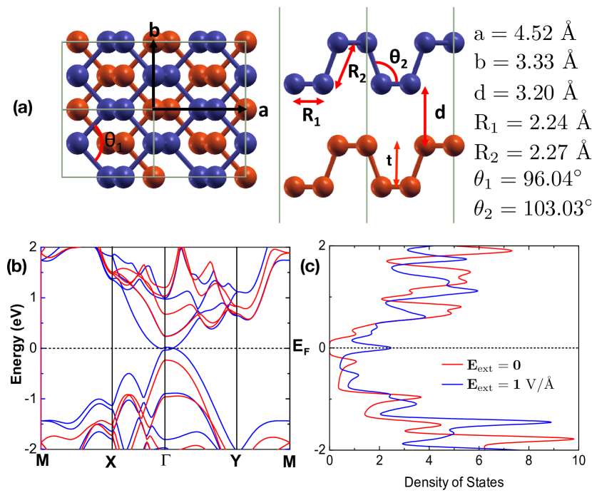
In Fig 1(a), we illustrate the crystal structure and the electronic band structure of AB stacked bilayer phosphorene. Comparing with their bulk values, we find that in bilayer phosphorene the lattice parameter is 0.9% larger, while and inter-layer distance remains the same [see Table 1]. With increasing number of layers, magnitude of decreases towards it’s bulk value of 4.48 Å [see Table 1]. The GGA-PBE estimated bandgap in bilayer phosphorene has a value of 0.48 eV, which decreases towards it’s bulk value of 0.04 eV, the magnitude being inversely proportional to the number of layers [see Table 1]. Although GGA-PBE can qualitatively predict the electronic band structure of a material correctly, it’s limitations are well known regarding bandgap underestimation. For example, a value of 1.04 eV (almost twice than our GGA-PBE estimate) is reported for bilayer phosphorene, based on hybrid functional (HSE06) based calculations, which is known to predict bandgap more accurately.Dai and Zeng (2014) Evidently the band structure is anisotropic (see curvature along -X and -Y directions), which is also going to be reflected in effective mass, mobility etc. and this qualitatively explains the experimentally observed strong directionality of electronic, thermal and optical properties of multilayered black phosphorene.Liu et al. (2014); Wang et al. (2015a); Mao et al. (2015)
| NL | a (Å) | b (Å) | d (Å) | Bandgap (eV) |
|---|---|---|---|---|
| 2 | 4.52 | 3.33 | 3.21 | 0.48 |
| 3 | 4.51 | 3.33 | 3.21 | 0.28 |
| 4 | 4.51 | 3.33 | 3.21 | 0.19 |
| 5 | 4.50 | 3.33 | 3.21 | 0.13 |
| 6 | 4.50 | 3.33 | 3.21 | 0.09 |
| 8 | 4.49 | 3.33 | 3.21 | 0.07 |
| Bulk | 4.48 | 3.33 | 3.21 | 0.04 |
III Impact of a transverse electric field and charge screening
Having described the structural and electronic properties of multi-layered phosphorene, we now proceed to study the impact of a transverse electric field on it. As reported in the literature Dai and Zeng (2014); Dolui and Quek (2015); Liu et al. (2015), with increasing external transverse electric field () in multilayered phosphorene, its bandgap decreases and ultimately reduces to zero [see Fig. 2 (a)], leading to a topological phase transition with a phase characterized by the index Kane and Mele (2005); Roy (2009a, b); Soluyanov and Vanderbilt (2011). However, in this article we will focus on the evolution of the dielectric properties of multi-layered phosphorene in normal insulator state, i.e., before it turns into a topological insulator and eventually into a metal at relatively high transverse electric field.Liu et al. (2015) According to our GGA-PBE calculation, for bilayer phosphorene bandgap closing occurs at V/Å [see Fig. 1(b)-(c)]. The explicit dependence of the bandgap on the transverse electric field is shown in Fig. 2(a). Evidently the critical electric field needed to close the bandgap and induce a topological phase transition decreases with increasing number of layers, which is consistent with the fact that the actual bandgap also varies inversely with number of layers.
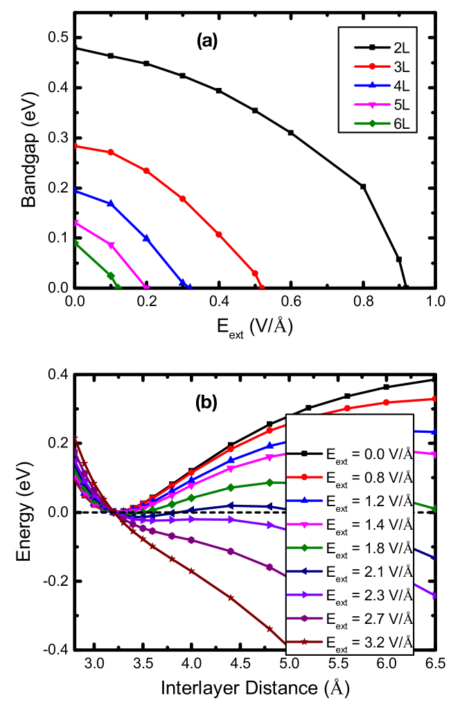
There is a limit to the electric field strength that can be applied to few layers of phosphorene without compromising its structural stability. Binding among adjacent layers [because of van-der Waals (vdW) interaction] are expected to weaken in presence of externally applied electric field, making the structure unstable beyond certain field strength. This is verified by computing the total energy of bilayer phosphorene (measured with reference to it’s energy at equilibrium interlayer spacing of 3.2 Å and zero external field) by changing the interlayer distance, for different values of [see Fig. 2(b)]. The vdW binding energy per phosphorus atom in absence of external electric field is about meV, while that at V/Å, it is meV and it further decreases to zero at V/Å.
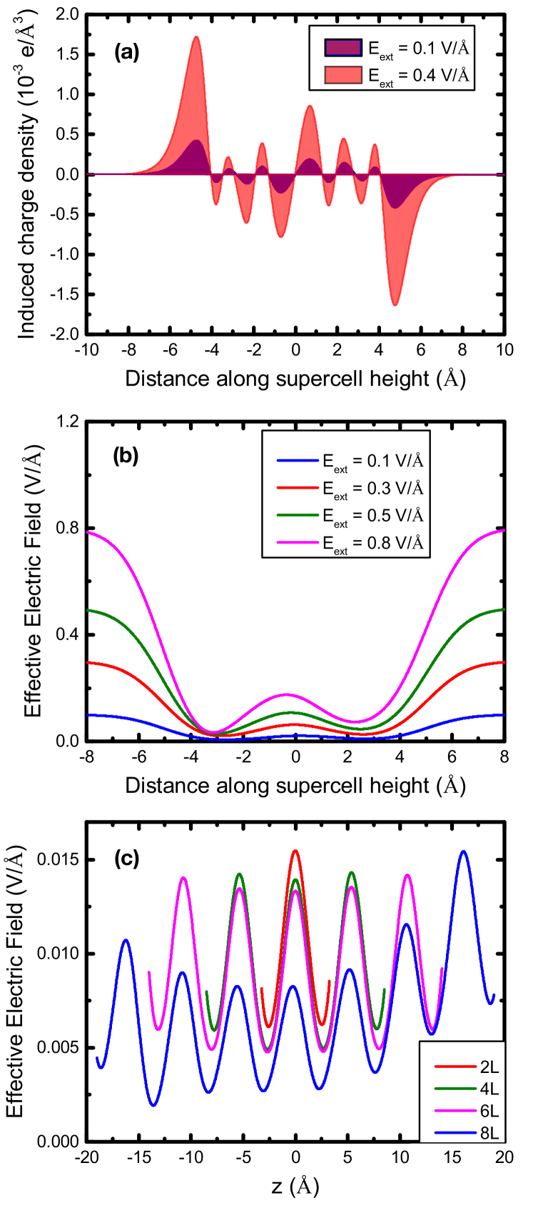
Qualitatively, a vertical electric field pushes the electronic cloud from the bottom surface towards the top surface. This in turn results in induced charge density as depicted in Fig. 3(a), which is qualitatively similar to the induced charge density reported in other 2D materials such as graphene Yu et al. (2008); Santos and Kaxiras (2013a), MoS2 Santos and Kaxiras (2013b), multilayer GaS films Li et al. (2015b) etc. To calculate the effective induced charge density in the direction (perpendicular to the phosphorene layers), denoted by , we take the difference between (charge density in presence of external field) and (charge density in absence of external field), and then average it over the plane of phosphorene layer (x-y plane). In order to smoothen out the variations in the charge density over the inter-atomic distances, we further use a Gaussian (filter) smoothing function, having the width of the order of inter-atomic distance and thus we have
| (1) |
where S denotes the area of the supercell in the x-y plane and the indicates the spatial in-plane average with the Gaussian filter in the direction. This induced ‘macroscopic’ charge density typically increases with increasing electric field.
The induced charge can then be used to calculate the planar averaged and Gaussian filtered effective polarization in the direction using,
| (2) |
along with the boundary condition that the polarization vanishes in the region of vanishing charge density.
The induced charges in turn screens the external electric field by generating a screening electric field (), and consequently the effective electric field inside phosphorene is reduced to . The effective electric field in the direction can be calculated by solving the Poisson equation for the screening potential which arises form the induced charges,
| (3) |
along with the boundary condition that the induced electric field vanishes far away from the region of induced charges.
From an ab-initio perspective, can also be directly calculated by taking the planar average of the difference between Hartree potential (obtained from DFT calculations) at finite electric field and that at zero electric field and differentiating with respect to the vertical distance Santos and Kaxiras (2013a, b): , where . We have checked that the effective electric fields, calculated using both the methods are consistent with each other (within or each other), in the region where there are finite charges, and consequently we will just use Eq. (3) to report the effective electric field used in the rest of the manuscript.
The variation of inside bilayer phosphorene, as function of position along z-axis at different electric field strengths is shown in panel (b) of Fig. 3. Evidently both , as well as the difference of felt by the two layers, increases with increasing applied electric field strength. Aa a consistency check we note that the , at the slab boundaries where the induced charges vanish. In panel (c) of Fig. 3, we study the variation of for different number of layers of phosphorene, as a function of the vertical distance, for a constant V/Å. Note that as the number of layers increase, the effective electric field decreases on account of the increased screening with thickness. We further note that with increasing number of layers, the effective electric field is higher at the surface and decreases gradually inside the material. This is a direct consequence of the fact that at the surface the field is screened only by the charges at the surface but as we move inside the material, the charges on the surface as well as those inside the material screen the external field.
IV Polarizability and the dielectric function
Having discussed the induced charge and the screened effective field, we now focus on the dielectric response of -layer phosphorene. Following Ref. [Giustino and Pasquarello, 2005], the microscopic static permittivity (planer averaged with gaussian filter) can be defined as
| (4) |
Using Eqs. (2)-(4), we can easily show that
| (5) |
which is analogous to the conservation of the displacement field component perpendicular to the interfaces in electrostatics Griffiths (1989). Equation (5) is also the basis for defining the inverse of the permittivity of a slab (of height ) as the average of the inverse of the height dependent permittivity Giustino and Pasquarello (2005)
| (6) |
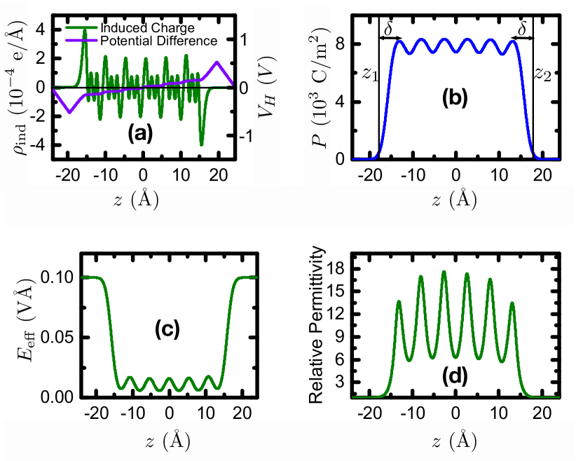
For this manuscript, we consider the slab thickness to be between the points where the polarization drops to of the nearest peak value associated with the topmost or bottommost phosphorene layers, as shown in Fig. 4(b).
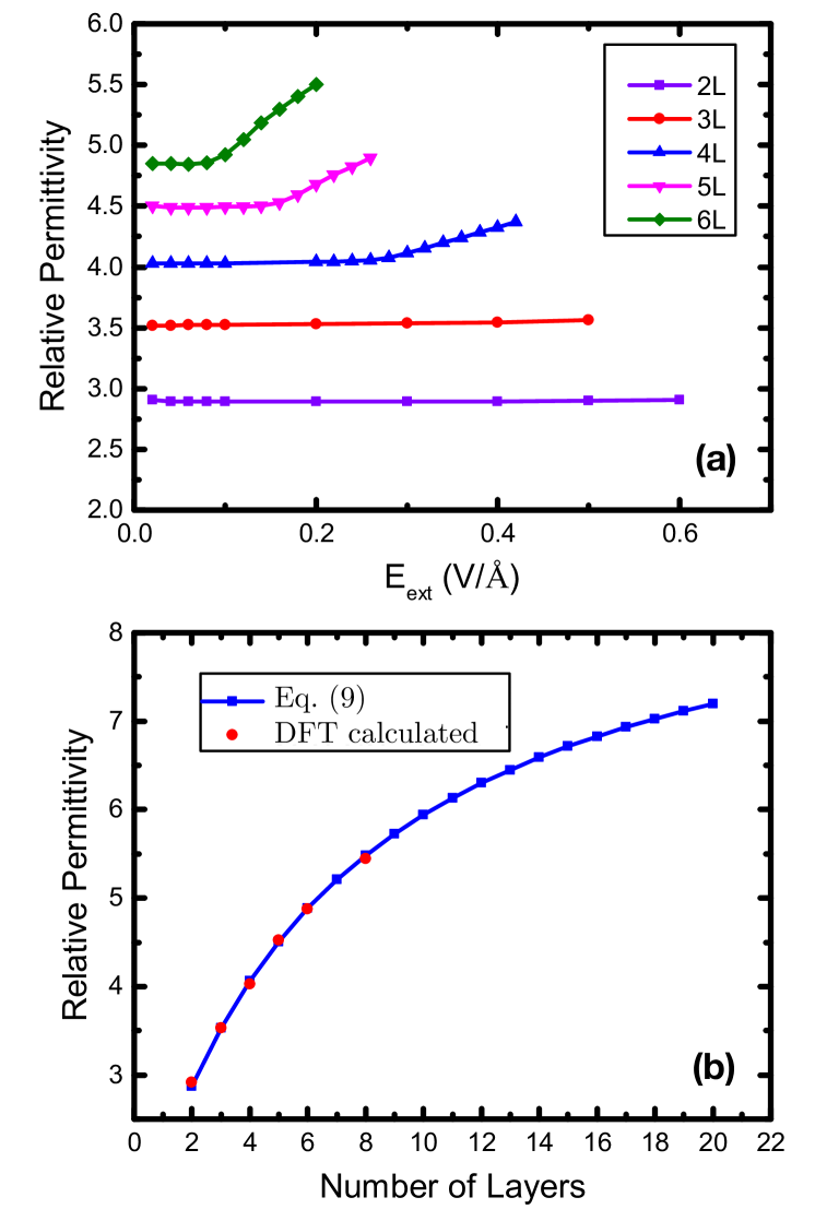
Using the framework described above in Eqs. (1)-(4), we calculate and display the variation of the induced charge and the induced effective potential () as a function of the vertical distance in six layer phosphorene for a fixed external field of V/Å in Fig. 4(a). In panels (b) and (c) of Fig. 4, we study the variation of the (Gaussian filtered) polarization and the effective induced field, respectively, in the vertical direction. Panel (d) of Fig. 4 shows the variation of relative permittivity within the supercell in the vertical direction.
The dependence of the relative permittivity of multilayered black phosphorene, defined by Eq. (6) as a function of the number of layers is displayed in Fig. 5(a). Note that the relative permittivity for bi- and tri-layer phosphorene is almost constant and independent of the transverse electric field strength (, and , respectively for bi- and tri-layer phosphorene) as long as phosphorene is in the insulating state. Further, even for four to six layered phosphorene, the relative permittivity is almost constant for small electric fields and varies with the transverse electric field only at larger field strengths (roughly V/Å). In Fig. 5(b) we study the variation of with number of layers for smaller electric fields. Evidently, the relative permittivity increases with the number of layers, and seems to be saturating slowly with increasing number of layers towards its bulk value of for black phosphorus Asahina and Morita (1984); Nagahama et al. (1985).
Besides the relative permittivity, atomic/molecular polarizability which relates the induced charge polarization or alternately dipole moment (in the direction) to the local effective electric field (in the direction) via the relation, is also of great interest. Note that here, is the local electric field within the slab, which is in turn related to the macroscopic field in the slab, via the relation , where is the average induced polarization in the slab. The molecular polarizability is typically a tensor, however for this manuscript, we will focus on the polarizability in the direction for a transverse electric field in the direction, i.e., . Now it is straightforward to relate the slab polarizability (in the direction) of an isolated phosphorene stack of layers, to the respective relative permittivity Yu et al. (2008); Li et al. (2015a); Tóbik and Dal Corso (2004), as
| (7) |
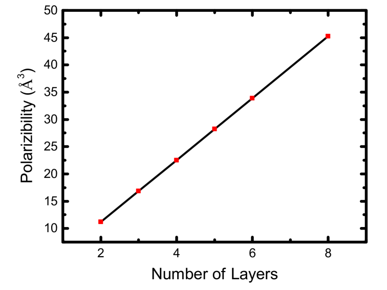
where is the extended supercell volume to include the surface charges which extend beyond the top and bottom atomic phosphorene layers by [see Fig. 4(b), and Eq. (10)]. In Eq. (7), implies which represents a slab of vacuum. Further in Eq. (7), implies , which is the polarizability of a metal slab. In general for an insulator, finite polarizability is proportional to the fraction of the supercell volume that acts like a metal under a transverse electric field. Thus, if the polarizability per atom in phosphorene does not vary much, then the slab polarizability is expected to be a linear function of the number of layers. Note that Eq. (7) is valid only under the assumption that polarization is linearly proportional to the applied electric field, and further that there is no ionic contribution to the local electric field, both of which are likely to be valid only for small values of the applied electric field. We plot the polarizability as a function of the number of layers in Fig. 6 and find that indeed the slab polarizability is a straight line, as expected. Similar linear behaviour of the slab polarizability with the number of layers, has been demonstrated earlier for other two dimensional materials, such as benzene slabs Tóbik and Dal Corso (2004), graphene Yu et al. (2008), GaS Li et al. (2014b) etc.
Following Refs. [Tóbik and Dal Corso, 2004; Yu et al., 2008; Li et al., 2015a], the slab polarizability can also be expressed in terms of the bulk dielectric permittivity of black phosphorus via the relation
| (8) |
where is the volume of the bulk unit cell with two layers, is the dielectric constant of bulk black phosphorus, and is surface polarizability, which captures the difference in the dielectric properties of a slab and bulk. Based on the straight line fit to the slab polarizability data in Fig. 6, we obtain the value of and Å3. Evidently, the surfaces are less polarizable than the bulk. Here we emphasize that the bulk value of the relative permittivity of black phosphorene from the polarizability, is more than that of the actual value of 8.3 Asahina and Morita (1984); Nagahama et al. (1985). This discrepancy of less that in covalent solids, is known to be a direct consequence of simplistic assumption, of a solid being a collection of independently polarizable bi-layers which do not interact with each other, that is used to derive Eq. (8). Similar discrepancy has also been reported earlier for graphene Yu et al. (2008) and Si Giustino and Pasquarello (2005).
Finally we note that Eqs. (7)-(8) can also be combined to predict the dielectric permittivity for any number of layers, once we have the results for a few layers, at least in the low electric field regime where the polarization is expected to be linearly dependent on the external field. Eliminating form Eqs. (7)-(8), we obtain
| (9) |
where
| (10) |
In Eq. (10), is the is the thickness of a single phosphorene layer due to its puckered nature and indicates the interlayer spacing [see Fig. 1], and is the distance between (or ) and the exact supercell boundary i.e. where the bottommost (or topmost) atoms are located, as depicted in Fig. 4(b). Physically indicates the region of charge spillover beyond the outermost atomic layers, and it does not vary significantly with varying number of layers for low electric fields. In Fig. 5(b), we display the predicted effective dielectric constant from Eq. (9) for up-to 20 layers, and evidently it shows a very good match with the actual DFT calculated values.
V Conclusion
To summarize, we have studied the dielectric properties of few layer black phosphorene, using first principle electronic structure calculations and find that (a) in general the relative permittivity increases with increasing number of layers, ultimately saturating to the bulk value, and (b) it can be tuned to a certain extent by an external electric field. The decreasing dielectric constant with reducing number of layers of phosphorene in the low field regime, is a direct consequence of the lower polarizability of the surface layers and the increasing surface to volume ratio.
In addition to the effective dielectric constant, we also calculate the slab polarizability of multilayered black phosphorene, and find that for small electric fields it displays a linear relationship with the number of layers, implying a nearly constant polarization per phosphorus atom as expected. However for large electric fields, which decreases with increasing number of layers, for example V/Å for 6 layers, and V/Å for 4 layers, as per GGA calculations — see Fig. 5(a), this simple relationship breaks down, on account of possible breakdown of the linear relationship between polarization and the applied field, and increasing impact of ionic contribution to the effective field. In the low field regime, one can model the system as a collection of well spaced and independent bi-layer units, and obtain the slab polarizability in terms of the bulk dielectric constant and surface polarizability on one hand, and on the other the slab polarizability can be related to the layer dependent dielectric constant. This allows us to extrapolate our calculations for few layers, to much larger number of layers and obtain an empirical relation for the thickness dependent dielectric constant for any number of layers – see Eq. (9).
Finally we note that all the calculations presented in this article, are valid only for the insulating regime of phosphorene. Further in a realistic experimental scenario, the effective dielectric constant is also likely to be affected by the environment, for example the substrate used, passivation method, etc. and incorporating these effects would require a more detailed numerical study. However our study offers a good starting point, and demonstrates the thickness dependent and electric field tunability of the dielectric constant in phosphorene, which provides an additional handle for optimally designing, and interpreting phosphorene based devices.
References
- Liu et al. (2014) Han Liu, Adam T Neal, Zhen Zhu, Zhe Luo, Xianfan Xu, David Tománek, and Peide D Ye, “Phosphorene: an unexplored 2d semiconductor with a high hole mobility,” ACS nano 8, 4033–4041 (2014).
- Li et al. (2014a) Likai Li, Yijun Yu, Guo Jun Ye, Qingqin Ge, Xuedong Ou, Hua Wu, Donglai Feng, Xian Hui Chen, and Yuanbo Zhang, “Black phosphorus field-effect transistors,” Nature nanotechnology 9, 372–377 (2014a).
- Qiao et al. (2014) Jingsi Qiao, Xianghua Kong, Zhi-Xin Hu, Feng Yang, and Wei Ji, “High-mobility transport anisotropy and linear dichroism in few-layer black phosphorus,” Nature communications 5, 4475 (2014).
- Xia et al. (2014) Fengnian Xia, Han Wang, and Yichen Jia, “Rediscovering black phosphorus as an anisotropic layered material for optoelectronics and electronics,” Nature Communications 5, 4458 (2014).
- Guo et al. (2015) Zhinan Guo, Han Zhang, Shunbin Lu, Zhiteng Wang, Siying Tang, Jundong Shao, Zhengbo Sun, Hanhan Xie, Huaiyu Wang, Xue-Feng Yu, and Paul K. Chu, “From black phosphorus to phosphorene: Basic solvent exfoliation, evolution of raman scattering, and applications to ultrafast photonics,” Advanced Functional Materials 25, 6996–7002 (2015).
- Woomer et al. (2015) Adam H. Woomer, Tyler W. Farnsworth, Jun Hu, Rebekah A. Wells, Carrie L. Donley, and Scott C. Warren, “Phosphorene: Synthesis, scale-up, and quantitative optical spectroscopy,” ACS Nano 9, 8869–8884 (2015).
- Wang et al. (2015a) Xiaomu Wang, Aaron M Jones, Kyle L Seyler, Vy Tran, Yichen Jia, Huan Zhao, Han Wang, Li Yang, Xiaodong Xu, and Fengnian Xia, “Highly anisotropic and robust excitons in monolayer black phosphorus,” Nature nanotechnology 10, 517 (2015a).
- Mao et al. (2015) Nannan Mao, Jingyi Tang, Liming Xie, Juanxia Wu, Bowen Han, Jingjing Lin, Shibin Deng, Wei Ji, Hua Xu, Kaihui Liu, Lianming Tong, and Jin Zhang, “Optical anisotropy of black phosphorus in the visible regime,” Journal of the American Chemical Society 138, 300 (2015).
- Çak ır et al. (2015) Deniz Çak ır, Cem Sevik, and Francois M. Peeters, “Significant effect of stacking on the electronic and optical properties of few-layer black phosphorus,” Phys. Rev. B 92, 165406 (2015).
- Dai and Zeng (2014) Jun Dai and Xiao Cheng Zeng, “Bilayer phosphorene: effect of stacking order on bandgap and its potential applications in thin-film solar cells,” The Journal of Physical Chemistry Letters 5, 1289–1293 (2014).
- Li et al. (2014b) Yan Li, Shengxue Yang, and Jingbo Li, “Modulation of the electronic properties of ultrathin black phosphorus by strain and electrical field,” The Journal of Physical Chemistry C 118, 23970–23976 (2014b).
- Fei and Yang (2014) Ruixiang Fei and Li Yang, “Strain-engineering the anisotropic electrical conductance of few-layer black phosphorus,” Nano letters 14, 2884–2889 (2014).
- Çakır et al. (2014) Deniz Çakır, Hasan Sahin, and François M Peeters, “Tuning of the electronic and optical properties of single-layer black phosphorus by strain,” Physical Review B 90, 205421 (2014).
- Wang et al. (2015b) Can Wang, Qinglin Xia, Yaozhuang Nie, and Guanghua Guo, “Strain-induced gap transition and anisotropic dirac-like cones in monolayer and bilayer phosphorene,” Journal of Applied Physics 117, 124302 (2015b).
- Rastogi et al. (2014) Priyank Rastogi, Sanjay Kumar, Somnath Bhowmick, Amit Agarwal, and Yogesh Singh Chauhan, “Doping strategies for monolayer mos2 via surface adsorption: A systematic study,” The Journal of Physical Chemistry C 118, 30309–30314 (2014).
- Ghosh et al. (2015) Barun Ghosh, Suhas Nahas, Somnath Bhowmick, and Amit Agarwal, “Electric field induced gap modification in ultrathin blue phosphorus,” Phys. Rev. B 91, 115433 (2015).
- Rastogi et al. (2015) P. Rastogi, S. Kumar, S. Bhowmick, A. Agarwal, and Y. Singh Chauhan, “Effective Doping of Monolayer Phosphorene by Surface Adsorption of Atoms for Electronic and Spintronic Applications,” ArXiv e-prints (2015), arXiv:1503.04296 [cond-mat.mes-hall] .
- Nahas et al. (2015) S. Nahas, B. Ghosh, S. Bhowmick, and A. Agarwal, “New ground states of fluorinated and oxidized phosphorene: structural and electronic properties,” ArXiv e-prints (2015), arXiv:1507.07230 [cond-mat.mtrl-sci] .
- Wang et al. (2015c) V. Wang, Y. Kawazoe, and W. T. Geng, “Native point defects in few-layer phosphorene,” Phys. Rev. B 91, 045433 (2015c).
- Dolui and Quek (2015) Kapildeb Dolui and Su Ying Quek, “Quantum-confinement and structural anisotropy result in electrically-tunable dirac cone in few-layer black phosphorous,” Scientific Reports 5, 11699 (2015).
- Liu et al. (2015) Qihang Liu, Xiuwen Zhang, L. B. Abdalla, Adalberto Fazzio, and Alex Zunger, “Switching a normal insulator into a topological insulator via electric field with application to phosphorene,” Nano Letters 15, 1222–1228 (2015).
- Santos and Kaxiras (2013a) Elton JG Santos and Efthimios Kaxiras, “Electric-field dependence of the effective dielectric constant in graphene,” Nano letters 13, 898–902 (2013a).
- Santos and Kaxiras (2013b) Elton JG Santos and Efthimios Kaxiras, “Electrically driven tuning of the dielectric constant in mos2 layers,” ACS nano 7, 10741–10746 (2013b).
- Tóbik and Dal Corso (2004) Jaroslav Tóbik and Andrea Dal Corso, “Electric fields with ultrasoft pseudo-potentials: Applications to benzene and anthracene,” The Journal of chemical physics 120, 9934–9941 (2004).
- Yu et al. (2008) E. K. Yu, D. A. Stewart, and Sandip Tiwari, “Ab initio study of polarizability and induced charge densities in multilayer graphene films,” Physical Review B 77, 195406 (2008).
- Li et al. (2015a) Yan Li, Hui Chen, Le Huang, and Jingbo Li, “Ab initio study of the dielectric and electronic properties of multilayer gas films,” The Journal of Physical Chemistry Letters 6, 1059–1064 (2015a).
- Troullier and Martins (1991) Norman Troullier and José Luís Martins, “Efficient pseudopotentials for plane-wave calculations,” Physical review B 43, 1993 (1991).
- Giannozzi et al. (2009) Paolo Giannozzi, Stefano Baroni, Nicola Bonini, Matteo Calandra, Roberto Car, Carlo Cavazzoni, Davide Ceresoli, Guido L Chiarotti, Matteo Cococcioni, Ismaila Dabo, et al., “Quantum espresso: a modular and open-source software project for quantum simulations of materials,” Journal of Physics: Condensed Matter 21, 395502 (2009).
- Perdew et al. (1996) John P Perdew, Kieron Burke, and Matthias Ernzerhof, “Generalized gradient approximation made simple,” Physical review letters 77, 3865 (1996).
- Klimeš et al. (2010) Jiří Klimeš, David R Bowler, and Angelos Michaelides, “Chemical accuracy for the van der waals density functional,” Journal of Physics: Condensed Matter 22, 022201 (2010).
- Dion et al. (2004) Max Dion, Henrik Rydberg, Elsebeth Schröder, David C Langreth, and Bengt I Lundqvist, “Van der waals density functional for general geometries,” Physical review letters 92, 246401 (2004).
- Thonhauser et al. (2007) Timo Thonhauser, Valentino R Cooper, Shen Li, Aaron Puzder, Per Hyldgaard, and David C Langreth, “Van der waals density functional: Self-consistent potential and the nature of the van der waals bond,” Physical Review B 76, 125112 (2007).
- Román-Pérez and Soler (2009) Guillermo Román-Pérez and José M Soler, “Efficient implementation of a van der waals density functional: application to double-wall carbon nanotubes,” Physical review letters 103, 096102 (2009).
- Sabatini et al. (2012) Riccardo Sabatini, Emine Küçükbenli, Brian Kolb, Timo Thonhauser, and Stefano De Gironcoli, “Structural evolution of amino acid crystals under stress from a non-empirical density functional,” Journal of Physics: Condensed Matter 24, 424209 (2012).
- Bengtsson (1999) Lennart Bengtsson, “Dipole correction for surface supercell calculations,” Physical Review B 59, 12301 (1999).
- Kane and Mele (2005) C. L. Kane and E. J. Mele, “ topological order and the quantum spin hall effect,” Phys. Rev. Lett. 95, 146802 (2005).
- Roy (2009a) Rahul Roy, “ classification of quantum spin hall systems: An approach using time-reversal invariance,” Phys. Rev. B 79, 195321 (2009a).
- Roy (2009b) Rahul Roy, “Topological phases and the quantum spin hall effect in three dimensions,” Phys. Rev. B 79, 195322 (2009b).
- Soluyanov and Vanderbilt (2011) Alexey A. Soluyanov and David Vanderbilt, “Computing topological invariants without inversion symmetry,” Phys. Rev. B 83, 235401 (2011).
- Li et al. (2015b) Yan Li, Hui Chen, Le Huang, and Jingbo Li, “Ab initio study of the dielectric and electronic properties of multilayer gas films,” The Journal of Physical Chemistry Letters 6, 1059–1064 (2015b).
- Giustino and Pasquarello (2005) Feliciano Giustino and Alfredo Pasquarello, “Theory of atomic-scale dielectric permittivity at insulator interfaces,” Physical Review B 71, 144104 (2005).
- Griffiths (1989) D.J. Griffiths, Introduction to electrodynamics (Prentice Hall, New Jersy, USA, 1989).
- Asahina and Morita (1984) H Asahina and A Morita, “Band structure and optical properties of black phosphorus,” Journal of Physics C: Solid State Physics 17, 1839 (1984).
- Nagahama et al. (1985) Toshiya Nagahama, Michihiro Kobayashi, Yuichi Akahama, Shoichi Endo, and Shin ichiro Narita, “Optical determination of dielectric constant in black phosphorus,” Journal of the Physical Society of Japan 54, 2096–2099 (1985).