Electronic correlations in monolayer VS2
Abstract
The layered transition metal dichalcogenide vanadium disulfide (VS2), which nominally has one electron in the shell, is potent for strong correlation physics and is possibly another realization of an effective one-band model beyond the cuprates. Here monolayer VS2 in both the trigonal prismatic and octahedral phases is investigated using density functional theory plus Hubbard (DFT+) calculations. Trigonal prismatic VS2 has an isolated low-energy band that emerges from a confluence of crystal field splitting and direct V–V hopping. Within spin density functional theory, ferromagnetism splits the isolated band of the trigonal prismatic structure, leading to a low-band-gap ferromagnetic Stoner insulator; the octahedral phase is higher in energy. Including the on-site interaction increases the band gap, leads to Mott insulating behavior, and for sufficiently high values stabilizes the ferromagnetic octahedral phase. The validity of DFT and DFT+ for these two-dimensional materials with potential for strong electronic correlations is discussed. A clear benchmark is given by examining the experimentally observed charge density wave (CDW) in octahedral VS2, for which DFT grossly overestimates the bond length differences compared to known experiments; the presence of CDWs is also probed for the trigonal prismatic phase. Finally, we investigate why only the octahedral phase has been observed in experiments and discuss the possibility of realizing the trigonal prismatic phase. Our work suggests trigonal prismatic VS2 is a promising candidate for strongly correlated electron physics that, if realized, could be experimentally probed in an unprecedented fashion due to its monolayer nature.
pacs:
71.15.Mb, 71.27.+a, 71.30.+h, 71.45.LrI Introduction
Transition metal dichalcogenides (TMDCs), composed of layers of chalcogen–metal–chalcogen units (hereto called monolayers) that stack and adhere via weak bonding, are a diverse class of materials known to exhibit charge density waves, metal-insulator transitions, superconductivity, and novel optoelectronic properties.Wilson and Yoffe (1969) Recent breakthroughs in the ability to isolate and manipulate few-layer and monolayer materials, derived from TMDCs like MoS2 and other layered crystals such as graphite, have enabled new possibilities for device applications as well as fundamental studies of low-dimensional systems.Novoselov et al. (2005)
Many TMDCs are nominally (e.g. TiS2) or band insulators in which an even number of electrons completely fills the valence band (e.g. MoS2). Such configurations preclude the possibility of strong electronic correlations and/or magnetism in the ground state. However, there are known examples from experiments of non-oxide layered materials exhibiting magnetism and in some cases insulating behavior. Spin-3/2 CrTe3 is a ferromagnetic insulator with Curie temperature of 33 K for =Si and 61 K for =Ge; monolayers in this class of materials have been predicted to be stable with ferromagnetic exchange as well.Carteaux et al. (1991, 1995); Li and Yang (2014); Sivadas et al. (2015); Zhuang et al. (2015) The spin-1/2 insulator Cr is a ferromagnet below 37 K for =Br and 61 K for =I; in CrCl3 ferromagnetic layers stack in an antiferromagnetic pattern with a Néel temperature of 17 K.de Haas et al. (1940); Tsubokawa (1960); Cable et al. (1961); Dillon Jr. and Olson (1965) Ferromagnetic Fe3GeTe2, which is metallic, has a substantial Curie temperature of 150 K.Deiseroth et al. (2006); Chen et al. (2013) In-plane antiferromagnetism is also observed; MnPS3 and MnPSe3 are spin-5/2 antiferromagnets with Néel temperatures of 78 and 74 K, respectively.Wildes et al. (1998); Jeevanandam and Vasudevan (1999) Additionally, there are numerous antiferromagnets in the family of Fe pnictide superconductors.Dai (2015)
VS2 is an interesting candidate among the many possible TMDCs. Here nominal electron counting indicates that V donates two electrons to each S, leaving it in a (i.e., spin-1/2) configuration. Therefore, VS2 might be potent for strong electronic correlation physics, especially since its electrons will be significantly more localized than the or electrons of NbS2 or TaS2, respectively. Similarly, the electronic states of the sulfur anion should be more localized than those of selenium or tellurium.
The structure of a monolayer TMDC consists of one metal layer sandwiched between two chalcogen layers with each layer corresponding to a triangular lattice. This gives rise to two basic types of chalcogen-metal-chalcogen stacking: ABA stacking, in which the metal layer hosts a mirror plane, or ABC stacking. The latter gives rise to approximate octahedral coordination of the transition metal (TM) by chalcogens, which results in the five-fold manifold splitting into a 3-fold set () and a 2-fold set () of orbitals. More precisely, the octahedral environment experiences a trigonal distortion due to the ability of the chalcogens to relax in the out-of-plane direction. This results in a point group symmetry lowering and a further splitting of the orbitals . For convenience, we refer to the distorted octahedral () phase as the OCT phase in the remainder of this paper.
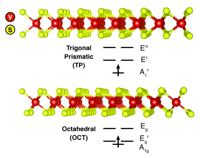
Alternatively, ABA stacking results in a trigonal prismatic (TP) coordination of the TM by the chalcogens. The TP coordination, which is compared to that of the OCT structure in Fig. 1, splits the manifold into a one-fold orbital and two different types of two-fold orbitals ( and ). Both OCT and TP coordinations are possible for VS2, and the TP coordination is particularly intriguing since it could potentially be a physical realization of a one-band model with strong interactions; this rare feature is a hallmark of the copper oxide (cuprate) high-temperature superconductors.Zhang and Rice (1988)
Experimentally the TP phase has not been realized, but bulk VS2 was first synthesized in the OCT phase in the 1970s by deintercalating LiVS2.Murphy et al. (1977) It exhibits a charge density wave (CDW) below K with a wavevector , where is the corner of the Brillouin zone.Murphy et al. (1977); Tsuda et al. (1983); Mulazzi et al. (2010) In the CDW phase Mulazzi et al. found metallic resistivity and no lower Hubbard band in the photoemission spectrum, suggesting rather weak electronic correlations.Mulazzi et al. (2010) Only a very small paramagnetic response was observed in the magnetic susceptibility, which it was suggested might stem from V located in between neighboring VS2 monolayers. A more recent high-pressure synthesis by Gauzzi et al. found much more appreciable local magnetic moments but no long-range CDW, and it was speculated that “nm-size domains” might be responsible.Gauzzi et al. (2014) Using phonon calculations, they also showed that the presence of a CDW soft mode is very sensitive to the lattice parameters. Nanosheets, though not a monolayer, of OCT VS2 have been synthesized and interpreted as showing ferromagnetism.Feng et al. (2011, 2012); Gao et al. (2013); Zhong et al. (2014)
Here we employ first-principles electronic structure calculations based on DFT to explore the physics of VS2. We focus on a single layer of the material since the realization of a strongly correlated monolayer material could enable one to probe Mott physics via gating and strain in an unprecedented way. We find that DFT captures the CDW in OCT VS2 and explains the lack of correlations observed experimentally, though it substantially overestimates the structural distortion. The addition of an appreciable on-site Hubbard interaction to the V site leads to anti-aligned spins in OCT VS2 and yields V–V bond length distortions and metallic behavior in reasonable agreement with known experiments. Unlike the OCT phase, we find that TP VS2 has an isolated low-energy band at the level of non-spin-polarized DFT due to the crystal field and direct V–V hopping. The preferred magnetic order is ferromagnetic, as opposed to the antiferromagnetic ordering found in the cuprates, and this magnetism opens up a small band gap by splitting the band. The on-site interaction leads to a low-band-gap ferromagnetic Mott insulator. For a narrow range of we find evidence for a CDW in TP VS2. Although DFT predicts ferromagnetic TP VS2 is the ground state, for moderate values of we find the OCT structure becomes thermodynamically favored.
II Computational Details
Density functional theory (DFT) Hohenberg and Kohn (1964); Kohn and Sham (1965) calculations within the generalized gradient approximation of Perdew, Burke, and Ernzerhof Perdew et al. (1996) are performed using the Vienna ab initio simulation package (vasp).Kresse and Hafner (1994, 1993); Kresse and Furthmüller (1996a, b) The Kohn-Sham equations are solved using a plane-wave basis set with a kinetic energy cutoff of 500 eV and the projector augmented wave method.Blöchl (1994); Kresse and Joubert (1999) The out-of-plane lattice vector length is chosen to be 20 Å. To sample reciprocal space we employ a -point grid for the primitive unit cell and -point grids with approximately the same -point density for supercells. We utilize the tetrahedron method with Blöchl correctionsBlöchl et al. (1994) for all calculations except for structural relaxations and phonon calculations in metals, for which we employ the first-order Methfessel-Paxton methodMethfessel and Paxton (1989) with a 50 meV smearing. The total energy, ionic forces, and stress tensor components are converged to 10-6 eV, 0.01 eV/Å, and 10-3 GPa, respectively.
To compute maximally-localized Wannier functions (MLWF) we employ the wannier90 code.Mostofi et al. (2008) The rotationally-invariant DFT+ approach with fully localized limit (FLL) double countingLiechtenstein et al. (1995) is used to explore the impact of an on-site Hubbard on the V 3 electrons. Values of on-site Coulomb repulsion are computed from first principles via the linear response approach of Cococcioni and de Gironcoli.Cococcioni and de Gironcoli (2005) We do not employ an on-site exchange interaction since this effect is present within spin density functional theory.Park et al. (2015) We use the direct (supercell) approach in phonopyTogo et al. (2008) to compute phonon dispersion relations. For these calculations we employ a 551 supercell for smaller and a larger 661 supercell for 3 eV, which we find is needed to capture the presence of soft mode instabilities. Phonons at select -points are obtained using the frozen phonon method to assess supercell convergence of direct calculations. Images of crystal structures are generated with vesta.Momma and Izumi (2011)
III Results and Discussion
III.1 CDW in OCT VS2 within DFT
Given that a collection of experiments exist for the bulk OCT phase, we begin by addressing the physics of the OCT monolayer. Since bulk OCT VS2 is known to undergo a CDW transition below K,Murphy et al. (1977); Tsuda et al. (1983); Mulazzi et al. (2010) we explore the presence of such a CDW in the monolayer OCT structure. We compute the phonon frequencies using the frozen phonon method for , the experimental CDW wavevector from electron microscopy,Mulazzi et al. (2010) and verify the soft mode in the non-spin-polarized (NSP) bulk OCT phase as found in a previous study.Gauzzi et al. (2014) We find the frequency is cm-1. For the monolayer, at this wavevector we find the same soft mode in the NSP state now with a slightly softer frequency cm-1. Given the experimental CDW wavevector is in-plane and the similarity of the soft mode for the bulk and the monolayer, we expect the monolayer CDW to be representative of that of the bulk. Additionally, at a slightly different wavevector of we find a soft mode of smaller magnitude cm-1 in the monolayer.
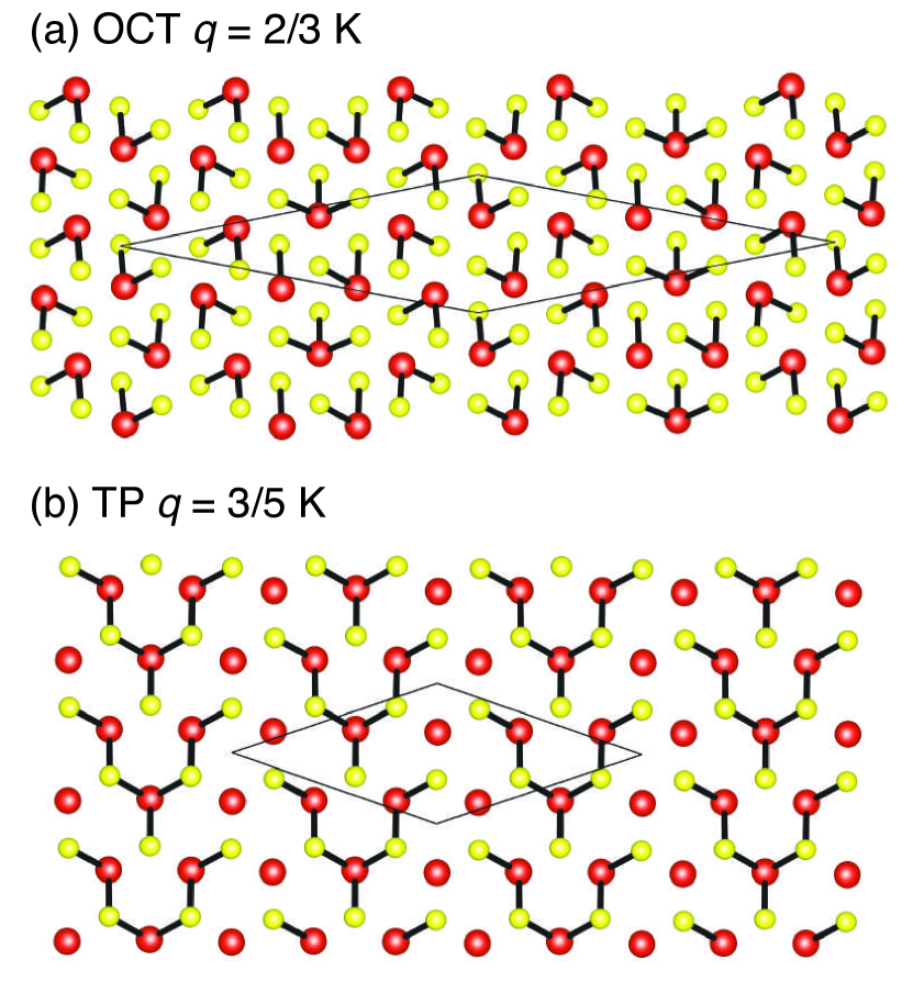
Without any CDW the lowest-energy state of monolayer OCT VS2 is a ferromagnetic (FM) metal with a V magnetic moment of 0.5 , which is 13 meV lower in energy than the NSP state. The relaxed NSP OCT CDW state is 12 meV lower in energy than the pristine (without-CDW) FM state. Although we find no soft mode for the pristine OCT FM structure, performing a further structural relaxation of the NSP OCT CDW structure with FM initialization leads to an additional small (<1 meV) energy lowering (see Fig. 5). In this structure, depicted in Fig. 2(a), distinct V sites have one, two, or three nearest-neighbor S atoms instead of the six of the pristine OCT structure. The CDW has substantially suppressed the V magnetic moments to 0.0–0.2 , which is consistent with the weak correlations observed by Mulazzi et al. However, the V–S and V–V bond lengths exhibit massive variations of 2.2–2.6 and 3.0–3.7 Å , respectively. The range of V–V bond lengths deduced by Sun et al. via x-ray absorption fine spectroscopy (XAFS) is only 0.19 Å.Sun et al. (2015) Therefore, DFT is severely overestimating the structural deformation in the CDW state and beyond-DFT approaches will be necessary to describe the OCT CDW phase; we address this point in detail using DFT+ in Sec. III.4. Also, additional experimental studies would be helpful to understand the lack of long-range CDW found using high-pressure synthesis.
III.2 Non-spin-polarized DFT electronic structure
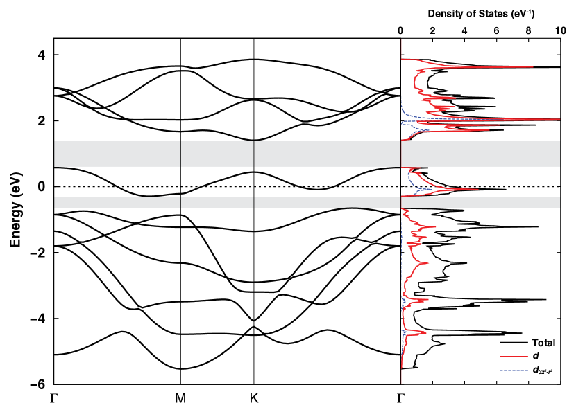
The NSP band structure and density of states for TP VS2 are shown in Fig. 3. We do find an isolated low-energy band like in the crystal field picture shown in the top panel of Fig. 1, but there is a major difference with the simple schematic. The projected density of states shows this isolated band is mainly of character, while the unoccupied manifold above it has slightly less predominant character (i.e., stronger hybridization with S ); the manifold below is predominantly S with some hybridization with V . However, projecting the V density of states onto just the orbital () reveals the main discrepancy with the simple schematic: the isolated band is only roughly half character and the remaining half is character. This puzzle was first noted by Kertesz and Hoffman in the context of TMDCs several decades ago.Kertesz and Hoffmann (1984)
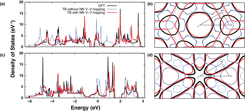
In order to resolve this anomaly and to gain further insight into the electronic structure of the TP phase, we compute MLWF for the full - manifold of TP VS2, which results in atom-centered V -like and S -like orbitals. The Hamiltonian is represented in the MLWF basis, and we explore the impact of removing various matrix elements in the Hamiltonian corresponding to V–S and V–V hoppings; S–S hoppings are always retained. A similar analysis is performed for the OCT phase for comparison.
Panels (a) and (c) of Fig. 4 show the density of states from the MLWF Hamiltonian for NSP TP and OCT VS2 (black curves), respectively, which are identical to those of DFT by construction. The OCT structure, unlike the TP structure, does not have an isolated low-energy band since the crystal field splitting of the into and is relatively weak as is also typical for oxides in this structure. Now we examine the tight binding (TB) approximation in which we remove all V–S and V–V matrix elements beyond nearest neighbor (NN) (thick red lines). In both phases, we qualitatively reproduce all of the gaps and other prominent features of the spectra. For both structures, we find V–V hopping beyond NN is negligible, and therefore all of the quantitative deviation between the black and the red curves is due to V–S hopping beyond NN.
If we only include NN V–S hoppings and no NN V–V hoppings (thin blue lines) one still captures the qualitative features of the spectra for the OCT structure, though there are now large quantitative differences. However, for TP phase there is a qualitative change: there is no longer a gap between the isolated band and the higher-energy bands. Therefore, the V–V hopping plays a strong contribution in splitting off the isolated band. Furthermore, it addresses the observation presented by Kertesz and Hoffman. The fact that the NN V–V hoppings have a strong interorbital component explains why only contributes half of character of the isolated band. Interestingly, we also find that the rapid decay of these direct TM–TM hoppings with strain explains the semiconductor-to-semimetal transition in the isostructural material MoS2 under strain.Scalise et al. (2012)
Panels (b) and (d) of Fig. 4 illustrate the Fermi surfaces of the TP phase and OCT phase, respectively. In DFT, the Fermi surface of the TP structure has hole pockets centered at and , while that of the OCT structure has a single cigar-shaped electron pocket centered at . For the OCT structure the TB approximation is sufficient to properly capture the Fermi surface topology, but for the TP structure this is not the case and longer-range V–S hopping is needed.
At this level of theory we predict an isolated low-energy band in the TP phase, but as discussed in the next section there is a ferromagnetic instability once spin polarization is included even at the DFT level. This strongly suggests electronic correlations will be important in the TP phase of this material, which therefore is our focus for the remainder of this paper.
III.3 DFT energy level diagram
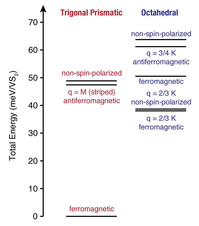
The total energy of different structures and magnetic configurations of monolayer VS2 within DFT is shown in Fig. 5. For the NSP states, the TP structure is lower in energy than the OCT structure by 15 meV. For both structures, the formation of a FM state results in a significant energy lowering compared to the NSP state. The magnitude of the energy decrease is 13 meV for OCT and 49 meV for TP. In the FM state, V in the TP structure is fully spin polarized with a magnetic moment of 1.0 whereas for the OCT structure the moment is only 0.5 , indicating that the TP phase exhibits stronger signatures of electronic correlations. For the OCT phase one must also consider the CDW phase, which lowers the OCT energy by 12 meV compared to the FM state and greatly weakens the magnetism giving moments of only 0.0–0.2 . Ultimately, the TP FM state is the ground state since it is still far lower in energy (38 meV) than the OCT FM CDW phase. The only remaining task is to provide evidence that there are no other magnetic or phonon instabilities.
To confirm the exchange is FM in VS2, we also investigate and antiferromagnetic (AFM) configurations. For the TP phase, only the striped () AFM configuration is found to converge. This metastable state is metallic with small V magnetic moments of 0.2 and is only 1.4 meV lower in energy than the NSP state. Therefore, TP VS2 strongly prefers ferromagnetism and we interpret it as a “Stoner insulator” rather than a Mott insulator at the level of spin-dependent DFT, given that a gap does not persist for an arbitrary magnetic ordering. For the OCT structure a metastable AFM configuration is found only 2.4 meV lower in energy than the NSP state, and it similarly is metallic with small V moments of 0.4 . The FM nature of the exchange in this system is not unexpected since the V–S–V angle is 84–85 degrees, close to the 90-degree ferromagnetism given by the Goodenough-Kanamori rules.Goodenough (1955, 1958); Kanamori (1959)
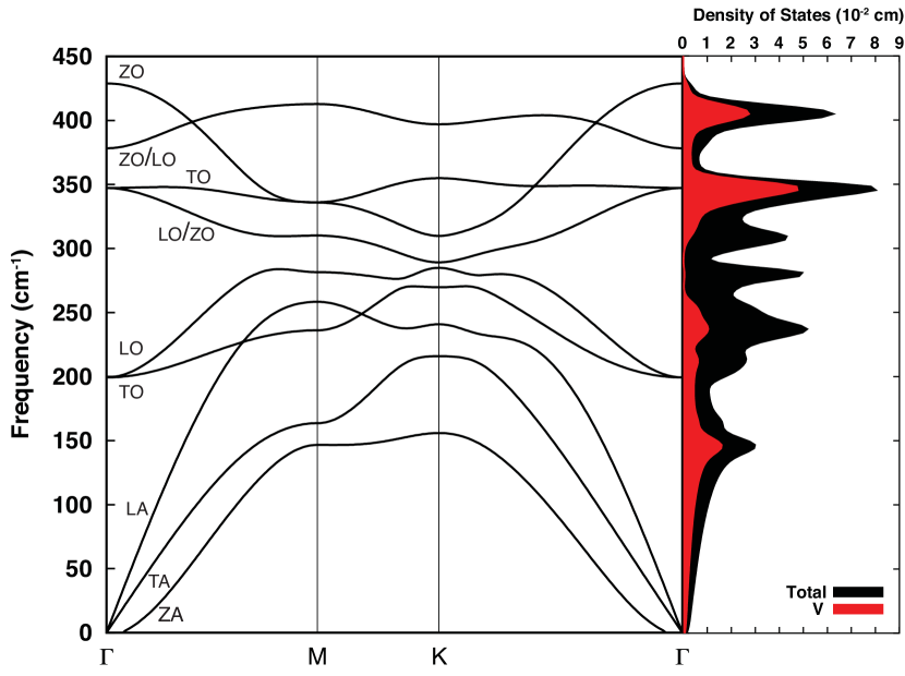
We compute the phonon dispersion and density of states of FM TP VS2, shown in Fig. 6, to assess the dynamic stability of this phase. The out-of-plane acoustic (za) branch has the form near characteristic of two-dimensional materials. There is no frequency gap between the acoustic and optical branches. The out-of-plane optical (zo) branches are the highest-frequency phonons. Since there are no modes with imaginary frequency, this phase is stable at the level of DFT.
The above analysis of the magnetism and the phonons allows us to conclude that the FM TP phase is the ground state within DFT. One would not interpret this as a Mott insulator within DFT given that the band gap does not persist for all spin configurations.
III.4 Impact of on-site Hubbard
We use the linear response approachCococcioni and de Gironcoli (2005) to estimate the correlation strength for V in VS2. Computing screened interactions for use in beyond-DFT methods is still an active area of research, but the linear response approach is useful to set a baseline for the expected value of . For FM states, we obtain eV for the TP phase and eV for OCT phase. For the TP phase, we also compute the for the NSP state and obtain 4.14 eV. These values are generally smaller than oxides of vanadiumXu et al. (2015) and larger than sulfides of titanium and tantalum.Sánchez et al. (2008); Darancet et al. (2014) Ultimately, one still needs to carefully investigate the effect of on the physical observables given the methodological uncertainties.
| (eV) | E (meV) | V–S bond length range (Å) | V magnetic moment range () | |
|---|---|---|---|---|
| NSP | 0 | -17 | 2.22–2.52 | — |
| 1 | -20 | 2.23–2.51 | — | |
| 2 | -33 | 2.24–2.51 | — | |
| 3 | -60 | 2.25–2.51 | — | |
| NSP | 0 | -25 | 2.18–2.57 | — |
| 1 | -27 | 2.20–2.56 | — | |
| 2 | -34 | 2.21–2.55 | — | |
| 3 | -60 | 2.25–2.52 | — | |
| FM | 0 | -7 | 2.21–2.53 | 0.03–0.38 |
| 1 | -2 | 2.30–2.42 | 1.17–1.19 | |
| 2 | -14 | 2.26–2.51 | 1.21–1.39 | |
| 3 | -1 | 2.37–2.42 | 1.30–1.40 | |
| FM | 0 | -12 | 2.18–2.57 | -0.02–0.18 |
| 1 | -12 | 2.26–2.47 | 1.14–1.20 | |
| 2 | -10 | 2.27–2.49 | 1.27–1.32 | |
| 3 | -1 | 2.39–2.40 | 1.28–1.33 |
Another useful benchmark that could provide a bound for is the CDW in the OCT phase. We performed structural relaxations to check if the CDW is still captured for finite . The total energy lowering E, V–S bond length range, and V magnetic moment range for the relaxed structures are given in Table 1 for NSP and FM OCT VS2 for and . For the NSP states the energy lowering from the CDW increases substantially with and is 60 meV for eV. For the FM states, the CDW persists for moderate values of but it is substantially dampened once is 3 eV with a total energy lowering of only 1 meV. However, at we find evidence for a new CDW ground state with AFM-like correlations. This system is a ferrimagnetic metal with 2 V moments of 1.3 , 3 V moments of 1.4 , and 4 V moments of -1.2 . We refer to it as an AFM state for simplicity since the total magnetization is only 0.21 per formula unit.
Further evidence for this tendency for AFM correlations in OCT VS2 for larger comes from calculations of the and AFM states. For eV the and AFM states are also lower in energy than the pristine FM state by 29 and 19 meV, respectively. The AFM CDW state is even lower in energy, 39 meV lower than the pristine FM state, and therefore is the ground state. For eV this trend persists as and phases with anti-aligned magnetic moments are lower in energy than the pristine FM phase by 35 and 29 meV, respectively. It should be emphasized that these anti-aligned magnetic states are strongly coupled to the structural distortions; performing an unrelaxed eV calculation based on the FM or eV relaxed structure of the primitive unit cell (i.e., without any CDW) demonstrates that the FM spin ordering persists as the ground state.
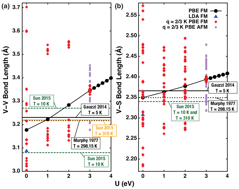
To assess which regime of best agrees with experiments on the CDW phase, we compare the V–V and V–S bond lengths of our calculated structures to those of known experiments in Fig. 7. For the V–V bond length the high-temperature value of Sun et al. agrees well with that of Murphy et al., which may be reasonable since the temperature is approaching the CDW transition at 305 K. Gauzzi et al., who do not find a long-range CDW, observe a slightly larger V–V bond length at low temperature. The work of Sun et al. is the only one that presents bond lengths at low temperature well within the CDW phase; they report a V–V bond length difference of 0.19 Å.
Applying DFT+ while not allowing spontaneously broken translational symmetry, the V–V and V–S bond lengths of the pristine FM state increase roughly linearly with . For this state, within DFT () PBE predicts larger bond lengths than the local density approximation (LDA) as is typical. As discussed in Sec. III.1, for the range of V–V bond lengths of the FM CDW phase (0.70 Å) is over 3.5 times the low-temperature XAFS measurement from Sun et al. For and 2 eV the range we compute is smaller but still over twice the experimental value, while the range collapses to only 0.04 Åfor eV. Alternatively, reasonable agreement with experiment occurs for the eV AFM CDW phase. This phase still contains an appreciable CDW distortion, unlike the corresponding FM phase, and the range of V–V bond lengths of 0.28 Å is comparable to that in experiment. Furthermore, the metallic nature of this phase (unlike the gapped FM CDW phase) is qualitatively consistent with the experimental resistivity.Murphy et al. (1977); Mulazzi et al. (2010); Sun et al. (2015) Therefore, an appreciable value of around 3 eV may be most reasonable for OCT VS2, and we find evidence for AFM correlations in this regime. The V–S bond lengths show a similar trend: the eV FM CDW phase exhibits a massive range of values for that is dampened for and 2 eV and nearly disappears for eV. We note that Sun et al. reports only a single temperature-independent V–S bond length, however. A detailed structural refinement from experiment would be instrumental for a more stringent evaluation of available first-principles methodologies.
DFT+ corresponds to a Hartree-Fock (mean-field) solution to the quantum impurity problem of dynamical mean-field theory.Georges et al. (1996); Kotliar et al. (2006) Given the manner in which Hartree-Fock tends to overemphasize the effects of interactions, it would not be surprising to require a smaller value of relative to that of linear response to provide a proper description. Especially given that there are currently no experiments for the TP phase, the above analysis indicates the need to explore a range of values in what follows.
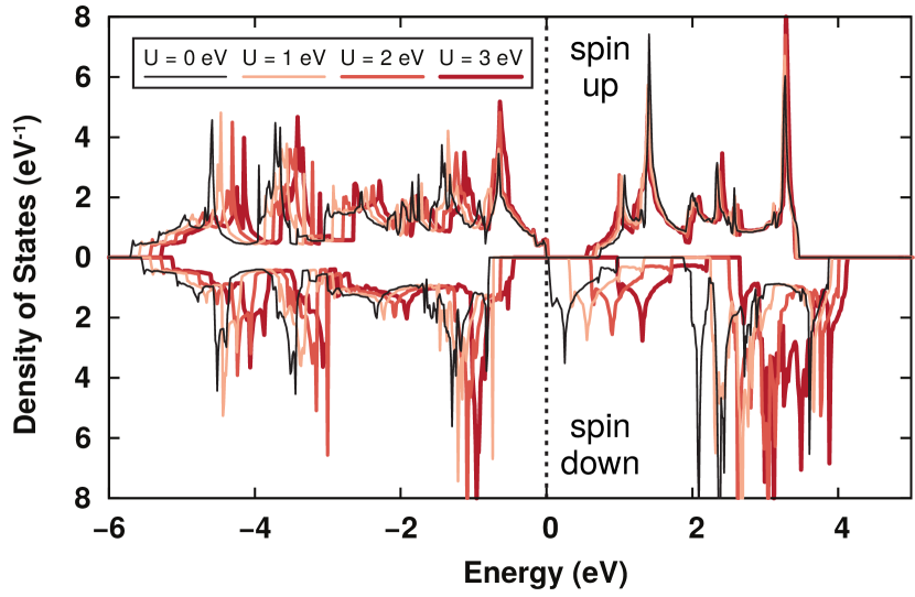
We explore the effect of on the electronic spectrum of FM TP VS2 using DFT+. As shown in Fig. 8, for already there is a small band gap of 30 meV generated by the exchange splitting of the state. With increasing the spin-down state is shifted up in energy, which increases the band gap up to 0.6 eV; the band gap saturates once the spin-up levels become the lowest unoccupied states. This value is somewhat smaller than the 1.1 eV band gap obtained via hybrid functional calculations, which is presumably due to the nonlocality of the potential in the hybrid functional.Huang et al. For small , the -induced energy shift of correlated orbital with occupancy takes the form within DFT+, so one expects an occupied state () to shift down in energy by and an unoccupied state () to shift up in energy by . In this case, however, the spin-up levels are significantly hybridized such that their occupancies are very close to 1/2 (i.e., 0.45–0.48) within DFT. This necessitates that the spin-up manifold is essentially fixed in energy for small . The trend happens to persist over the full range of shown, which is responsible for the band gap saturation observed here as well as in a previous study.Huang et al.
For of 2 and 4 eV the metastable striped AFM configuration is 115 and 66 meV higher in energy than the FM state with a band gap of 0.1 and 0.7 eV and V magnetic moments of 0.6 and 1.3 , respectively. The insulating behavior for this higher-energy magnetic configuration indicates that the system has been driven into a regime of Mott physics, as crudely interpreted from DFT+; this is in contrast to the DFT description in terms of a Stoner instability.
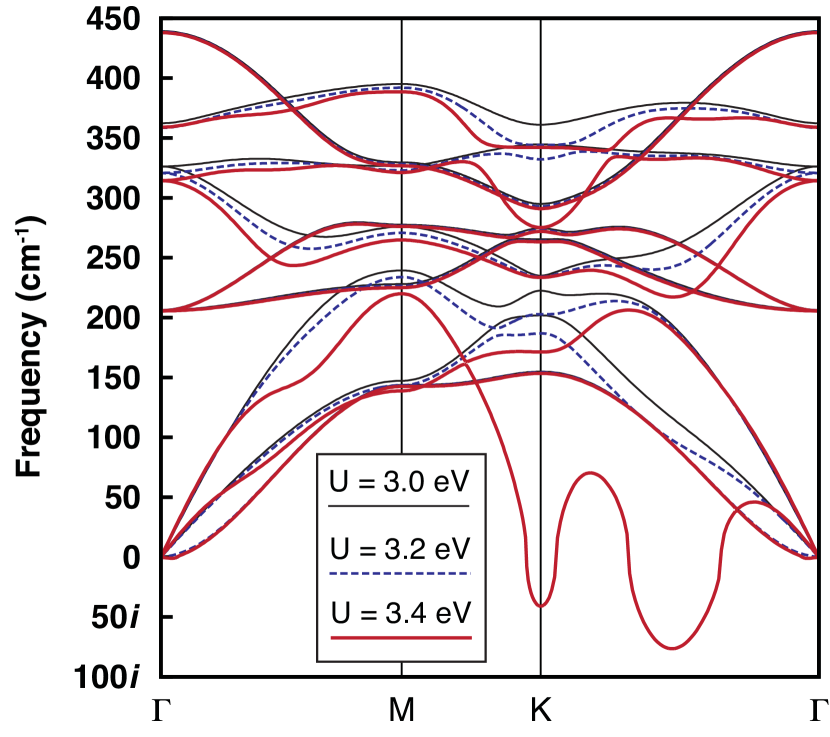
We also examine the impact of on the phonon dispersion relation of the FM TP state to assess the dynamical stability of VS2. Figure 9 illustrates the main result. For eV the phonons are all still stable, as in the DFT case. For eV one can observe the formation of a small dip in the ta branch between and . Once is equal to 3.4 eV, a soft mode is formed. There is an additional soft mode at whose eigenvalue is smaller in magnitude.
| (eV) | E (meV) | V–S bond length range (Å) | V magnetic moment range () | |
|---|---|---|---|---|
| 3.4 | -0.1 | 2.38–2.40 | 1.38–1.39 | |
| 3.6 | -3 | 2.38–2.40 | 1.41–1.41 | |
| 3.8 | -10 | 2.38–2.41 | 1.44–1.44 | |
| 4.0 | +9 | 2.38–2.43 | 1.32–1.50 | |
| 4.2 | +16 | 2.38–2.44 | 1.33–1.52 | |
| 3.4 | -1 | 2.37–2.42 | 1.17–1.56 | |
| 3.6 | -7 | 2.37–2.44 | 1.16–1.71 | |
| 3.8 | -19 | 2.36–2.45 | 1.18–1.82 | |
| 4.0 | -34 | 2.36–2.46 | 1.19–1.90 | |
| 4.2 | -45 | 2.36–2.47 | 1.20–1.97 |
To corroborate and refine our finding of -induced soft modes in the TP phase, we performed frozen phonon calculations at several -points. The frozen phonon method removes the possibility of image interactions, which can cause errors in the supercell approach. For eV we find a 130 cm-1 soft mode at the point, a 100 cm-1 soft mode at , and a 188 cm-1 soft mode at ; this reveals that the supercell approach is qualitatively correct but with substantial quantitative errors.
We performed structural relaxations for the two wavevectors with the softest phonon modes, and , using supercells commensurate with those wavevectors. The total energy lowering E, V–S bond length range, and V magnetic moment range for the relaxed structures are given in Table 2. For eV no structural distortion is found for either wavevector. With larger values, the relaxed structures exhibit lower total energy and modulation of V–S bond lengths and V magnetic moments. For the magnitude of E increases monotonically from 1 meV to 45 meV as increases, corresponding to an enhanced CDW. The V–S bond lengths vary by as much as 0.09 Å and the V magnetic moments differ by as much as 0.8 at a given . For 3.4 eV 3.8 eV the soft mode also shows an appreciable but smaller energy lowering ( meV) with significantly smaller magnitudes of the differences in V–S bond length (0.03 Å) and V magnetic moment (0.01 ); for eV this CDW state becomes higher in energy than the undistorted FM state. For eV we do not find a stable (or even metastable) or CDW state, indicating the prediction of a CDW state for TP VS2 only exists within a narrow window of values.
For eV, both the and soft modes disappear (not pictured). Frozen phonon calculations indicate that the smallest phonon frequency at eV is 126 cm-1 for , 97 cm-1 for , and 79 cm-1 for . In this regime of 4 eV eV we find that the CDW phase is a separate lower-energy state that exists in addition to the metastable undistorted FM state.
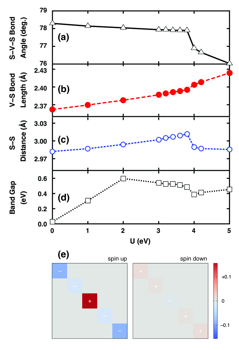
The disappearance of the soft modes at eV appears to be related to a separate electronic and structural phase transition that occurs within the primitive cell of FM TP VS2. To describe the phase transition, we plot in Fig. 10 several structural parameters (out-of-plane S–V–S bond angle, V–S bond length, and out-of-plane S–S distance) and the band gap as a function of for FM TP VS2. There is a sharp discontinuity in the structural parameters at eV that most noticeably leads to decreases in S–V–S bond angle and out-of-plane S–S distance. The band gap shows a discontinuity and begins to decrease at eV when the level is no longer the lowest unoccupied state. At eV there is a slight drop in band gap due to the phase transition, after which it begins to increase roughly linearly. Using the relaxed crystal structure from eV, we are able to converge a eV DFT+ calculation to a metastable state 6 meV higher in energy whose electronic properties (e.g. density of states and local density matrix) resemble those of lower (i.e., eV) as opposed to this new ground state. This, along with the presence of discontinuities in the structural and electronic properties, indicates that the phase transition is of first order.
To better understand the electronic aspect of the phase transition, in Fig. 10(e) we plot the difference in the V on-site density matrices (ground state minus metastable state) obtained using the same crystal structure. The most significant changes occur in the spin-up channel. Compared to the metastable state, in this spin channel the ground state has 0.16 additional occupancy of the () state and 0.16 less in total occupancy of the ( and ) states.
Given the crude nature of DFT+, one must view these results with caution. More advanced calculations using DFT+DMFT, in addition to experiments, would be needed to judge the veracity of this predicted CDW. A smaller value of might be more relevant in VS2 to compensate for errors associated with Hartree-Fock treatment of the impurity problem.
III.5 DFT+ relative phase stability
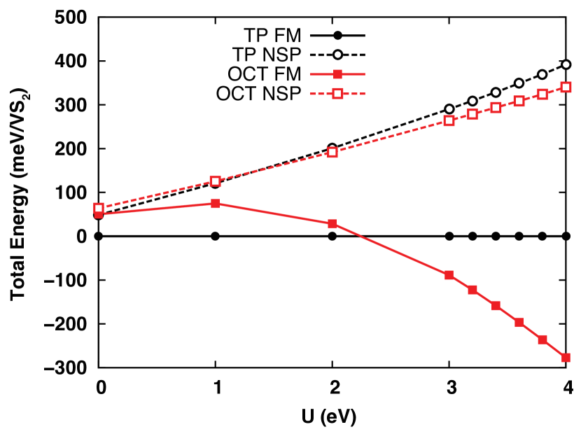
To explore the impact of on the relative energetics of the TP and OCT phases, in Fig. 11 we show the total energy of the NSP and FM states for TP and OCT VS2 referenced to the TP FM state energy. Here the CDWs are not considered as they do not change the qualitative results; all calculations are in the primitive cells. For the TP FM state is the ground state with the TP NSP, OCT FM, and OCT NSP states 49, 50, and 64 meV higher in energy, respectively. As increases the NSP states are each monotonically destabilized by several hundreds of meV compared to the TP FM state as expected. The OCT FM phase has a more complicated nonmonotonic behavior, initially slightly increasing its relative energy with and then decreasing its relative energy for eV. For values larger than 1 eV the OCT FM state becomes an insulator with the state fully polarized (V magnetic moment of 1 ) and is energetically stabilized; for eV it is lower in energy than the TP FM state by 88 meV, and the energy stabilization increases upon further increasing .
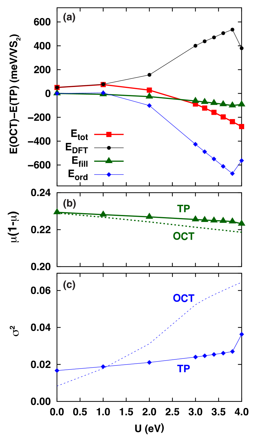
To gain further insight into the stabilization of FM OCT over FM TP VS2 with , we introduce a new spectral decomposition of the DFT+ energy functional into contributions from DFT (), filling of V orbitals (), and ordering of V orbitals ():
where is the angular momentum ( for electrons) and and are the mean and standard deviation of the eigenvalues of the local density matrix. The filling and ordering terms added together give the standard interaction and double counting terms in DFT+ for set to 0. This decomposition provides a convenient way to isolate and quantify the contributions of the average filling of the shell and the spin and orbital ordering of the shell to the interaction and double counting energetics. The former elucidates the energetics associated with moving charge into or out of the correlated subspace, while the latter is the means by which Hartree-Fock captures the energetics of electronic correlations.
As shown in Fig. 12(a), for eV (black circles) and (blue diamonds) are responsible for the further stabilization of the TP phase compared to . For larger , the term (green triangles) increasingly favors the OCT phase by as much as 101 meV as increases. The total E(OCT)–E(TP) (red squares) decreases with a factor of 3 to 4 faster than . and tend to oppose each other, but overall the negative term is dominant and this contributes significantly to the overall stabilization of the OCT phase. The and terms increase in magnitude significantly faster once the OCT phase becomes an insulator at eV. We find the same qualitative behavior when we freeze the ions at the structures, indicating this is not an effect of structural relaxation.
The filling factor and the ordering factor are plotted for both phases in Fig. 12(b) and Fig. 12(c), respectively. Interestingly, the TP and OCT phases have an almost identical filling of the V shell with at . On the other hand, the terms are substantially different at : is 0.0167 in the TP phase as opposed to only 0.0083 in the OCT phase. This stems from the complete spin polarization of the state in the TP phase, as opposed to the partial spin polarization in the OCT phase. The preceding statement can be supported by investigating the NSP state for both the TP and OCT phases for , which yields much more similar values of 0.0037 and 0.0047, respectively. Therefore, the pure crystal fields in each respective case results in a similar and small , while the differing degrees of spin polarization are responsible for the large initial difference at . This enhanced spin ordering in the TP phase leads to the enhanced stabilization of the TP phase in the limit of small since and because the initial fillings are nearly identical. However, this trend is only guaranteed for small and as we pointed out above the trend reverses for eV. We therefore proceed to examine each contribution as a function of . In terms of the filling contribution, the OCT phase filling factor decreases with twice as fast as it does for the TP phase for eV. The for the OCT phase increases 5.2 times as fast as does that of the TP phase for eV, since both the and the states are polarizable, and for eV it has an ordering factor 2.3 times as large. Therefore, both the decreased filling and increased ordering of the orbitals of the OCT phase contribute to its stabilization for larger .
III.6 Possibility of realizing TP VS2
Only the OCT phase of VS2 has been observed experimentally, in bulk and nanosheet forms.Murphy et al. (1977); Feng et al. (2011, 2012); Zhong et al. (2014); Gauzzi et al. (2014) DFT predicts the TP phase is the thermodynamic ground state, while DFT+ predicts that the OCT phase becomes the ground state when surpasses a moderate value of approximately eV. More advanced calculations, including DFT+DMFT and possibly cluster extensions of DMFT, will be needed to definitively settle this issue from a theoretical standpoint. Given that TP may in fact be the ground state, or possibly a metastable state sufficiently low in energy to be achieved experimentally, we explore possible reasons why it has not been observed in experiment.
The initial synthetic route to VS2 was delithiation from LiVS2.Murphy et al. (1977) This lithiated compound has a layered octahedral structure.van Laar and Ijdo (1971) Therefore, one possibility is that VS2 is stuck in a metastable OCT state. Within DFT, we compute an energy barrier of 0.69 eV per formula unit based on a linear interpolation between the TP and OCT monolayer structures allowing only out-of-plane ionic relaxation. This value is in agreement with nudged elastic band calculations that found a barrier of 0.66 eV.Zhang et al. (2013) The large barrier supports the possibility that it could very challenging to change phases. Another high-temperature synthesis technique did not use LiVS2 but still resulted in the OCT phase.Ohno et al. (1982, 1983) One possibility is that finite temperature plays a role in destabilizing the TP phase since there is evidence that the phonon entropy is greater for the OCT phase.Zhang et al. (2013)
A more recent high-pressure synthesis of VS2 also yielded the OCT phase.Gauzzi et al. (2014) We performed spin-polarized DFT (i.e., ) calculations of bulk VS2 under pressure and find that for sufficiently high pressure the OCT phase becomes the ground state, so this could be responsible for why the TP phase is not observed. In these calculations we considered 2Hc (MoS2-like) stackingKatzke et al. (2004) for the TP phase and O1 (CoO2-like) and O3 (LiCoO2-like) stackingsvan der Ven et al. (1998) for the OCT phase. At 5 GPa the TP phase is still the ground state but only 15 meV lower in energy compared to 50 meV for 0 GPa. At 10 GPa the TP phase becomes 26 meV higher in energy than the OCT phase. Based on these observations, if the TP phase is the ground state we predict that synthesis under ambient pressure, low temperature, and not involving a LiVS2 precursor will be most effective to attempt to realize TP VS2.
IV Conclusions
We have demonstrated that monolayer TP VS2 has an isolated low-energy band at level of NSP DFT, which arises due to a combination of the TP crystal field and the nearest-neighbor V–V hopping. Including spin polarization reveals that the exchange is ferromagnetic and yields a FM insulator with a small band gap. Other spin configurations result in metallic states substantially higher in energy, indicating that spin-dependent DFT is not putting VS2 in the Mott regime. While TP VS2 has not been observed in experiment in any form, spin-polarized DFT does predict it is lower in energy than the OCT phase. DFT captures the known CDW in the OCT phase, which strongly diminishes the magnetism relative to the undistorted phase. However, DFT appears to grossly overestimate the CDW amplitude in this phase. Specifically, the V–V bond length differences from DFT are far larger than those of the existing XAFS study.Sun et al. (2015)
Accounting for local correlations via DFT+ produces a FM insulating state in the TP phase, which is in the Mott regime for moderate values of . For a small regime of finite , we find a CDW in the TP phase at . For the OCT phase, increasing diminishes the amplitude of the CDW. For the ferromagnetic CDW state, the amplitude decreases slowly before rapidly collapsing near eV. However, for this regime of , magnetism with anti-aligned spins becomes energetically favored over ferromagnetism. In this magnetic configuration we find metallic behavior as in experiments and the V–V bond length differences of the CDW phase are within reasonable comparison to XAFS experiments.
Regarding relative phase stability, above a reasonably small (approx. 2.3 eV) the energy ordering of TP and OCT phases reverses with the OCT phase becoming the ground state. More advanced calculations, including DFT+DMFT and possibly cluster extensions of DMFT, will be needed to settle which is the ground state structure and determine whether the CDW in the TP phase is physical.
If the TP phase can be realized, it has the potential for novel physics: it would be a rare example of a Mott insulator on a triangular lattice with strong FM correlations. Its monolayer nature might enable doping via gating, allowing one to probe the doped Mott insulator in a precise fashion without simultaneously introducing disorder.
Acknowledgements.
This research used resources of the National Energy Research Scientific Computing Center, a DOE Office of Science User Facility supported by the Office of Science of the U.S. Department of Energy under Contract No. DE-AC02-05CH11231. The authors acknowledge support from the NSF MRSEC program through Columbia in the Center for Precision Assembly of Superstratic and Superatomic Solids (DMR-1420634). E.B.I. gratefully acknowledges support from the U.S. Department of Energy Computational Science Graduate Fellowship (Grant No. DE-FG02-97ER25308).References
- Wilson and Yoffe (1969) J. Wilson and A. Yoffe, Adv. Phys. 18, 193 (1969).
- Novoselov et al. (2005) K. S. Novoselov, D. Jiang, F. Schedin, T. J. Booth, V. V. Khotkevich, S. V. Morozov, and A. K. Geim, Proc. Nat. Acad. Sci. U.S.A. 102, 10451 (2005).
- Carteaux et al. (1991) V. Carteaux, G. Ouvrard, J. C. Grenier, and Y. Laligant, J. Magn. Magn. Mater. 94, 127 (1991).
- Carteaux et al. (1995) V. Carteaux, D. Brunet, G. Ouvrard, and G. Andre, J. Phys.: Condens. Matter 7, 69 (1995).
- Li and Yang (2014) X. Li and J. Yang, J. Mater. Chem. C 2, 7071 (2014).
- Sivadas et al. (2015) N. Sivadas, M. W. Daniels, R. H. Swendsen, S. Okamoto, and D. Xiao, Phys. Rev. B 91, 235425 (2015).
- Zhuang et al. (2015) H. L. Zhuang, Y. Xie, P. R. C. Kent, and P. Ganesh, Phys. Rev. B 92, 035407 (2015).
- de Haas et al. (1940) W. J. de Haas, B. H. Schultz, and J. Koolhaas, Physica 7, 57 (1940).
- Tsubokawa (1960) I. Tsubokawa, J. Phys. Soc. Jpn. 15, 1664 (1960).
- Cable et al. (1961) J. W. Cable, M. K. Wilkinson, and E. O. Wollan, J. Phys. Chem. Solids 19, 29 (1961).
- Dillon Jr. and Olson (1965) J. F. Dillon Jr. and C. E. Olson, J. App. Phys. 36, 1259 (1965).
- Deiseroth et al. (2006) H.-J. Deiseroth, K. Aleksandrov, C. Reiner, L. Kienle, and R. K. Kremer, Eur. J. Inorg. Chem. 2006, 1561 (2006).
- Chen et al. (2013) B. Chen, J. Yang, H. Wang, M. Imai, H. Ohta, C. Michioka, K. Yoshimura, and M. Fang, J. Phys. Soc. Jpn. 82, 124711 (2013).
- Wildes et al. (1998) A. R. Wildes, B. Roessli, B. Lebech, and K. W. Godfrey, J. Phys.: Condens. Matter 10, 6417 (1998).
- Jeevanandam and Vasudevan (1999) P. Jeevanandam and S. Vasudevan, J. Phys.: Condens. Matter 11, 3563 (1999).
- Dai (2015) P. Dai, Rev. Mod. Phys. 87, 855 (2015).
- Zhang and Rice (1988) F. C. Zhang and T. M. Rice, Phys. Rev. B 37, 3759 (1988).
- Murphy et al. (1977) D. W. Murphy, C. Cros, F. J. Di Salvo, and J. V. Waszczak, Inorg. Chem. 16, 3027 (1977).
- Tsuda et al. (1983) T. Tsuda, H. Yasuoka, Y. Kitaoka, and F. J. Di Salvo, J. Magn. Magn. Mater. 31–34, 1101 (1983).
- Mulazzi et al. (2010) M. Mulazzi, A. Chainani, N. Katayama, R. Eguchi, M. Matsunami, H. Ohashi, Y. Senba, M. Nohara, M. Uchida, H. Takagi, and S. Shin, Phys. Rev. B 82, 075130 (2010).
- Gauzzi et al. (2014) A. Gauzzi, A. Sellam, G. Rousse, Y. Klein, D. Taverna, P. Giura, M. Calandra, G. Loupias, F. Gozzo, E. Gilioli, F. Bolzoni, G. Allodi, R. De Renzi, G. L. Calestani, and P. Roy, Phys. Rev. B 89, 235125 (2014).
- Feng et al. (2011) J. Feng, X. Sun, C. Wu, L. Peng, C. Lin, S. Hu, J. Yang, and Y. Xie, J. Am. Chem. Soc. 133, 17832 (2011).
- Feng et al. (2012) J. Feng, L. Peng, C. Wu, X. Sun, S. Hu, C. Lin, J. Dai, J. Yang, and Y. Xie, Adv. Mater. 24, 1969 (2012).
- Gao et al. (2013) D. Gao, Q. Xue, X. Mao, W. Wang, Q. Xu, and D. Xue, J. Mater. Chem. C 1, 5909 (2013).
- Zhong et al. (2014) M. Zhong, Y. Li, Q. Xia, X. Meng, F. Wu, and J. Li, Mater. Lett. 124, 282 (2014).
- Hohenberg and Kohn (1964) P. Hohenberg and W. Kohn, Phys. Rev. 136, B864 (1964).
- Kohn and Sham (1965) W. Kohn and L. J. Sham, Phys. Rev. 140, A1133 (1965).
- Perdew et al. (1996) J. P. Perdew, K. Burke, and M. Ernzerhof, Phys. Rev. Lett. 77, 3865 (1996).
- Kresse and Hafner (1994) G. Kresse and J. Hafner, Phys. Rev. B 49, 14251 (1994).
- Kresse and Hafner (1993) G. Kresse and J. Hafner, Phys. Rev. B 47, 558 (1993).
- Kresse and Furthmüller (1996a) G. Kresse and J. Furthmüller, Phys. Rev. B 54, 11169 (1996a).
- Kresse and Furthmüller (1996b) G. Kresse and J. Furthmüller, Comput. Mater. Sci. 6, 15 (1996b).
- Blöchl (1994) P. E. Blöchl, Phys. Rev. B 50, 17953 (1994).
- Kresse and Joubert (1999) G. Kresse and D. Joubert, Phys. Rev. B 59, 1758 (1999).
- Blöchl et al. (1994) P. E. Blöchl, O. Jepsen, and O. K. Andersen, Phys. Rev. B 49, 16223 (1994).
- Methfessel and Paxton (1989) M. Methfessel and A. T. Paxton, Phys. Rev. B 40, 3616 (1989).
- Mostofi et al. (2008) A. A. Mostofi, J. R. Yates, Y.-S. Lee, I. Souza, D. Vanderbilt, and N. Marzari, Comput. Phys. Commun. 178, 685 (2008).
- Liechtenstein et al. (1995) A. I. Liechtenstein, V. I. Anisimov, and J. Zaanen, Phys. Rev. B 52, R5467 (1995).
- Cococcioni and de Gironcoli (2005) M. Cococcioni and S. de Gironcoli, Phys. Rev. B 71, 035105 (2005).
- Park et al. (2015) H. Park, A. J. Millis, and C. A. Marianetti, Phys. Rev. B 92, 035146 (2015).
- Togo et al. (2008) A. Togo, F. Oba, and I. Tanaka, Phys. Rev. B 78, 134106 (2008).
- Momma and Izumi (2011) K. Momma and F. Izumi, J. Appl. Crystallogr. 44, 1272 (2011).
- Sun et al. (2015) X. Sun, T. Yao, Z. Hu, Y. Guo, Q. Liu, S. Wei, and C. Wu, Phys. Chem. Chem. Phys. (2015).
- Kertesz and Hoffmann (1984) M. Kertesz and R. Hoffmann, J. Am. Chem. Soc. 106, 3453 (1984).
- Scalise et al. (2012) E. Scalise, M. Houssa, G. Pourtois, V. Afanas’ev, and A. Stesmans, Nano Res. 5, 43 (2012).
- Goodenough (1955) J. B. Goodenough, Phys. Rev. 100, 564 (1955).
- Goodenough (1958) J. B. Goodenough, J. Phys. Chem. Solids 6, 287 (1958).
- Kanamori (1959) J. Kanamori, J. Phys. Chem. Solids 10, 87 (1959).
- Xu et al. (2015) Z. Xu, Y. V. Joshi, S. Raman, and J. R. Kitchin, J. Chem. Phys. 142, 144701 (2015).
- Sánchez et al. (2008) K. Sánchez, P. Palacios, and P. Wahnón, Phys. Rev. B 78, 235121 (2008).
- Darancet et al. (2014) P. Darancet, A. J. Millis, and C. A. Marianetti, Phys. Rev. B 90, 045134 (2014).
- Georges et al. (1996) A. Georges, G. Kotliar, W. Krauth, and M. J. Rozenberg, Rev. Mod. Phys. 68, 13 (1996).
- Kotliar et al. (2006) G. Kotliar, S. Y. Savrasov, K. Haule, V. S. Oudovenko, O. Parcollet, and C. A. Marianetti, Rev. Mod. Phys. 78, 865 (2006).
- (54) P.-R. Huang, Y. He, H. K. Pal, and M. Kindermann, arXiv:1501.00760 .
- van Laar and Ijdo (1971) B. van Laar and D. Ijdo, J. Solid State Chem. 3, 590 (1971).
- Zhang et al. (2013) H. Zhang, L.-M. Liu, and W.-M. Lau, J. Mater. Chem. A 1, 10821 (2013).
- Ohno et al. (1982) Y. Ohno, H. Watanabe, A. Kawata, S. Nakai, and C. Sugiura, Phys. Rev. B 25, 815 (1982).
- Ohno et al. (1983) Y. Ohno, K. Hirama, S. Nakai, C. Sugiura, and S. Okada, Phys. Rev. B 27, 3811 (1983).
- Katzke et al. (2004) H. Katzke, P. Tolédano, and W. Depmeier, Phys. Rev. B 69, 134111 (2004).
- van der Ven et al. (1998) A. van der Ven, M. K. Aydinol, G. Ceder, G. Kresse, and J. Hafner, Phys. Rev. B 58, 2975 (1998).