Weak Topological Insulators with Step Edges:
Subband Engineering and Its Effect on Electron Transport
Abstract
A three-dimensional weak topological insulator (WTI) can be regarded as stacked layers of two-dimensional quantum spin-Hall insulators, each of which accommodates a one-dimensional helical edge mode. Massless Dirac electrons emerge on a side surface of WTIs as a consequence of the hybridization of such helical edge modes. We study the energy spectrum and transport of Dirac electrons on a side surface in the presence of step edges, which significantly modify the way of hybridization. It is shown that pseudo-helical modes with a nearly gapless linear dispersion can be created by manipulating step edges in a certain manner. We numerically calculate the average conductance of weakly disordered WTIs and show that it is markedly enhanced by pseudo-helical modes.
Three-dimensional weak topological insulators (WTIs) can be regarded as stacked layers of two-dimensional quantum spin-Hall insulators (QSHIs). [1, 2, 3] Each QSHI layer possesses gapless excitations only along its edge in the form of a one-dimensional (1D) gapless helical mode consisting of a pair of counterpropagating channels.[4, 5] As a result of the hybridization of 1D helical edge modes, low-energy electrons obeying a massless Dirac equation appear on a side surface of WTIs. Such electrons are referred to as Dirac electrons. Their unusual characters have been extensively studied so far. [6, 7, 8, 9, 10, 11, 12, 13, 14, 15, 16, 17, 18, 19, 20] Several materials have been proposed or confirmed as WTIs. [21, 22, 23, 24, 25, 26]
Let us consider electron transport on a side surface of WTIs consisting of layers of QSHIs. A 1D helical edge mode of an isolated QSHI serves as a perfectly conducting channel (PCC) without backscattering even in the presence of disorder. However, once helical modes are coupled on a side surface, the resulting system possesses at most one PCC depending on the parity of . [8, 27, 28, 29, 30, 31] If is even, all subbands acquire a finite-size gap, leading to no PCC. If is odd, one subband remains gapless and this induces one PCC. Note that, if layers were completely decoupled, there should be gapless helical modes. This indicates that the number of gapless modes, or equivalently the number of PCCs, is reduced from to at most one owing to the hybridization. Conversely, this suggests that we can modify the energy spectrum and therefore the electron transport if the way of hybridization can be manipulated.
To manipulate the way of hybridization, we propose to use straight step edges longitudinally arranged on a side surface of WTIs (see Fig. 1). [17] The coupling of neighboring 1D helical edge modes is weakened if such a step edge is present between them, and the coupling strength becomes small with increasing width of the step. In the presence of step edges with a sufficiently large width, the system is completely separated into subsystems, as far as Dirac electrons are concerned, and each subsystem possesses one gapless mode if it consists of an odd number of layers. Hence, we can create more than one gapless mode by arranging step edges with a large width. If the width is not so large, such modes are no longer exactly gapless owing to the hybridization, but the corresponding excitation gap should be much smaller than that in the absence of step edges. Let us refer to such weakly gapped modes as pseudo-helical modes. They should significantly increase the conductance of disordered WTIs.

The simplest prescription to induce pseudo-helical modes is to arrange step edges so that the system is weakly decoupled into subsystems with an odd number of layers. For example, the nine-layer system is decoupled by two step edges into three subsystems, each of which consists of three layers [Fig. 1(a)]. In this arrangement, symbolically denoted by , there appear one exactly gapless helical mode and two pseudo-helical modes. We also consider a slightly modified prescription in which step edges are arranged so that an additional subsystem with an even number of layers is placed in between subsystems with an odd number of layers. For example, the eight-layer system is decoupled by two step edges into three subsystems consisting of three layers, two layers, and three layers [Fig. 1(b)]. In this arrangement of , there appear two pseudo-helical modes. An even number of layers with an excitation gap plays the role of a buffer layer, reducing the coupling between neighboring pseudo-helical modes across it. That is, the coupling in this prescription is weaker than that in the former prescription.
In this Letter, we study how straight step edges arranged on a side surface affect the energy spectrum and electron transport. The cases of and are analyzed assuming that step edges have a common width in units of the lattice constant . Our analysis mainly relies on an effective model for Dirac electrons, which can be derived from a tight-binding model for WTIs. It is shown that pseudo-helical modes with a very small excitation gap are created in the presence of step edges. We compute the average dimensionless conductance in the presence of weak disorder as a function of system length. It is also shown that the average conductance is markedly enhanced with increasing . We set in this letter.

Let us introduce a tight-binding model for the WTI consisting of layers stacked in the -direction (see Fig. 2), being infinitely long in the -direction and semi-infinite in the -direction. The - and -coordinates are discretized on a square lattice with the lattice constant , while the -coordinate is continuous. The indices and are respectively used to specify lattice sites in the - and -directions. The dependence of Dirac electron states is characterized by the wave number . Let us introduce the four-component state vector for the th site,
| (1) |
where and respectively represent the spin and orbital degrees of freedom. The tight-binding Hamiltonian for WTIs is expressed as with [11, 17]
| (2) | ||||
| (3) | ||||
| (4) |
Here, the matrices are given by
| (7) | ||||
| (10) | ||||
| (13) | ||||
| (16) |
where , , and and are respectively the - and -components of the Pauli matrix representing the orbital degrees of freedom. The weak topological phase under consideration is realized in the case of with and . [11] Note that this model can be used in the presence of step edges. In the continuum limit, is reduced to the Hamiltonian derived in Ref. \citenliu2.
We turn to the derivation of an effective model for Dirac electrons. [17] The basis functions for the 1D helical edge mode arising from the th QSHI layer are obtained by solving the eigenvalue equation for a fixed under an appropriate boundary condition. The resulting functions are with , where , , and
| (17) |
Here, is a normalization constant, and and satisfying are given by
| (18) |
Clearly, represents the penetration of 1D edge modes into the bulk. In terms of the basis vector representing the th 1D helical edge mode, we can express a hybridized surface state as
| (21) |
From the eigenvalue equation of , we can find a pair of equations for and . The effective Hamiltonian that reproduces it is given by
| (24) | ||||
| (27) |
This model simply describes chains of 1D helical edge modes each of which is coupled with its nearest neighbors. [14, 15, 16, 17, 18] As is clear from Eq. (24), the behavior of Dirac electrons is determined by and , while the other parameters only play the role in determining the penetration depth [see Eq. (18)]. Although the case with no step edge is implicitly assumed above, can be used even in the presence of straight step edges if we appropriately reduce that connects two neighboring helical modes across each step edge. [17] Let be the factor of reduction for a step edge of width . This is determined by the overlap of the basis functions for neighboring helical modes across a step edge as [33]
| (28) |

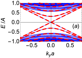
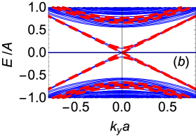
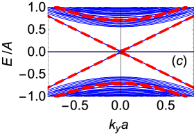
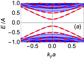
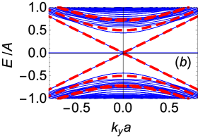
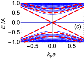
Using and , we determine the subband structure of Dirac electrons in the cases of and for , , and . To apply in determining the subband structure, we set , , , and and adopt the square lattice with the cross section shown in Fig. 3 with . Note that provides us with not only the subband structure of Dirac electrons but also that of bulk electrons. The factor for is obtained as and for the parameters given above. This implies that the penetration depth of 1D helical edge modes of QSHIs is on the order of one lattice constant. The subband structures in the case of are shown in Fig. 4. In this case, one nondegenerate subband remains gapless as is odd and the lowest gapped subband is doubly degenerate. The excitation gap of the latter is reduced with increasing as for , for , and for . As it is significantly reduced with increasing , we consider that the corresponding modes become pseudo-helical. The subband structures in the case of are shown in Fig. 5. In this case, no exactly gapless subband appears as is even and the lowest gapped subband is doubly degenerate. The corresponding excitation gap for is markedly reduced with increasing as for , and for , leading to the appearance of two pseudo-helical modes. In all the figures, the results obtained using and are almost identical as far as lower subbands are concerned.
Now, we consider the dimensionless conductance of the Dirac electron system on a side surface of weakly disordered WTIs in the cases of and . Following Ref. \citentakane1, we calculate at zero temperature by using the effective model given in Eq. (24) with the replacement of with . We randomly distribute -function-type impurities in a finite region of with and regard the semi-infinite regions of and as perfect leads. The impurity potential is given by with
| (29) |
where is the strength of the th impurity located at on the th chain. We assume that is uniformly distributed within the interval of . To obtain , we calculate the transmission matrix through the disordered region, in terms of which is determined as . For a given impurity configuration, is numerically obtained employing the method presented in Ref. \citentamura. To save computational time, we randomly choose points on the -axis within the sample region as and then put an impurity on every chain at each (). [16] The total number of impurities is . We compute the average dimensionless conductance by setting [35] and placing the Fermi level at and in the cases of and , respectively. In this setup, the gapless subband and the lowest gapped subband contribute to electron transport in the case of , while only the lowest gapped subband does so in the case of . The number of samples, , used in the average at each data point is more than . The relative uncertainty with is smaller than .
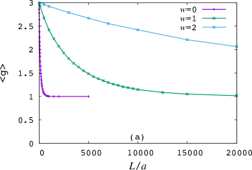
The average dimensionless conductance in the case of is shown in Fig. 6. In this case, decreases to unity with increasing owing to the presence of a PCC. We see that is enhanced with increasing width of steps. This should be attributed to the contribution of pseudo-helical modes induced by the step edges. With the increase in , their excitation gap decreases and therefore their backscattering is suppressed. This directly results in the enhancement of .
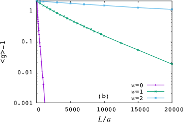
The average dimensionless conductance in the case of is shown in Fig. 7. In this case, decreases to zero with increasing reflecting the absence of a PCC. We see that is markedly enhanced with increasing . Particularly, with shows almost no decrease within the interval of shown in Fig. 7. This indicates that pseudo-helical modes become almost ideal in this case.
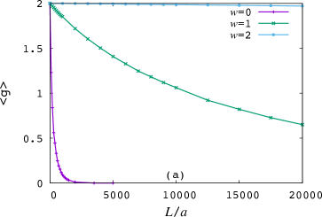
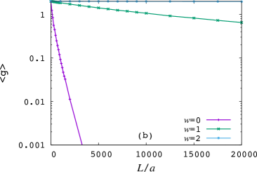
We observe from Figs. 6 and 7 that the enhancement of is stronger in the case of than in the case of . This indicates that an even number of layers placed in between pseudo-helical modes is very useful for enhancing the conductance of the system.
The above argument relies on for clearly observing the role of pseudo-helical modes. In other words, bulk states are ignored in calculating . However, their effect can be neglected as long as the Fermi level is much smaller than the energy gap of bulk states. [37]
In summary, we have shown that pseudo-helical modes with a nearly gapless linear dispersion can be created on a side surface of weak topological insulators by arranging straight step edges following the proposed prescriptions. We have also shown that such pseudo-helical modes significantly enhance the conductance of the system. Our proposal can be used as a useful building block in nanomaterials design. Its experimental application may not be easy at present but will be realized using the technique reported in Ref. \citenpauly. In realistic systems, the key parameter is the penetration depth of one-dimensional helical edge modes. We expect that the proposal becomes effective in realistic weak topological insulators when the width of step edges is comparable to, or larger than, the penetration depth.
Acknowledgment
This work was supported by JSPS KAKENHI Grant Number 15K05130.
References
- [1] L. Fu, C. L. Kane, and E. J. Mele, Phys. Rev. Lett. 98, 106803 (2007).
- [2] J. E. Moore and L. Balents, Phys. Rev. B 75, 121306 (2007).
- [3] R. Roy, Phys. Rev. B 79, 195322 (2009).
- [4] C. L. Kane and E. J. Mele, Phys. Rev. Lett. 95, 146802 (2005).
- [5] B. A. Bernevig and S.-C. Zhang, Phys. Rev. Lett. 96, 106802 (2006).
- [6] Y. Ran, Y. Zhang, and A. Vishwanath, Nat. Phys. 5, 298 (2009).
- [7] K.-I. Imura, Y. Takane, and A. Tanaka, Phys. Rev. B 84, 035443 (2011).
- [8] Z. Ringel, Y. E. Kraus, and A. Stern, Phys. Rev. B 86, 045102 (2012).
- [9] R. S. K. Mong, J. H. Bardarson, and J. E. Moore, Phys. Rev. Lett. 108, 076804 (2012).
- [10] C.-X. Liu, X.-L. Qi, and S.-C. Zhang, Physica E 44, 906 (2012).
- [11] K.-I. Imura, M. Okamoto, Y. Yoshimura, Y. Takane, and T. Ohtsuki, Phys. Rev. B 86, 245436 (2012).
- [12] Y. Yoshimura, A. Matsumoto, Y. Takane, and K.-I. Imura, Phys. Rev. B 88, 045408 (2013).
- [13] K. Kobayashi, T. Ohtsuki, and K.-I. Imura, Phys. Rev. Lett. 110, 236803 (2013).
- [14] T. Morimoto and A. Furusaki, Phys. Rev. B 89, 035117 (2014).
- [15] H. Obuse, S. Ryu, A. Furusaki, and C. Mudry, Phys. Rev. B 89, 155315 (2014).
- [16] Y. Takane, J. Phys. Soc. Jpn. 83, 103706 (2014).
- [17] T. Arita and Y. Takane, J. Phys. Soc. Jpn. 83, 124716 (2014).
- [18] Y. Takane, J. Phys. Soc. Jpn. 84, 084710 (2015).
- [19] A. Matsumoto, T. Arita, Y. Takane, Y. Yoshimura, and K.-I. Imura, Phys. Rev. B 92, 195424 (2015).
- [20] K. Kobayashi, Y. Yoshimura, K.-I. Imura, and T. Ohtsuki, Phys. Rev. B 92, 235407 (2015).
- [21] B.-H. Yan, L. Müchler, and C. Felser, Phys. Rev. Lett. 109, 116406 (2012).
- [22] B. Rasche, A. Isaeva, M. Ruck, S. Borisenko, V. Zabolotnyy, B. Buchner, K. Koepernik, C. Ortix, M. Richter, and J. van den Brink, Nat. Mater. 12, 422 (2013).
- [23] P. Tang, B. Yan, W. Cao, S.-C. Wu, C. Felser, and W. Duan, Phys. Rev. B 89, 041409 (2014).
- [24] G. Yang, J. Liu, L. Fu, W. Duan, and C. Liu, Phys. Rev. B 89, 085312 (2014).
- [25] C. Pauly, B. Rasche, K. Koepernik, M. Liebmann, M. Pratzer, M. Richter, J. Kellner, M. Eschbach, B. Kaufmann, L. Plucinski, C. M. Schneider, M. Ruck, J. van den Brink, and M. Morgenstern, Nat. Phys. 11, 338 (2015).
- [26] J.-J. Zhou, W. Feng, G.-B. Liu, Y. Yao, New J. Phys. 17, 015004 (2015).
- [27] T. Ando and H. Suzuura, J. Phys. Soc. Jpn. 71, 2753 (2002).
- [28] Y. Takane, J. Phys. Soc. Jpn. 73, 9 (2004).
- [29] Y. Takane, J. Phys. Soc. Jpn. 73, 1430 (2004).
- [30] Y. Takane, J. Phys. Soc. Jpn. 73, 2366 (2004).
- [31] T. Ando, J. Phys. Soc. Jpn. 75, 054701 (2006).
- [32] C.-X. Liu, X.-L. Qi, H. Zhang, X. Dai, Z. Fang, and S.-C. Zhang, Phys. Rev. B 82, 045122 (2010).
- [33] In Ref. \citenarita, is determined by a variational calculation. Equation (28) approximately reproduces the resulting in a simpler manner.
- [34] H. Tamura and T. Ando, Phys. Rev. B 44, 1792 (1991).
- [35] As should obey the scaling theory, [28, 36] we expect that a variation in results in only a renormalization of the mean free path. Hence, the dependence of is not qualitatively modified by such a variation.
- [36] A. M. S. Macêdo and J. T. Chalker, Phys. Rev. B 46, 14985 (1992).
- [37] Although the Fermi level assumed in our numerical calculations does not satisfy this condition, there is no essential difficulty in satisfying this in actual situations.