Atomic and electronic structure of the silicene phase on Ag(111): density-functional calculations
Abstract
Density-functional theory calculations are used to verify the atomic structure of the silicene phase grown on the Ag(111) surface. Recent experimental studies strongly suggested that the previous double-layer silicene model should be replaced with a Ag-mixed double-layer model resembling the top layers of the Ag/Si(111)-() surface. In our calculations, the Ag-mixed double-layer model is indeed energetically favored over the double-layer silicene model and well reproduces the reported scanning-tunneling microscopy and spectroscopy data. Especially, the structural origin of the experimental band structure is clarified as the top Ag-Si mixed layer, unlike the experimental interpretations as either a silicene layer or the Ag(111) substrate.
pacs:
68.43.Bc, 71.15.Mb, 81.07.VbI I. INTRODUCTION
Silicene, a monolayer of Si atoms arranged in a honeycomb lattice, has attracted great attention as a new Dirac-type electron system similar to graphene caha09 ; liuu11 ; ezaw12 ; ezaw13 ; pann14 . One practical way of preparing silicene is to grow it on metallic or half-metallic substrates such as ZrB2(0001) fleu12 , Ir(111) meng13 , and Ag(111) linn13 . Recent studies have been focused on the silicene fabricated on Ag(111) by thermal deposition of Si, exhibiting a variety of structural phases including 33 vogt12 ; majz13 ; liuu14 , chen12 ; chen13 ; chen13' , and linn12 ; john14 ; tcha14 with respect to the silicene unit cell, depending on the growth temperature and Si coverage.
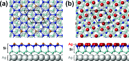
Particularly interesting is the silicene phase grown on Ag(111). This phase has been highlighted with exotic physical properties such as Dirac fermion charge carriers chen12 , temperature-induced structural transition chen13 , and superconductivity chen13' , but its atomic structure remains controversial. Chen and co-workers chen12 ; chen13 first proposed a single-layer silicene model, but it was questioned by scanning tunneling microscopy (STM) rest13 ; pado13 ; araf13 and atomic force microscopy (AFM) rest13 studies, in which the measured topographic heights imply a double-layer thickness of the silicene. A quantitative double-layer silicene model (see Fig. 1) was soon provided by Guo and Oshiyama by means of density functional theory (DFT) calculations guo14 .
This double-layer silicene model, however, was not supported by a low-energy electron diffraction (LEED) study of Shirai and co-workers shir14 : Their LEED data could not be explained by the double-layer silicene model, but instead were similar to that of the Ag/Si(111)-() surface. The Ag/Si(111)-() surface is well known for the Ag-induced surface reconstruction, referred to as the inequivalent-triangle model aiza99 , in which Ag atoms effectively replace the surface Si atoms with dangling bonds. Therefore, Shirai and co-workers shir14 suggested that the top part of the silicene double layer should be replaced with Ag atoms to resemble the adsorption structure of the Ag/Si(111)-() surface, as schematically shown in Fig. 1(b). Interestingly, Mannix and co-workers mann14 also independently reached the same mixed double-layer (MDL) picture from the similar STM images between the silicene phase on Ag(111) and the Ag/Si(111)-() surface. The energetical, microscopic and spectroscopic tests of the experimental MDL model, however, is yet to be done.
In this paper, we use DFT calculations to examine the MDL model for the silicene phase grown on Ag(111). The MDL model is found to form a stable adsorption structure on the Ag(111) substrate, which is energetically favored over the earlier double-layer silicene model. The MDL model is also sound both microscopically and spectroscopically: Its electronic structure accounts well for the measured STM images and band structures.
II II. METHOD
We perform DFT calculations using the Vienna simulation package kres96 within the Perdew-Burke-Ernzerhof generalized gradient approximation perd96 and the projector augmented wave method bloc94 ; kres99 . The Ag(111) surface is modeled by a periodic slab geometry with five atomic layers and a vacuum spacing of about 19 Å. Si and Ag atoms are incorporated on the top of the Ag(111)-(44) slab unit cell, a supercell commensurating with the silicene-() lattice guo15 . The calculated value 2.938 Å is used as the bulk Ag-Ag bond length, which is in good agreement with the experimental value 2.892 Å kitt05 . We expand the electronic wave functions in a plane-wave basis with an energy cutoff of 250 eV. A (661) -point mesh is used for the (44) Brillouin-zone integrations. All atoms but the bottom two Ag layers are relaxed until the residual force components are within 0.02 eV/Å. The used slab and vacuum thickness, plane-wave energy, and -point mesh were found to produce sufficiently converged results for the MDL model: the formation energy and the interatomic distances converge well within 0.05 eV and 0.02 Å, respectively. We compare the energetics between different models by estimating the relative formation energy, defined by , where () is the total energy of a particular model (a reference model), is the number difference of the specified atoms relative to the reference model, and is the calculated bulk chemical potential for the specified atom.
III III. RESULTS
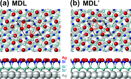
Figure 2 shows two energetically-degenerated MDL structures under consideration, which were well established in the Ag/Si(111)-() system aiza99 . The MDL structure is characterized by two inequivalent Ag triangles, and the MDL′ structure is distinguishable with the mirror-symmetric conversion of the two Ag triangles. The MDL and MDL′ structures can be transformed to each other by relatively small displacements of the top Ag (0.5 Å) and Si (0.3 Å) atoms. We calculated the corresponding energy barrier by using the nudged elastic-band method jons98 that allows an effective search for the lowest-energy path for a multi-atomic structural transition. The result is as low as 66 meV per silicene unit cell. This low energy barrier and the resulting thermal fluctuations will be discussed below in accounting for the STM feature that the silicene phase on Ag(111) appears differently at above 40 K from two distinct mirror-symmetric images at lower temperatures chen13 .
| 3.01 | 2.54 | 0.69 | 2.32 | 0.80 | 2.26 |
Table I summarizes the structural details of the MDL model shown in Fig. 2(a). The Ag-Ag (3.01 Å) and Si-Si (2.54 Å) bond lengths and the Ag-Si (0.69 Å) and Si-Si′ (2.32 Å) layer spacings compare well with those (3.00, 2.58, 0.72, and 2.29 Å, respectively) of the inequivalent-triangle Ag/Si(111)-() surface aiza99 . The mixed double layer is separated by 2.26 Å from the Ag(111) substrate. The resulting Si-Ag bond lengths of about 2.56 Å implies a covalent bonding between Si and Ag atoms in view that the covalent radii of Si and Ag are 1.11 Å and 1.45 Å cord08 , respectively, as was already argued by Guo and Oshiyama in their DFT study of the double-layer silicene model guo14 .
The MDL model is more stable in energy than the double-layer silicene model of Guo and Oshiyama guo14 . Its lower formation energy by 1.02 eV per silicene unit cell is possibly attributed to the removal of Si dangling bonds by Ag substitution for the top-layer Si atoms. On the other hand, the MDL model has 0.66 eV higher formation energy than the well-established 33 single-layer silicene phase vogt12 , supporting the experimental finding that, as increasing the Si coverage, the silicene phase appears after covered with the 33 phase vogt14 .
The MDL model accounts well for the apparent height difference in STM and AFM topographs between the and the 33 silicene phases on Ag(111) rest13 ; pado13 ; araf13 . In our calculations, the topmost layer of the present MDL model is 3.14 Å higher than that of the 33 single-layer silicene structure vogt12 , which compares well with the AFM measurement of 3.0 Å rest13 and the STM measurement of 2.2 Å pado13 ; araf13 . Somewhat smaller STM result may possibly reflect different surface electronic structures of the two phases.
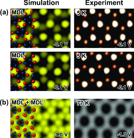
Figure 3(a) shows the simulated STM images of the two mirror-symmetric MDL structures shown in Fig. 2. Both images feature two superposed hexagonal arrays: one with bright spots and the other with weaker spots, representing the centers of small and large Ag triangles, respectively. Here, the top-layer Si triangles appear dark in both images. It is experimentally known that the silicene phase shows two mirror-symmetric configurations separated by narrow domain boundaries at low temperatures below 40 K chen13 . The STM images measured at 5 K, representing two different domains, indeed compare well with our simulations. At elevated temperatures, however, thermal fluctuations may take place between the two mirror-symmetric (MDL and MDL′) structures. Figure 3(b) shows the superposition of the two mirror-symmetric images, appearing as a prominent honeycomb array, which compares well with the STM image taken at 77 K chen13 . The experimental honeycomb image appears more symmetric than the simulation possibly due to the rounding effect of thermal fluctuations.”
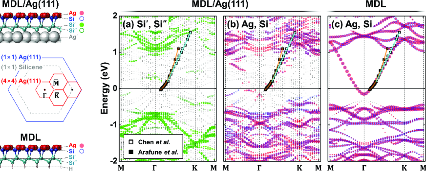
Figure 4 shows the calculated band structure of the MDL model in comparison with scanning tunneling spectroscopy (STS) measurements chen13 ; araf13 . While Chen and co-workers chen13 reported an almost linear band (denoted by open squares) and attributed its origin to the silicene layer, Arafune and co-workers araf13 claimed that their STS band (denoted by filled squares) must be described by a parabolic function and originates from the Ag(111) substrate. In our layer-resolved band analysis, however, the experimental bands could be related to neither the Si′ and Si′′ layers of the mixed double layer nor the Ag(111) substrate, as seen in Fig. 4(a). They instead can be related to the Ag and Si mixed layer although the calculated band character appears rather weak possibly due to the resonance mixing with the broadly-spread bulk states steming from the Ag(111) substrate. In order to clarify the band picture of the Ag and Si mixed layer, we examined the band structure of the isolated MDL structure, the bottom of which is now terminated by H atoms instead of the Ag(111) substrate. Here, as shown in Fig. 4(c), the Ag and Si mixed layer produces a prominent surface band near the Fermi level, exhibiting a nearly parabolic shape. A parabolic fitting to the bottom part (below 0.2 eV) results in an effective mass of 0.11 ( is the mass of free electron), comparable to the experimental value 0.14 reported by Arafune and co-workers araf13 . In the range of 0.2–1.0 eV, the band shows an almost linear dispersion, and the calculated velocity of 0.84106 m/s also compares well with the experimental value 0.97106 m/s reported by Chen and co-workers chen13 . Therefore, the present MDL model not only reproduces the experimental band structure but also corrects the previous misinterpretations of the band origin: It is not from either a silicene layer or the Ag(111) substrate, but from the top Ag-Si mixed layer.
In light of the present confirmation of the MDL model, it is noticeable that a recent STM study refuted the possibility of Ag segregation to the top silicene layer. In their STM study of multi-layer silicene films grown on Ag(111) chen15 , Chen and co-workers applied bias pulses to the tip on the surface, thereby removing a part of the surface layers beneath the tip at liquid nitrogen temperature. Interestingly, the underneath exposed layer (supposed to be a pure silicene layer) also showed a similar STM image to the top layer, and they inferred from the similar STM images that the top layer is also a pure silicene layer. It should be mentioned, however, that the similar STM images do not necessarily guarantee the identical atomic structures. In fact, the double-layer silicene model by Guo and Oshiyama guo14 and the present MDL model are equally compatible with the experimental honeycomb image chen13 . So, the top mixed layer and deeper pure silicene layers could also be compatible with the reported STM observations of Chen and co-workers chen15 . Only the comparison of the STM images is not yet sufficient for a definite chemical and structural assignment.
IV IV. SUMMARY
The present DFT calculations confirmed the experimentally-proposed mixed double-layer model for the silicene phase grown on Ag(111) by demonstrating that it is energetically sound and well reproduces the reported STM images and STS band structures.
V ACKNOWLEDGMENTS
This work was supported by the National Research Foundation of Korea (Grant No. 2011-0008907).
References
- (1) S. Cahangirov, M. Topsakal, E. Aktürk, H. Şahin, and S. Ciraci, Two- and one-dimensional honeycomb structures of silicon and germanium, Phys. Rev. Lett. 102, 236804 (2009).
- (2) C.-C. Liu, W. Feng, and Y. Yao, Quantum spin hall effect in silicene and two-dimensional germanium, Phys. Rev. Lett. 107, 076802 (2011).
- (3) M. Ezawa, Valley-polarized metals and quantum anomalous hall effect in silicene, Phys. Rev. Lett. 109, 055502 (2012).
- (4) M. Ezawa, Photoinduced topological phase transition and a single dirac-cone state in silicene, Phys. Rev. Lett. 110, 026603 (2013).
- (5) H. Pan, Z. Li, C.-C. Liu, G. Zhu, Z. Qiao, and Y. Yao, Valley-polarized quantum anomalous hall effect in silicene, Phys. Rev. Lett. 112, 106802 (2014).
- (6) A. Fleurence, R. Friedlein, T. Ozaki, H. Kawai, Y. Wang, and Y. Yamada-Takamura, Experimental evidence for epitaxial silicene on diboride thin films, Phys. Rev. Lett. 108, 245501 (2012).
- (7) L. Meng, Y. Wang, L. Zhang, S. Du, R. Wu, L. Li, Y. Zhang, G. Li, H. Zhou, W. A. Hofer, and H.-J. Gao, Buckled silicene formation on Ir(111), Nano Lett. 13, 685 (2013).
- (8) C.-L. Lin, R. Arafune, K. Kawahara, M. Kanno, N. Tsukahara, E. Minamitani, Y. Kim, M. Kawai, and N. Takagi, Substrate-induced symmetry breaking in silicene, Phys. Rev. Lett. 110, 076801 (2013).
- (9) P. Vogt, P. De Padova, C. Quaresima, J. Avila, E. Frantzeskakis, M. C. Asensio, A. Resta, B. Ealet, and G. Le Lay, Silicene: compelling experimental evidence for graphenelike two-dimensional silicon, Phys. Rev. Lett. 108, 155501 (2012).
- (10) Z. Majzik, M. Rachid Tchalala, M. vec, P. Hapala, H. Enriquez, A. Kara, A. J. Mayne, G. Dujardin, P. Jelíınek, and H. Oughaddou, Combined AFM and STM measurements of a silicene sheet grown on the Ag(111) surface, J. Phys.: Condens. Matter. 25, 225301 (2013).
- (11) Z.-L. Liu, M.-X. Wang, J.-P. Xu, J.-F. Ge, G. L. Lay, P. Vogt, D. Qian, C.-L. Gao, C. Liu, and J.-F. Jia, Various atomic structures of monolayer silicene fabricated on Ag(111), New J. Phys. 16, 075006 (2014).
- (12) L. Chen, C.-C. Liu, B. Feng, X. He, P. Cheng, Z. Ding, S. Meng, Y. Yao, and K.Wu, Evidence for dirac fermions in a honeycomb lattice based on silicon, Phys. Rev. Lett. 109, 056804 (2012).
- (13) L. Chen, H. Li, B. Feng, Z. Ding, J. Qiu, P. Cheng, K. Wu, and S. Meng, Spontaneous symmetry breaking and dynamic phase transition in monolayer silicene, Phys. Rev. Lett. 110, 085504 (2013).
- (14) L. Chen, B. Feng, and K. Wu, Observation of a possible superconducting gap in silicene on Ag(111) surface surface, Appl. Phys. Lett. 102, 081602 (2013).
- (15) C.-L. Lin, R. Arafune, K. Kawahara, N. Tsukahara, E. Minamitani, Y. Kim, N. Takagi, and M. Kawai, Structure of silicene grown on Ag(111), Appl. Phys. Express. 5, 045802 (2012).
- (16) N. W. Johnson, P. Vogt, A. Resta, P. D. Padova, I. Perez, D. Muir, E. Z. Kurmaev, G. L. Lay, and A. Moewes, The metallic nature of epitaxial silicene monolayers on Ag(111), Adv. Funct. Mattert. 24, 5253 (2014).
- (17) M. R. Tchalala, H. Enriquez, H. Yildirim, A. Kara, A. J. Mayne, G. Dujardin, M. A. Ali, and H. Oughaddou, Atomic and electronic structures of the ()R13.9∘ of silicene sheet on Ag(111), Appl. Surf. Sci. 303, 61 (2014).
- (18) R. Arafune, C.-L. Lin, K. Kawahara, N. Tsukahara, E. Minamitani, Y. Kim, N. Takagi, and M. Kawai, Structural transition of silicene on Ag(111), Surf. Sci. 608, 297 (2013).
- (19) P. De Padova, P. Vogt, A. Resta, J. Avila, I. Razado-Colambo, C. Quaresima, C. Ottaviani, B. Olivieri, T. Bruhn, T. Hirahara, T. Shirai, S. Hasegawa, M. C. Asensio, and G. Le Lay, Evidence of Dirac fermions in multilayer silicene, Appl. Phys. Lett. 102, 163106 (2013).
- (20) A. Resta, T. Leoni, C. Barth, A. Ranguis, C. Becker, T. Bruhn, P. Vogt, and G. Le Lay, Atomic structures of silicene layers grown on Ag(111): scanning tunneling microscopy and noncontact atomic force microscopy observations, Sci. Rep. 3, 2399 (2013).
- (21) Z. X. Guo and A. Oshiyama, Structural tristability and deep Dirac states in bilayer silicene on Ag(111) surfaces, Phys. Rev. B 89, 155418 (2014).
- (22) T. Shirai, T. Shirasawa, T. Hirahara, N. Fukui, T. Takahashi, and S. Hasegawa, Structure determination of multilayer silicene grown on Ag(111) films by electron diffraction: evidence for Ag segregation at the surface, Phys. Rev. B 89, 241403 (2014).
- (23) H. Aizawa, M. Tsukada, N. Sato, S. Hasegawa, Asymmetric structure of the Si(111)--Ag surface, Surf. Sci. Lett. 429, L509 (1999).
- (24) A. J. Mannix, B. Kiraly, B. L. Fisher, M. C. Hersam, and N. P. Guisinger, Silicon growth at the two-dimensional limit on Ag(111), ACS Nano 8, 7538 (2014).
- (25) G. Kresse and J. Furthmüller, Efficient iterative schemes for total-energy calculations using a plane-wave basis set, Phys. Rev. B 54, 11169 (1996).
- (26) J. P. Perdew, K. Burke, and M. Ernzerhof, Generalized gradient approximation made simple, Phys. Rev. Lett. 77, 3865 (1996).
- (27) P. E. Blöchl, Projector augmented-wave method, Phys. Rev. B 50, 17953 (1994).
- (28) G. Kresse and D. Joubert, From ultrasoft pseudopotentials to the projector augmented-wave method, Phys. Rev. B 59, 1758 (1999).
- (29) Z. X. Guo and A. Oshiyama, Crossover between silicene and ultra-thin Si atomic layers on Ag, New J. Phys. 17, 045028 (2015).
- (30) C. Kittel, Introduction to Solid State Physics, 8th ed. (Wiley, New York, 2005).
- (31) H. Jónsson, G. Mills, and K. W. Jacobsen, in Classical and Quantum Dynamics in Condensed Phase Simulations, edited by B. J. Berne, G. Ciccotti, and D. F. Coker (World Scientific, Singapore, 1998).
- (32) B. Cordero, V. Gómez, A. E. Platero-Prats, M. Revés, J. Echeverría, E. Cremades, F. Barragán, and S. Alvarez, Covalent radii revisited, Dalton Trans. 21, 2832 (2008).
- (33) P. Vogt, P. Capiod, M. Berthe, A. Resta, P. De Padova, T. Bruhn, G. Le Lay, and B. Grandidier, Synthesis and electrical conductivity of multilayer silicene, Appl. Phys. Lett. 104, 021602 (2014).
- (34) J. Chen, Y. Du, Z. Li, W. Li, B. Feng, J. Qiu, P. Cheng, S. X. Dou, L. Chen, and K. Wu, Delocalized Surface State in Epitaxial Si(111) Film with Spontaneous Superstructure, Sci. Rep. 5, 13590 (2015).