Contact resistances in trigate and FinFET devices in a Non-Equilibrium Green’s Functions approach
Abstract
We compute the contact resistances in trigate and FinFET devices with widths and heights in the 4 to 24 nm range using a Non-Equilibrium Green’s Functions approach. Electron-phonon, surface roughness and Coulomb scattering are taken into account. We show that represents a significant part of the total resistance of devices with sub-30 nm gate lengths. The analysis of the quasi-Fermi level profile reveals that the spacers between the heavily doped source/drain and the gate are major contributors to the contact resistance. The conductance is indeed limited by the poor electrostatic control over the carrier density under the spacers. We then disentangle the ballistic and diffusive components of , and analyze the impact of different design parameters (cross section and doping profile in the contacts) on the electrical performances of the devices. The contact resistance and variability rapidly increase when the cross sectional area of the channel goes below nm2. We also highlight the role of the charges trapped at the interface between silicon and the spacer material.
I Introduction
The electrical performances of field-effect transistors are increasingly limited by the contact resistances as the gate length decreases.ITR ; Kuhn (2012) At low drain bias , the “apparent” contact resistance can be defined as the linear extrapolation to zero gate length of the total resistance of the device. It embeds, therefore, all contributions that are independent of , namely: i) the resistance of the metal-semiconductor contact, ii) the resistance of the highly doped source/drain and of the lowly doped spacers between the contacts and the gate, and iii) the so-called “ballistic” resistance of the device (residual resistance in the absence of scattering mechanisms). Although the latter can be intrinsic to the channel, it is usually considered part of the contact resistance as it is independent on the gate length.
There has been a lot of theoretical and experimental works aimed at understanding and improving the transport through the channel of the transistor. At low field, the resistance of the channel can be characterized by the carrier mobility , which has been extensively measured and calculated in a variety of silicon structures (bulk,Jacoboni and Reggiani (1983) filmsGamiz and Fischetti (2001); Esseni et al. (2003); Uchida and Takagi (2003); Casse et al. (2006); Jin, Fischetti, and Tang (2007); Toniutti et al. (2012); Niquet et al. (2014); Nguyen et al. (2014); Niquet et al. (2015) and wiresKotlyar et al. (2004); Jin, Fischetti, and wei Tang (2007); Ramayya et al. (2008); Poli et al. (2008); Poli, Pala, and Poiroux (2009); Persson et al. (2010); Neophytou and Kosina (2011); Lee et al. (2011); Kim et al. (2011); Aldegunde, Martinez, and Asenov (2011); Luisier (2011); Akarvardar et al. (2012); Nguyen et al. (2013); Coquand et al. (2013a, b)). There is much less literature on the contact resistances,Kim, Park, and Woo (2002a, b); Dixit et al. (2005); Magnone et al. (2008); Tekleab, Samavedam, and Zeitzoff (2009); Parada et al. (2011); Park et al. (2013); Sohn et al. (2013); An et al. (2014); Pereira and Giacomini (2015); Yoon et al. (2015); Berrada et al. (2015) even though they have become a major bottleneck for device performances. Most models for the contact resistances are based on drift-diffusion equations needing carrier mobilities as input, which might not be well characterized in the very inhomogeneous source/drain extensions.
In this work, we compute the contact resistances of -type, oriented nanowire transistorsColinge (2004) with widths and heights in the 4 to 24 nm range. We use a Non-Equilibrium Green’s Functions (NEGF) approach, which explicitly accounts for confinement and scattering by phonons, surface roughness, and dopants in the inhomogeneous source and drain.Anantram, Lundstrom, and Nikonov (2008) We consider square () and rectangular () trigate devices as well as FinFET () devices with realistic, bulk-like source and drain contacts. We focus on components ii) and iii) of the contact resistance (source/drain extensions and ballistic resistances), and show that they indeed represent a significant fraction of the total resistance of these devices. The methodology, based on the data extrapolation, is a numerical implementation of the transmission line approachSho ; Niquet et al. (2014) (section II). It can be supplemented with a quasi-Fermi level analysis (section III), which highlights where the potential drops are located in the device, and helps to bridge NEGF with Technology Computer Aided Design (TCAD) tools based on drift-diffusion models. The quasi-Fermi level profile shows, in particular, that the contact resistance is dominated by the lowly doped spacers between the source/drain and the channel. We then disentangle the ballistic contribution from the scattering by phonons, surface roughness and impurities (section IV). Simple models for the different terms confirm that the contact conductance is most often limited by the (poor) electrostatic control over the carrier density in the spacers. We next discuss the impact of some design parameters (channel cross section and doping profile) on the carrier mobility in the channel, contact resistance and device variability (section V). We also investigate the effect of charges trapped at the interface between the silicon wire and the spacer material (Si3N4). We finally provide experimental support for the main conclusions of this work (section VI).
II Methodology and devices
In this section, we discuss the devices, the NEGF approach, the numerical transmission line method for the contact resistance, and a specific example.
II.1 Devices
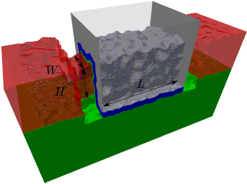
A typical device is represented in Fig. 1. The channel is a oriented rectangular nanowire with width and height , etched in a Silicon-On-Insulator (SOI) layer.Coquand et al. (2013a, b) It is lying on a 25 nm thick buried oxide (BOX) and a -doped Si substrate (donor concentration cm-3). The gate stack covers the top and side facets of the nanowire. It is made of a 0.8 nm thick layer of SiO2 (dielectric constant ) and a 2.2 nm thick layer of HfO2 (). The source and drain are modeled as films with thickness nm. Periodic boundary conditions are, therefore, applied along , on both potential and wave functions.Not The width of the unit cell is nm. The length of the source and drain films included in the simulation domain is nm. The source and drain are separated from the gate by Si3N4 spacers with length nm ().
Surface roughness (SR) and charge disorders are explicitly included in the geometries. For SR, we use a Gaussian auto-correlation function modelGoodnick et al. (1985) with different correlation lengths and rms on different facets: nm and nm on the bottom interface with the BOX, nm and nm on the top facet, and nm, nm on the side facets. We also include Remote Coulomb Scattering (RCS) in the gate stack as a distribution of positive charges at the SiO2/HfO2 interface with density cm-2. The SR parameters for the top and bottom interfaces are chosen to reproduce the experimental mobility in planar FDSOI devices (along the lines of Ref. Nguyen et al., 2014). The SR parameters of the side facets as well as are chosen to reproduce the experimental mobility in nm trigate devices (see section III). The sidewalls appear rougher than the top and bottom interfaces because they are etched in the SOI film.
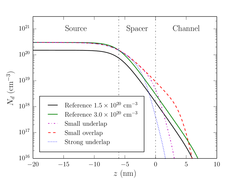
The source, drain and spacers are -doped with point charges as models for ionized donor impurities. These point charges are randomly scattered using the doping profiles shown in Fig. 2 as target distribution functions. The “Reference” profiles have cm-3 or cm-3 in the contacts, and a single decay length nm/decade under the spacers and channel. The other profiles will be discussed in detail in section V.2. Near the edges of the simulation box the point charge distributions are mixed with the target continuous background charge distributions in order to smooth the variations of the potential at the boundaries where the contact self-energiesAnantram, Lundstrom, and Nikonov (2008) are plugged in.not
II.2 The NEGF approach
The current is computed in a self-consistent NEGF framework,Anantram, Lundstrom, and Nikonov (2008); Stefanucci and van Leeuwen (2013) within the effective mass approximation (EMA).Bastard (1988) The NEGF equations are solved on a finite differences grid (with 2 Å step), in a fully coupled mode space approach (160 to 352 modes depending on the cross section). Electron-phonon scattering is described by an acoustic deformation potential eV,Esseni et al. (2003) and by the three and three inter-valley processes of Ref. Jacoboni and Reggiani, 1983. Technical details about the electron-phonon self-energies and solution of the NEGF equations can be found in the Appendix of Ref. Niquet et al., 2014. The -doped substrate is biased at back-gate voltage V and is treated semi-classically.Sze and Kwok (2006)
Electron-electron interactions are treated in a self-consistent “Schrödinger-Poisson” approximation, i.e. the carriers are moving in the potential created by the average density of conduction band electrons in silicon. The effects of valence band electrons in silicon and other materials are accounted for by the dielectric constants introduced in Poisson’s equation. This approximation neglects Coulomb correlations that might, however, become important in nanoscale devices.Fischetti et al. (2009) As a step further, we have introduced (in a few test cases) a -like self-energy accounting for the long-range correlations brought by the dielectric mismatch between the different materials, supplemented with a local density approximation for the short-range exchange-correlation effects.Jin, Fischetti, and Tang (2007); Li, Bescond, and Lannoo (2009); Niquet et al. (2015); Lavieville et al. (2015) This has a moderate impact on the contact resistances ( increase). Since the calculation of this -like self-energy is very demanding, these corrections have been neglected in the following.
One of the main advantages of NEGF is that all structural scattering mechanisms (SR, impurity and RCS scattering) are treated explicitly. There is no need for models for the interactions with these disorders. As a matter of fact, such models are still missing under the spacers, which are very inhomogeneous but critical regions on the resistive path (see sections III and IV). Also, at variance with most previous NEGF calculations,Poli et al. (2008); Poli, Pala, and Poiroux (2009); Luisier (2011); Aldegunde, Martinez, and Asenov (2011); Nguyen et al. (2013); Seoane et al. (2009); Martinez et al. (2011); Berrada et al. (2015) the source and drain contacts are wide enough with respect to the channel to act as bulk reservoirs (with a 3D-like density of states). This is essential for a quantitative description of the contact resistances. The convergence with respect to , and has, in particular, been carefully checked.
II.3 Methodology
At low drain bias , the total resistance of the device is expected to increase linearly with gate length :Datta, Assad, and Lundstrom (1998)
| (1) |
where is the drain current, is the diffusive resistance of the source, is the diffusive resistance of the drain, is the carrier mobility and the carrier density per unit length in the channel, and is the ballistic resistance of the device (residual resistance in the absence of scattering mechanisms).Datta, Assad, and Lundstrom (1998); Shur (2002) At zero temperature, the ballistic conductance of a homogeneous conductor, , is limited by the number of 1D sub-bands carrying current. At room temperature, reads, assuming Maxwell-Boltzmann statistics and a single transport mass for all sub-bands:Datta, Assad, and Lundstrom (1998); Nguyen et al. (2013)
| (2) |
It is, therefore, proportional to the carrier density in the conductor – we will come back to that point in section IV.
The “apparent” contact resistance can hence be extracted from the linear extrapolation of down to (an approach known as the transmission line methodSho ). For that purpose, we prepare a series of devices with lengths nm and nm (and up to nm), sharing the same contacts (source/drain/spacers geometry and dopant distributions). In order to limit the noise on the data that might arise from different disorders at different ’s, we repeat the 30 nm long sample of surface roughness and RCS charges along the and nm long channels.Niquet et al. (2014) We can extract that way the resistance of the chosen contact geometry and dopant distribution very accurately. We then average the contact resistance over 3 to 8 surface roughness profiles and dopant distributions in order to assess local variability.
In order to ease the comparison between devices with different cross sections, the carrier densities and the resistances are normalized to the total effective width of the channel . The drain bias is mV, and the threshold voltage is extracted from the function (where is the transconductance and the gate bias).Ghibaudo (1988) There are no significant short-channel effects (in particular, no roll-off) in any of the investigated devices.
II.4 Example: The nm trigate
In this paragraph, we illustrate the above methodology on a specific example: The nm trigate device with the “Reference cm-3” doping profile of Fig. 2.
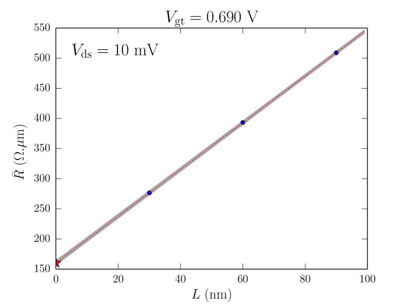
The total resistance of a series of devices is plotted as a function of the channel length in Fig. 3, at gate overdrive V. As expected, the resistance scales linearly with length in the inversion regime. The contact resistance (red star on Fig. 3) and the channel mobility can therefore be extracted from these data. is plotted as a function of the gate overdrive and carrier density in the channel in Fig. 4. is defined as the average carrier density in the central, 30 nm long segment of the 60 nm long channel. follows an approximate (or ) trend (with close to 1). As the conductivity is proportional to the carrier density in the simplest Drude model, this trend suggests that the contact resistance is dominated by the near channel (spacers) region.Rideau et al. (2014) This will be confirmed by a quasi-Fermi level analysis in the next section.
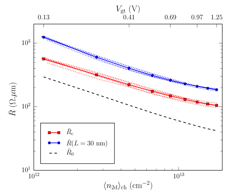
Data for five devices with different disorders are represented in Fig. 4. The local variability due to fluctuations in surface roughness and dopant distributions remains weak in nm devices. is compared to the total resistance of the 30 nm long devices, and to the the resistance of the corresponding “ballistic” device (neither phonons, nor SR and RCS, with a continuous background dopant distribution in the contacts). The contact resistance is around half the total resistance in a 30 nm long device – it would hence be as large as two-thirds the total resistance in a nm long channel. It is, moreover, much larger than the ballistic resistance (especially in the strong inversion regime), which is a component and lower bound of . The optimization of the source/drain/spacers region is, therefore, at least as important as the design of the channel in these transistors.
III A quasi-Fermi level analysis of the resistive path
The above conclusions can be further supported by a quasi-Fermi level analysis, which highlights where the potential drops in the system. We first define the quasi-Fermi level in the NEGF framework, then discuss limiting cases (ballistic and diffusive conductors), and finally make a detailed analysis on the trigate device of paragraph II.4.
III.1 Definition
Drift-diffusion modelsSze and Kwok (2006) assume that the carriers are in local equilibrium with a quasi-Fermi level . The current density in the device is then proportional to the gradient of :
| (3) |
In the NEGF framework, the carriers can be driven far out-of-equilibrium, so that the quasi-Fermi level is, in general, ill-defined. The distribution of electrons can instead be characterized by the local distribution function:
| (4) |
where is the density of occupied states (with the lesser Green’s function), and is the total density of states (with the retarded Green’s function).Anantram, Lundstrom, and Nikonov (2008) Yet a detailed analysis shows that remains close to a Fermi function at low bias. In that limit, we can define the quasi-Fermi level as the chemical potential that reproduces the NEGF carrier density assuming local Fermi-Dirac statistics:
| (5) |
where is the reduced Fermi function.
The quasi-Fermi level analysis is an efficient way to bridge NEGF with the drift-diffusion models widely used in industrial TCAD tools. For practical purposes, we define a one-dimensional quasi-Fermi level in the device from the relation:
| (6) |
where and are the NEGF carrier density and density of states per unit length, which are the integrals of and in the cross section at .
III.2 Limiting cases: Ballistic and diffusive conductors
In this paragraph, we address two limiting cases: the ballistic and diffusive conductors. We discuss how the quasi-Fermi level drops in these conductors, in order to provide guidelines for the analysis of trigate and FinFET devices.
Although the carrier distribution in a ballistic conductor is definitely not a Fermi-Dirac distribution,Rhew, Ren, and Lundstrom (2002) the solution of Eq. (6) remains unambiguously defined. Let us consider a ballistic transistor in the ON state, at low and low temperature. The potential in such a transistor can be modeled in a first approximation as a square barrier. Carriers with positive group velocities (labeled as wave vectors for simplicity) are injected from the source and are in equilibrium with the chemical potential . Carriers with negative group velocities () are injected from the drain and are in equilibrium with the chemical potential . If the carrier density is much lower in the channel than in the source and drain (which is usually the case), most of the electrons are backscattered by the barrier, and only a small fraction flows in the channel. The quasi-Fermi level hence tends to in the source, and to in the drain. In the channel, there is a population of carriers with positive group velocities flowing from the source and in equilibrium with , and a population of carriers with negative group velocities flowing from the drain and in equilibrium with . Hence, all states are filled below , while only the states are occupied between and . If the density of states is approximately constant in the range, the quasi-Fermi level in the channel must be in order to match the carrier density with a Fermi-Dirac distribution.
This argument shows that the quasi-Fermi level essentially drops at both ends of the channel in a ballistic device.Büttiker et al. (1985); Datta (1995) Ballistic device simulations confirm that this is indeed the case. The width of the drop on each end of the channel depends, in particular, on the shape of the barrier and on the temperature. The drop is typically faster in the strong than in the weak inversion regime, where the quasi-Fermi level can show significant variations over the whole channel in short devices.
In a diffusive conductor on the other hand, the current must be sustained by a finite electric field. The quasi-Fermi level shall show the same variations as the potential if the density is approximately constant, i.e. it shall drop linearly in the channel at low bias.
As a concluding remark, we would like to emphasize that the above analysis only applies at low bias, and might break down at large in both ballisticRhew, Ren, and Lundstrom (2002) and diffusive cases.
III.3 Application to the nm trigate
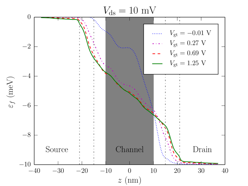
The quasi-Fermi level computed in the same device as in paragraph II.4 is plotted in Fig. 5 at different gate overdrives (drain bias mV).
As expected from the above discussion, the quasi-Fermi level tends to zero in the source (reference chemical potential ), and to in the drain. Moreover, the quasi-Fermi level is almost constant in the source and drain, and drops under the spacers and in the channel. These regions are, therefore, the most resistive parts of the device. The resistance of the heavily doped, bulk source and drain is negligible because the density of carriers and cross sectional area are much larger there than in the channel, even though the mobility is expected to be very low in the contacts ( cm2/V/s).Jacoboni et al. (1977)
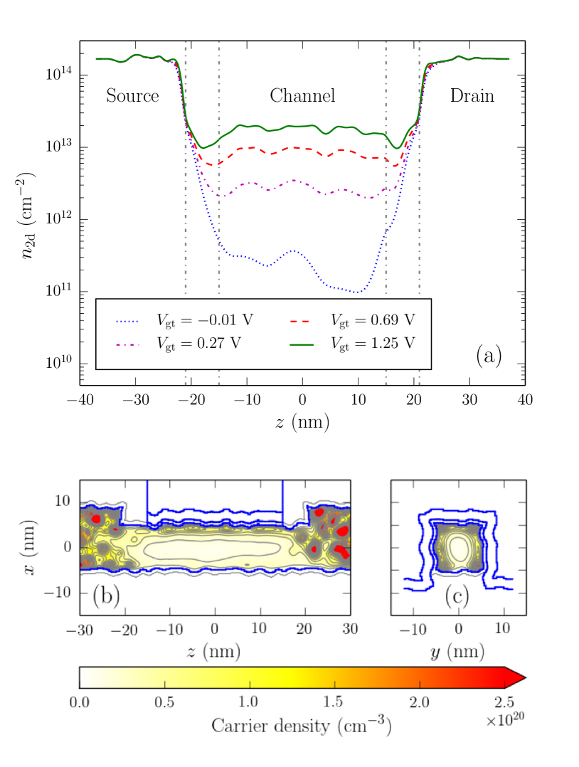
The quasi-Fermi level profile is, nonetheless, strongly dependent on the gate bias. Near or under the threshold, the transport is strongly limited by the bell-shaped barrier under the gate. The density is, moreover, very inhomogeneous in the channel (see Fig. 6). The quasi-Fermi level drops unevenly in the channel, and no clear distinction can be made between a ballistic and a diffusive (scattering-limited) component.
The picture is clearer at moderate to strong inversion. The carrier density is much more homogeneous under the gate. The quasi-Fermi level drops quasi-linearly in the channel, and exhibits two steps under the spacers. We can conjecture from paragraph III.2 that i) the transport in the channel is diffusive (the carrier mobility shall hence be proportional to slope of the quasi-Fermi level under the gate) ; ii) the drop of the quasi-Fermi level under the spacers is proportional to the contact resistance (including the ballistic component ).
To support these conclusions, we have recomputed the channel mobility and contact resistance from the relations:
| (7a) | |||
| (7b) | |||
where is the slope of the quasi-Fermi level extracted from a linear regression in the inner nm range of the 30 nm long channel.
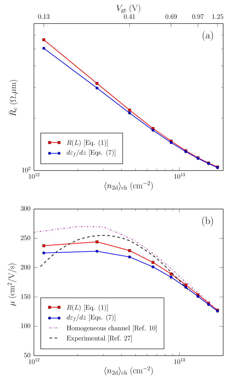
The mobility and contact resistance obtained that way are plotted in Fig. 7. They are in very good agreement with those extracted with the transmission line methodology of paragraph II.3 in the strong inversion regime, where the quasi-Fermi level drops quasi-linearly under the gate. The contact resistance is, therefore, indeed dominated by the spacers.Rideau et al. (2014) The mobility also compares well with that extracted from the data on “homogeneous” nanowire channels without spacers and bulk source/drain contacts (the gate then runs across the whole simulation box – see Ref. Niquet et al., 2014). The differences at low are due to the source/channel and channel/drain junctions, whose finite depletion widths result in significant variations of the carrier density near both ends of the channel (see Fig. 6). As a matter of fact, homogeneous nanowire channels without such junctions are better suited to the calculation of the long-channel mobility at low carrier density.Niquet et al. (2014) The calculated mobilities are close to the experimental data of Ref. Coquand et al., 2013b whatever the methodology.
The analysis of the quasi-Fermi level provides an alternative to the methodology of paragraph II.3 (faster but often less accurate at low densities). Although Fig. 5 is consistent with a drift-diffusion model using different mobilities in the channel, spacers and bulk source/drain, we point out that Eq. (3) is not able to capture the ballistic component of the contact resistance on physical grounds. might indeed be lumped in the mobility under the spacers, but that mobility would hardly be transferable to other device designs.
In the next section, we discuss the different (ballistic and diffusive) contributions to the contact resistance.
IV Analysis of the contact resistance and models
In this section, we break down the contact resistance into ballistic and diffusive contributions and discuss simple models for the NEGF data.
IV.1 Breakdown of the contact resistance into ballistic and diffusive contributions
In order to disentangle the main contributions to the contact resistance, we have computed the following series of nm devices:
-
1.
The “Ballistic” device without scattering (neither phonons nor SR, RCS and impurities). In order to preserve the electrostatics, the point-like dopants in the source and drain are replaced by the background distribution of Fig. 2, and the RCS charges by a uniform background at the SiO2/HfO2 interface. As expected, the resistance of this device is independent on the device length in the nm range. It is plotted in Fig. 4.
-
2.
Same as 1, with phonons enabled (PH).
-
3.
Same as 2, with surface roughness and RCS enabled (PH+SR+RCS).
-
4.
Same as 3, with Coulomb scattering enabled in the source and drain (PH+SR+RCS+IMP, i.e. full device with point-like dopants).
The different contact resistances are plotted as a function of in Fig. 8a, while the contributions from phonons (PH), surface roughness and remote Coulomb (SR+RCS), and impurity (IMP) scattering, defined as the differences between the contact resistance of two successive devices, are plotted in Fig. 8b. As before, the data were averaged over different realizations of the disorders.
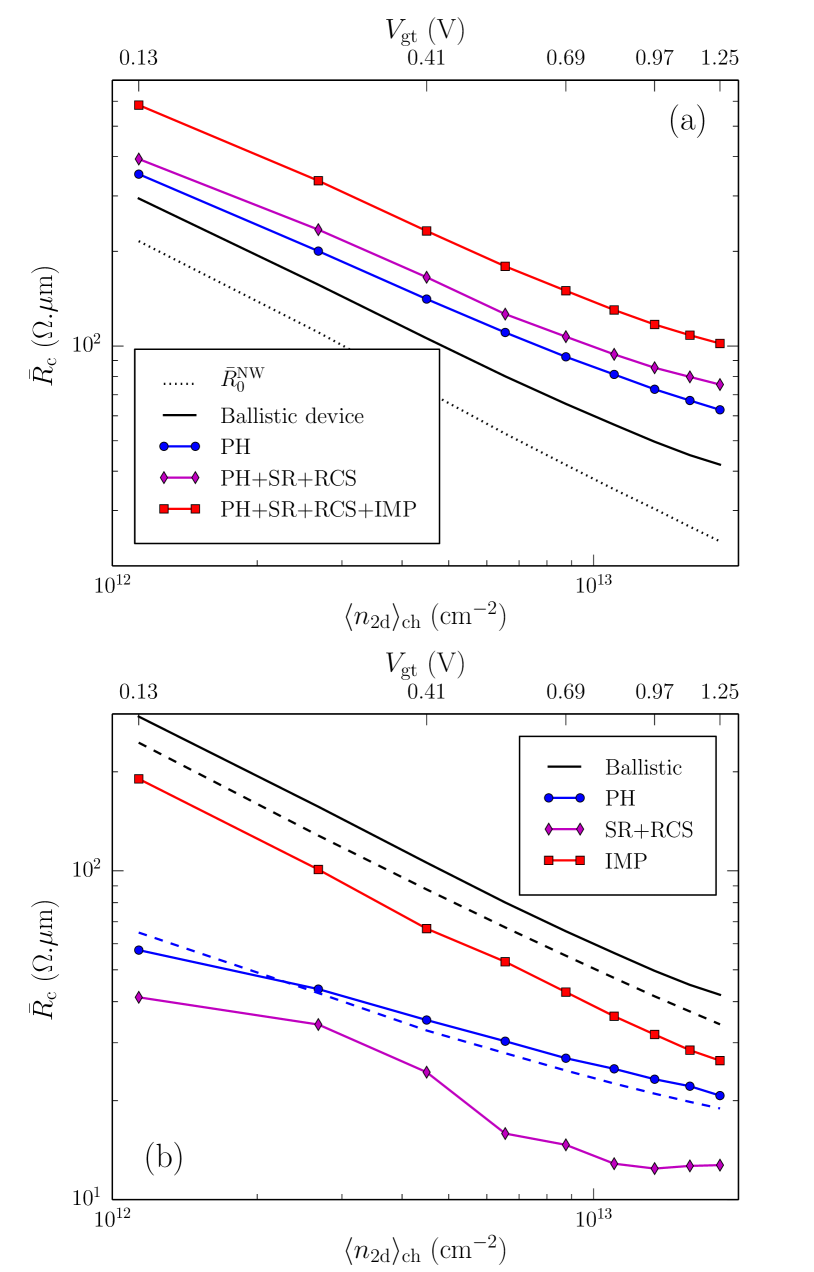
The ballistic resistance is the dominant contribution to , but represents only 40% to 50% of the total contact resistance. The main diffusive component is impurity scattering, followed by phonons, then SR+RCS scattering. As expected, the ratio impurity/phonon scattering decreases with increasing carrier density due to the screening of the ionized impurities by the electron gas under the spacers and gate. The SR+RCS contribution is actually dominated by RCS scattering near both ends of the channel at low densities, and by SR scattering under the spacers at large densities. It is, however, difficult to disentangle these two smaller contributions. Yet SR scattering clearly makes a minor contribution to , while it is a dominant mechanism in the channel. Actually, most of the contacts undergo volume accumulation rather than surface inversion, so that the carriers do not probe much the surface of the spacers. The distribution of carriers under the spacers will be discussed in more detail in the next paragraph.
IV.2 Models and discussion
In order to get a deeper understanding of Fig. 8, we have computed the ballistic resistance of a homogeneous (infinitely long) nm nanowire channel (dotted line in Fig. 8a).Not (a) is significantly lower than the ballistic resistance of the whole device. The cross section and carrier density are, actually, very inhomogeneous in the source/drain and under the spacers. In the simplest “top of the barrier” model,Natori (1994); Rahman et al. (2003) the ballistic resistance of such an inhomogeneous device shall be the ballistic resistance of the homogeneous conductor built from the cross section at the top of the 1D conduction band edge profile . At low bias, the top of the barrier is very close to the point where the carrier density reaches its minimum. We have, therefore, plotted as a dashed black line on Fig. 8b. This simple estimate matches the resistance of the ballistic device much better. The point is under the gate in the subthreshold regime (Fig. 6), but moves under the spacers in the ON regime. The ballistic resistance is then more dependent on the design of the spacers than on the design of the channel, and truly appears in this respect as a “contact” resistance.
We have also attempted to recompute the phonon contribution from a simple local mobility model:
| (8) |
where is the carrier density, the phonon-limited mobility at , and the inversion layer mobility in the channel. The first term is resistance of the whole device, while the second term is the resistance of an ideal channel with homogeneous carrier density . We can further approximate this expression as follows:
| (9) |
where
| (10) |
and is an (arbitrary) reference length. is the difference between the inverse carrier densities integrated in the whole device and in the ideal channel, normalized to . We choose nm, so that Eq. (9) appears as an effective spacer resistance with an effective spacer carrier density . The above approximation on the local mobility is justified by the fact that the main contributions to and are collected under the spacers (where reaches its maximum in the strong inversion regime), and near the entrance/exit of the channel (where the differences between and are the largest). In these regions, can be replaced with , as shows a rather weak dependence on the carrier density. This model, plotted as a dashed blue line in Fig. 8, reproduces the NEGF data very well. It also reproduces the main trends, but is not as accurate for the surface roughness and impurity contributions, whose mobilities show stronger dependences on the carrier density. The carriers indeed move from a “bulk-like” distribution in the source to “surface-inversion-like” distribution in the channel (Fig. 6), so that neither the inversion layer nor the bulk mobilities hold under the spacers. In particular, the SR-limited inversion layer mobility overestimates the surface roughness contribution to . Indeed, can be pretty large near the source/spacer junction, but the carriers are distributed in the bulk of the nanowire, and are, therefore much less scattered by surface roughness than expected from .
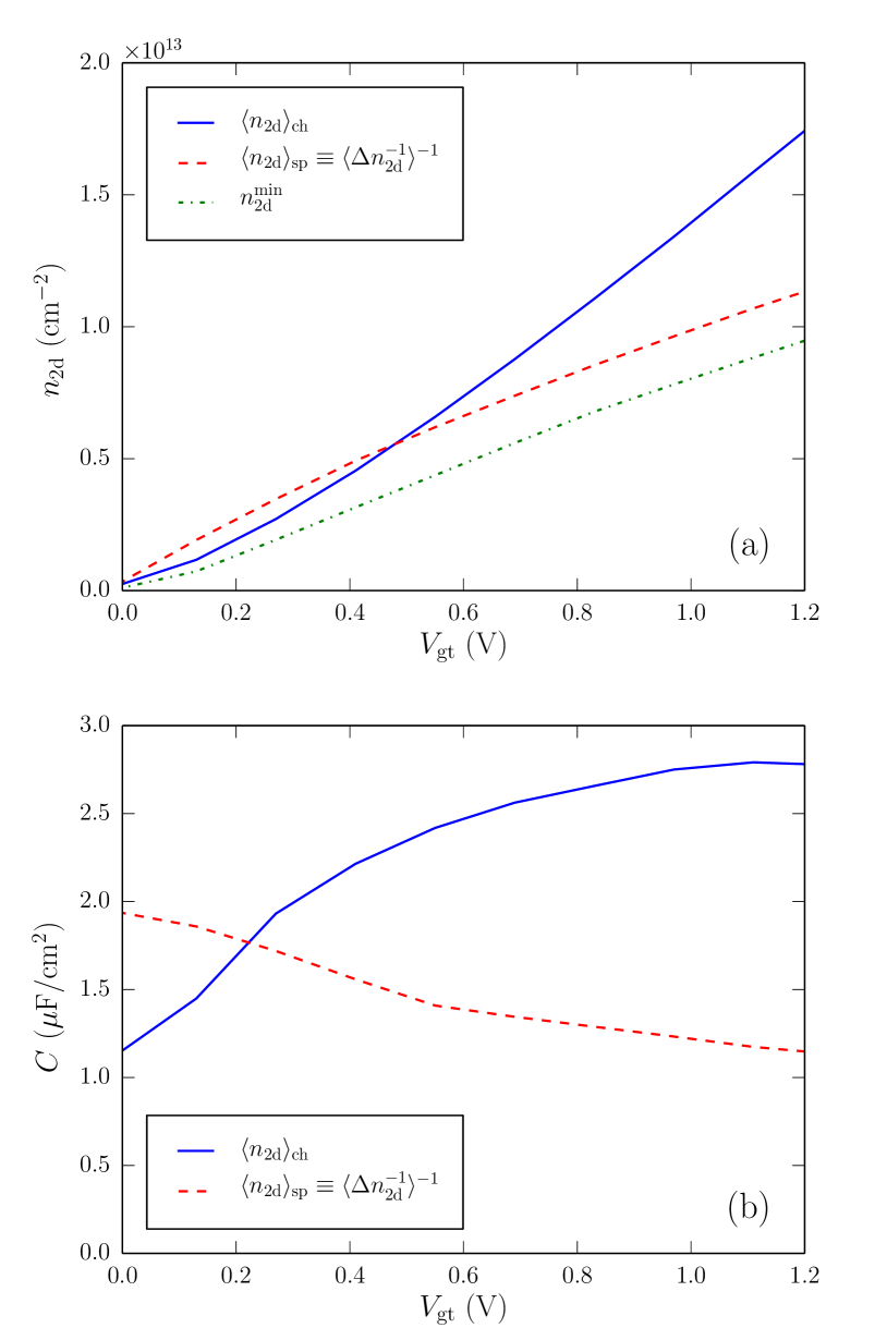
As discussed above, the conductivity of the contacts (as well as the ballistic conductance in the strong inversion regime) are essentially controlled by the density of carriers under the spacers. The latter can be adequately characterized by . By definition [Eq. (10)], the spacers are depleted (as regards transport) with respect to the channel when . and exhibit different dependences on the gate voltage (Figs. 6 and 9). The channel is indeed well controlled by the gate, the gate to channel capacitance reaching a large fraction of the oxide capacitance . On the contrary, the spacers are doped but are poorly controlled by the gate (because they do not overlap). The gate to spacers capacitance is actually much lower than (and weakly dependent on ). The spacers do not, therefore, accumulate much excess charge in the ON regime. In the present device, and cross at gate overdrive V. Above that gate voltage, the carrier density shows a significant dip under the spacers (with density ) that makes a significant contribution to the ballistic and diffusive resistances.
To assess charge control in different devices, we can further approximate and by:
| (11) |
where F/cm2 for all devices considered in this work, and and are threshold voltages for the channel and spacer, respectively.Not (b) There is, therefore, a linear relation between and :
| (12) |
where and is the crossover density. and are characteristic of a design, but do not depend on the channel length (at least in the absence of short-channel effects). As an example, and cm-2 in the nm device of Fig. 9. Data for other devices will be given in the next paragraphs. In the strong inversion regime, is approximately proportional to . It can therefore be written , where is an “effective” spacer mobility (typically in the cm2/V/s range). We would like to stress, though, that embeds the ballistic resistance and shall not, therefore, be interpreted as a diffusive mobility transferable to other spacer lengths.
To conclude, we would like to remind that the present NEGF calculations miss the contribution from the metal/semiconductor contact resistance. The latter is expected to be weakly dependent on , and shall therefore appear as a rigid shift , where is independent of and of (as long as the metal/semiconductor contact remains the same whatever the design of the channel).
V Importance of the design of the near spacer region
As discussed above, the design of the spacers can have a great impact on the contact resistance. We investigate in this section the effect of the cross section of the nanowire (for a given doping profile), then the effect of the doping profile (at constant cross section), and finally the effect of charges trapped in the spacer material.
V.1 Influence of the cross section
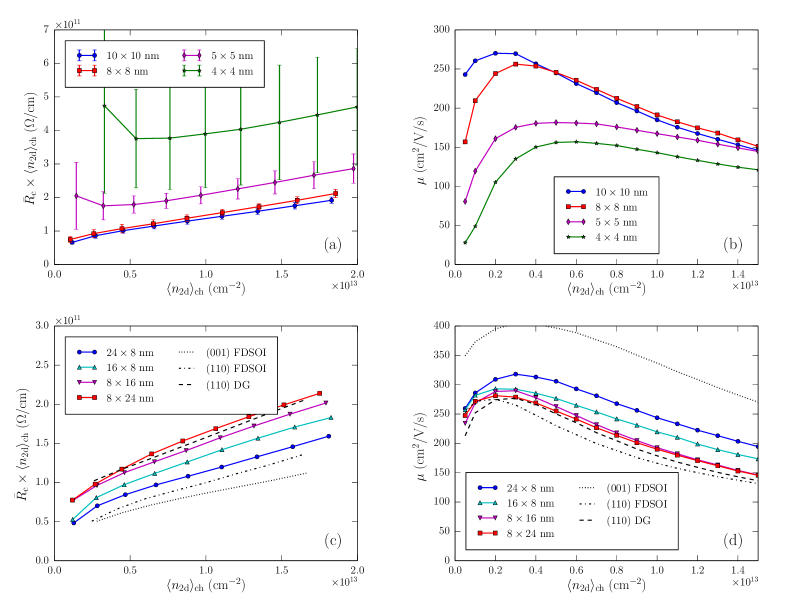
The contact resistance and channel mobility are plotted as a function of the carrier density for trigate and FinFET devices with different cross sections in Fig. 10. They have been extracted from linear regressions on the data on full devices and on homogeneous channels,Niquet et al. (2014) respectively. In order to improve the readability of the figure, we have actually plotted as a function of in Fig. 10a,c. Fig. 10a,b display the results for “square” trigate devices with side ranging from 4 to 10 nm, and Fig. 10c,d the results for horizontal trigate and vertical FinFET devices with either nm or nm. The doping profile is “Reference cm-3” from Fig. 2. The standard deviation on () computed on a set of eight different devices is also reported for square trigate devices as a measure of local variability.
The carrier mobility in the channel of square trigates decreases when the cross section is reduced due to the enhancement of scattering by structural confinement. The picture is, however, very dependent on the carrier density. At high density, inversion mostly takes place at the surface of the nanowire (except in the nm device). Hence the current flows on the top and two side facets, and transport along each facet is mainly limited by SR scattering on that facet. The mobility is, therefore, little dependent on the cross section. The carriers, however, flow closer to the axis of the nanowire when decreasing and , and get eventually scattered by the other facets of the nanowire. This explains the strong dependence of the mobility on the cross section at intermediate carrier densities. At small carrier densities, the transport becomes limited by Remote Coulomb scattering.
In square trigate devices, the normalized contact resistance also tends to increase with decreasing cross section, especially below nm. In the strong inversion regime, is about three times larger in a nm than in a nm device, hence the denormalized contact resistance is almost 7 times larger. The same analysis as in section IV shows that the ballistic and diffusive components of are both enhanced by confinement in the nm device. The main contributors at high inversion are now impurity scattering, then surface roughness scattering, the ballistic resistance, and finally electron-phonon scattering. The increase of diffusive components partly results, as for the channel mobility, from the enhancement of scattering by confinement. Yet the degradation of is mostly due to the decrease of the carrier density under the spacers. The crossover density indeed decreases when reducing cross section (down to cm-2 in the nm trigate), so that the spacers become a strong bottleneck already at weak inversion densities. This results from the decrease of the number of dopants under the spacers and from the increase of the surface to volume ratio. Indeed, on the one hand, the linear density of carriers and conductivity under the spacers are expected to be proportional (in the simplest approximation) to the number of dopants per unit length, . On the other hand, the spacers feed a channel with total width . Therefore, the normalized contact resistance of a square trigate is expected to behave as . As a consequence, the contact resistance can be as large as 75% of the total device resistance in a 30 nm long, nm trigate at gate overdrive V (see Table 1).
The device to device variability also increases a lot when reducing cross section. As the average number of dopants under each spacer decreases from in the nm device to only in the nm device, the fluctuations of the number and position of these dopants have increasing impact on the electrostatics and transport properties of the transistors.Seoane et al. (2009); Martinez et al. (2011); Markov, Cheng, and Asenov (2012)
| (cm-2) | |||||
|---|---|---|---|---|---|
| nm | 1.9 | 0.74 | 0.36 | 0.75 | |
| nm | 3.1 | 0.58 | 0.39 | 0.67 | |
| nm | 8.1 | 0.36 | 0.43 | 0.61 | |
| nm | 12.7 | 0.28 | 0.47 | 0.57 | |
| nm | 16.3 | 0.24 | 0.46 | 0.59 | |
| nm | 24.6 | 0.19 | 0.48 | 0.62 | |
| nm | 16.3 | 0.24 | 0.46 | 0.60 | |
| nm | 24.6 | 0.19 | 0.49 | 0.58 |
The contact resistance and mobility in rectangular trigate and FinFET devices (Figs. 10c, d) also show sizable dependence on the cross section. Actually, vertical FinFET devices with are expected to reach the same contact resistance and mobility as planar , symmetric double-gate (DG) devices,not (a) while horizontal trigate devices with are expected to reach the same contact resistance and mobility as planar FDSOI devices.not (a) is smaller than due to the stronger surface roughness and heavier transport mass along facets [the ground state valley is the valley with transport mass in films and the heavier valleys with transport mass in films]. The mobility is therefore larger in trigate devices with than in FinFET devices with . As an example, the nm trigate shows 30% larger mobility than the nm FinFET at high inversion density ( cm-2). It also shows 30% lower contact resistance, but this performance can hardly be related with the better channel mobilities. As a matter of fact, the contact resistance of planar and FDSOI devices are quite similar while their mobilities are very different (primarily because the spacers do not undergo as strong surface inversion as the channel). Likewise, the denormalized contact resistance of the FinFET and of the nm trigate are very close. As pointed out for square trigates, and confirmed by Fig. 11, is almost inversely proportional to the cross sectional area of the spacers in this range of dimensions (except for the smallest devices). However, the spacers of the vertical FinFET feed a much larger channel ( nm) than those of the horizontal trigate ( nm). This explains why the normalized contact resistance of the vertical FinFETs shows a weak dependence on , and remains very close to the reference double gate device, while the normalized contact resistance of horizontal trigate devices rapidly improves with increasing . In general, devices that maximize effective channel width for a given cross section will show larger normalized contact resistances.
V.2 Influence of the doping profile
| Name | (cm-3) | (nm) | (nm) | (nm) | (cm-2) | ||
|---|---|---|---|---|---|---|---|
| Reference cm-3 | 12.7 | 0.47 | |||||
| Reference cm-3 | 25.4 | 0.61 | |||||
| Strong underlap | 28.4 | 0.67 | |||||
| Small underlap | 32.4 | 0.64 | |||||
| Small overlap | 34.2 | 0.49 |
In this paragraph, we discuss the impact of the doping profile on the contact resistance in a nm trigate device.
We have considered the different doping profiles plotted in Fig. 2. On the source side, the ionized impurity concentration reads:
| (13) |
where is the dopant concentration deep in the source ( cm-3 or cm-3). is approximately equal to when , then decreases by almost one order of magnitude every when , and one order of magnitude every when . In the following, nm is the entrance of the source spacer ( being the entrance of the channel), while can be varied around (see Table 2). The “Reference cm-3” and “Reference cm-3” profiles feature one single decay length nm/decade (), while the other profiles feature two distinct decay lengths. The “small underlap” profile is an optimal distribution resulting from a process simulation. The doping profiles are symmetric under the drain.
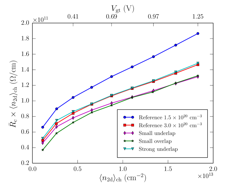
The contact resistances computed in the nm trigate device are plotted as a function of gate overdrive/carrier density in Fig. 12. The devices with cm-3 all show lower resistances than the devices with cm-3. Indeed, larger ’s tend to increase the carrier density in the spacers [larger in Eq. (12)], hence to decrease the contact resistance. As a matter of fact, is greater than cm-2 in all cm-3 devices.
In general, slower decay under the spacer also decreases the contact resistance, as shown by the comparison between the devices with cm-3. The effect is not spectacular though, as in a nm channel the tail of impurities near the gate only contains on average one donor per nanometer at cm-3 – the number of dopants at the entrance/exit of the channel remains therefore very low.
The trends evidenced in Fig. 12 have been confirmed on a nm FinFET device. We would like to point out that the above doping profiles have little impact on the carrier mobilities in the channel, and on the threshold voltage at small . Yet larger and slower decay under the spacers can increase drain-induced barrier lowering at large ; the problem of the contact resistances at high fields is, however, beyond the scope of the present work and will be discussed in an other paper.
V.3 Influence of charges trapped at the Si/Si3N4 interface
Charges trapped in the channel at the Si/SiO2 or SiO2/HfO2 interface are known to be strong scatterers, especially at low carrier densities. In this paragraph, we investigate the effects of charges trapped at the interface between the wire and the spacer material.
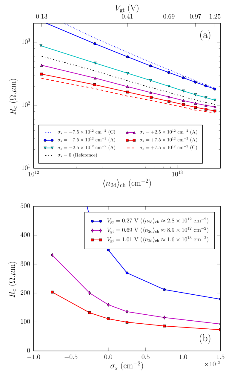
For that purpose, we have computed the contact resistances of a nm trigate device, with different densities of positive or negative charges randomly distributed at the Si/Si3N4 interface. is plotted in Fig. 13, as a function of gate overdrive for a given , and as a function of for different gate overdrives. The threshold voltage and the carrier mobility in the channel are little dependent on the density of traps.
The effects of positive and negative trap charges are opposite. Positive trap charges slightly decrease the contact resistance, whereas negative trap charges strongly increase it. The picture is symmetric for a -type transistor: positive (resp. negative) trap charges increase (resp. decrease) the contact resistance. Also, the effect of the trap charges is almost the same whether they are distributed randomly at the Si/Si3N4 interface [curves labeled “(A)” on Fig. 13], or replaced by a continuous interface charge distribution [curves labeled “(C)” on Fig. 13]. Therefore, the variations of are essentially driven by electrostatics, and not by scattering (at variance with RCS for example).
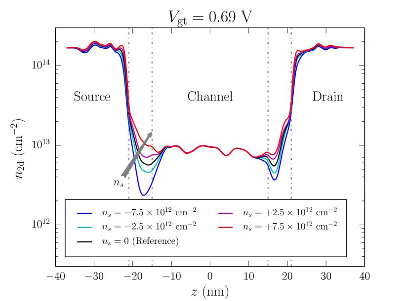
As a matter of fact, interface traps behave as surface dopants, and can therefore enhance accumulation under the spacers ( increases when ), or deplete the wire ( decreases when , see Fig. 14 and Table 3). This either increases () or decreases () the conductivity under the spacers. The effect of these traps shall, therefore, be captured by any method that reproduces the correct electrostatics, including drift-diffusion models.
| (cm-2) | () | (cm-2) | |
|---|---|---|---|
| 0.38 | |||
| 0.45 | |||
| (Reference) | 0.47 | ||
| 0.47 | |||
| 0.48 |
The effects of surface traps increase with increasing surface to volume ratio under the spacers, i.e. with decreasing channel cross section, and with decreasing doping. As an example, is around twice larger in a nm than in a nm trigate at high inversion densities. Interestingly, the contact resistance remains almost the same if a 0.8 nm thick layer of SiO2 is inserted between silicon and Si3N4, and the traps are moved at the SiO2/Si3N4 interface. This results, again, from the electrostatic nature of the mechanism at play here, and can be contrasted with the behavior of RCS in the channel, whose scattering strength decreases exponentially with the thickness of the interfacial layer of SiO2.Casse et al. (2006) The effect of charges trapped in the bulk of the spacers is, as expected, weaker than the effect of charges trapped at the interface with silicon. Namely, in the nm trigate of Fig. 13, where is the density of traps in the bulk of Si3N4, and nm is an effective thickness relating the effects of bulk charges to those of surface charges.
As a consequence of these results, a change of spacer material might improve the contact resistance of one kind of carrier (e.g., electrons) but degrade the contact resistance of the other one (e.g., holes) if the spacer and/or its interface with silicon gets charged differently.
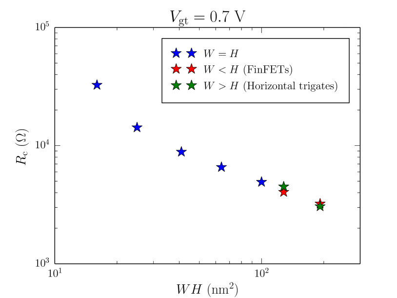
VI Comparison with experimental data
We conclude this work by a comparison with experimental data on trigate devices with cross sections nm and nm fabricated at CEA/LETI.Coquand et al. (2013a) The gate stacks are made of 0.9 nm of SiO2 and 2 nm of HfO2 (effective oxide thickness nm). The spacers are 9 nm long. The target doping in the source and drain is cm-3; the doping profiles are modeled with Eq. (13) using nm, nm, and nm, nm in the source. These values are characteristic of slightly underlapped devices.
The experimental contact resistances and mobilities are extracted with the same transmission line method as in the simulations in the nm range. The data are averaged over 14 devices. The total resistance of the nm device is plotted as a function of gate length in Fig. 15a (with error bars). It shows the expected linear behavior, although there is a small quadratic correction that might be due to the fact that long wires tend to thin in the middle. The mobility in the nm device, measured as the slope of the data, is close to the mobility in nm trigates (Fig. 7), and is in excellent agreement with NEGF calculations. The contact resistances obtained from the linear regressions down to are plotted as a function of in Fig. 15b, for both the nm and the nm devices. They are compared with NEGF simulations for the nm device and for a planar, 12 nm thick FDSOI device.
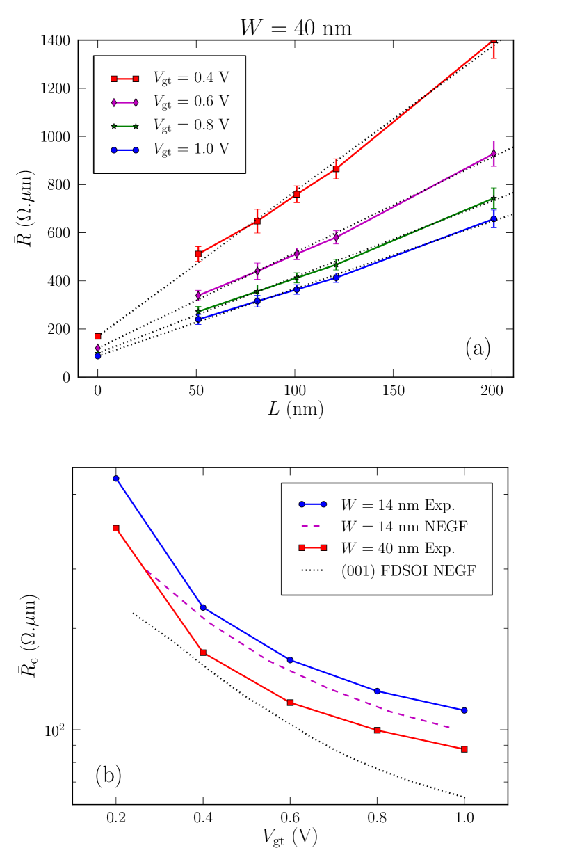
The experimental data show the same dependence as the simulations. The experimental contact resistances for the nm device are, nonetheless, .m larger than the simulations in the V range. We remind, though, that the simulations miss the metal/semiconductor contact resistance, which shall actually be around 20 m.not (b); Ohuchi et al. (2012) The experimental data for the nm device lie, as expected from section V.1, between the simulations for the nm device and for the planar FDSOI device. The larger discrepancies at V might result from the lower accuracy of the extrapolations down to (enhanced device-to-device variability near the threshold and larger slope of the data), and/or from missing Coulomb correlations in the simulations.
The experimental data therefore support the main conclusions of this work about the dependence of the contact resistance on the gate bias and on the cross section. Such a behavior, if not properly accounted for in compact models for the transistors, can strengthen the dependence of the mobility on gate length in short channels.Zilli et al. (2007); Barral et al. (2009); Rideau et al. (2014)
VII Conclusions
We have computed the contact resistance of trigate and FinFET devices using Non-Equilibrium Green’s Functions. At low drain bias, can represent a very large fraction of the total resistance of these devices, so that the design of the source/drain is as or even more important than the design of the channel in sub-20 nm technologies. The spacers between the heavily doped source/drain and the gate are the most resistive parts of the devices and dopant fluctuations under these spacers a major source of variability. The conductance under the spacers is typically limited by the poor electrostatic control over the charge density in these areas. The carrier density can indeed show a dip there, which enhances both ballistic and diffusive components of . As a consequence, the resistance of the spacers has a near dependence, which, if not properly accounted for, can partly explain the apparent dependence of the channel mobility on length in short devices.Zilli et al. (2007); Barral et al. (2009); Rideau et al. (2014) We have investigated the impact of the channel width and height , and the impact of the source/drain doping profiles on the device performances. The contact resistance is more dependent on the cross sectional area of the spacers than on the effective width of the channel. Hence, devices such as FinFETs that maximize the effective width for a given cross sectional area tend to show larger normalized contact resistances . Also, the contact resistance and variability dramatically increase when the cross sectional area of the channel is nm2. Finally, we have shown that defects at the interface between silicon and the spacer material act as surface dopants, which, depending on their charge, improve or degrade the contact resistance.
This work was supported by the French National Research Agency (ANR project NOODLES). The NEGF calculations were run on the TGCC/Curie machine using allocations from PRACE and GENCI.
References
- (1) “The international technology roadmap for semiconductors (itrs),” .
- Kuhn (2012) K. Kuhn, IEEE Transactions on Electron Devices 59, 1813 (2012).
- Jacoboni and Reggiani (1983) C. Jacoboni and L. Reggiani, Reviews of Modern Physics 55, 645 (1983).
- Gamiz and Fischetti (2001) F. Gamiz and M. V. Fischetti, Journal of Applied Physics 89, 5478 (2001).
- Esseni et al. (2003) D. Esseni, A. Abramo, L. Selmi, and E. Sangiorgi, IEEE Transactions on Electron Devices 50, 2445 (2003).
- Uchida and Takagi (2003) K. Uchida and S.-I. Takagi, Applied Physics Letters 82, 2916 (2003).
- Casse et al. (2006) M. Casse, L. Thevenod, B. Guillaumot, L. Tosti, F. Martin, J. Mitard, O. Weber, F. Andrieu, T. Ernst, G. Reimbold, T. Billon, M. Mouis, and F. Boulanger, IEEE Transactions on Electron Devices 53, 759 (2006).
- Jin, Fischetti, and Tang (2007) S. Jin, M. Fischetti, and T.-W. Tang, IEEE Transactions on Electron Devices 54, 2191 (2007).
- Toniutti et al. (2012) P. Toniutti, P. Palestri, D. Esseni, F. Driussi, M. D. Michielis, and L. Selmi, Journal of Applied Physics 112, 034502 (2012).
- Niquet et al. (2014) Y.-M. Niquet, V.-H. Nguyen, F. Triozon, I. Duchemin, O. Nier, and D. Rideau, Journal of Applied Physics 115, 054512 (2014).
- Nguyen et al. (2014) V. Nguyen, Y. Niquet, F. Triozon, I. Duchemin, O. Nier, and D. Rideau, IEEE Transactions on Electron Devices 61, 3096 (2014).
- Niquet et al. (2015) Y. M. Niquet, I. Duchemin, V.-H. Nguyen, F. Triozon, and D. Rideau, Applied Physics Letters 106, 023508 (2015).
- Kotlyar et al. (2004) R. Kotlyar, B. Obradovic, P. Matagne, M. Stettler, and M. D. Giles, Applied Physics Letters 84, 5270 (2004).
- Jin, Fischetti, and wei Tang (2007) S. Jin, M. V. Fischetti, and T. wei Tang, Journal of Applied Physics 102, 083715 (2007).
- Ramayya et al. (2008) E. B. Ramayya, D. Vasileska, S. M. Goodnick, and I. Knezevic, Journal of Applied Physics 104, 063711 (2008).
- Poli et al. (2008) S. Poli, M. Pala, T. Poiroux, S. Deleonibus, and G. Baccarani, IEEE Transactions on Electron Devices 55, 2968 (2008).
- Poli, Pala, and Poiroux (2009) S. Poli, M. Pala, and T. Poiroux, IEEE Transactions on Electron Devices 56, 1191 (2009).
- Persson et al. (2010) M. P. Persson, H. Mera, Y.-M. Niquet, C. Delerue, and M. Diarra, Physical Review B 82, 115318 (2010).
- Neophytou and Kosina (2011) N. Neophytou and H. Kosina, Physical Review B 84, 085313 (2011).
- Lee et al. (2011) J. W. Lee, D. Jang, M. Mouis, G. T. Kim, T. Chiarella, T. Hoffmann, and G. Ghibaudo, Solid-State Electronics 62, 195 (2011).
- Kim et al. (2011) S. Kim, M. Luisier, A. Paul, T. Boykin, and G. Klimeck, IEEE Transactions on Electron Devices 58, 1371 (2011).
- Aldegunde, Martinez, and Asenov (2011) M. Aldegunde, A. Martinez, and A. Asenov, Journal of Applied Physics 110, 094518 (2011).
- Luisier (2011) M. Luisier, Applied Physics Letters 98, 032111 (2011).
- Akarvardar et al. (2012) K. Akarvardar, C. D. Young, M. Baykan, I. Ok, T. Ngai, K.-W. Ang, M. Rodgers, S. Gausepohl, P. Majhi, C. Hobbs, P. Kirsch, and R. Jammy, IEEE Electron Device Letters 33, 351 (2012).
- Nguyen et al. (2013) V.-H. Nguyen, F. Triozon, F. Bonnet, and Y. M. Niquet, IEEE Transactions on Electron Devices 60, 1506 (2013).
- Coquand et al. (2013a) R. Coquand, S. Barraud, M. Cassé, P. Leroux, C. Vizioz, C. Comboroure, P. Perreau, E. Ernst, M.-P. Samson, V. Maffini-Alvaro, C. Tabone, S. Barnola, D. Munteanu, G. Ghibaudo, S. Monfray, F. Boeuf, and T. Poiroux, Solid-State Electronics 88, 32 (2013a).
- Coquand et al. (2013b) R. Coquand, M. Casse, S. Barraud, D. Cooper, V. Maffini-Alvaro, M. Samson, S. Monfray, F. Boeuf, G. Ghibaudo, O. Faynot, and T. Poiroux, IEEE Transactions on Electron Devices 60, 727 (2013b).
- Kim, Park, and Woo (2002a) S.-D. Kim, C.-M. Park, and J. Woo, IEEE Transactions on Electron Devices 49, 457 (2002a).
- Kim, Park, and Woo (2002b) S.-D. Kim, C.-M. Park, and J. Woo, IEEE Transactions on Electron Devices 49, 467 (2002b).
- Dixit et al. (2005) A. Dixit, A. Kottantharayil, N. Collaert, M. Goodwin, M. Jurczak, and K. De Meyer, IEEE Transactions on Electron Devices 52, 1132 (2005).
- Magnone et al. (2008) P. Magnone, V. Subramanian, B. Parvais, A. Mercha, C. Pace, M. Dehan, S. Decoutere, G. Groeseneken, F. Crupi, and S. Pierro, Microelectronic Engineering 85, 1728 (2008).
- Tekleab, Samavedam, and Zeitzoff (2009) D. Tekleab, S. Samavedam, and P. Zeitzoff, IEEE Transactions on Electron Devices 56, 2291 (2009).
- Parada et al. (2011) M. G. Parada, C. Malheiro, P. G. Agopian, and R. C. Giacomini, ECS Transactions 39, 255 (2011).
- Park et al. (2013) S. J. Park, D.-Y. Jeon, L. Montès, S. Barraud, G.-T. Kim, and G. Ghibaudo, Semiconductor Science and Technology 28, 065009 (2013).
- Sohn et al. (2013) C.-W. Sohn, C. Y. Kang, M.-D. Ko, D.-Y. Choi, H. C. Sagong, E.-Y. Jeong, C.-H. Park, S.-H. Lee, Y.-R. Kim, C.-K. Baek, J.-S. Lee, J. Lee, and Y.-H. Jeong, IEEE Transactions on Electron Devices 60, 1302 (2013).
- An et al. (2014) T. An, K. Choe, K.-W. Kwon, and S. Kim, Journal of Semiconductor Technology and Science 14, 425 (2014).
- Pereira and Giacomini (2015) A. Pereira and R. Giacomini, Microelectronics Reliability 55, 470 (2015).
- Yoon et al. (2015) J.-S. Yoon, E.-Y. Jeong, S.-H. Lee, Y.-R. Kim, J.-H. Hong, J.-S. Lee, and Y.-H. Jeong, Japanese Journal of Applied Physics 54, 04DC06 (2015).
- Berrada et al. (2015) S. Berrada, M. Bescond, N. Cavassilas, L. Raymond, and M. Lannoo, Applied Physics Letters 107, 153508 (2015).
- Colinge (2004) J.-P. Colinge, Solid-State Electronics 48, 897 (2004).
- Anantram, Lundstrom, and Nikonov (2008) M. P. Anantram, M. S. Lundstrom, and D. E. Nikonov, Proceedings of the IEEE 96, 1511 (2008).
- (42) W. Shockley, “Research and investigation of inverse epitaxial UHF power transistors”, Report No. A1-TOR-64-207, Air Force Atomic Laboratory, Wright-Patterson Air Force Base, Ohio, September 1964.
- (43) The system is therefore modeled as a periodic array of nanowires connected to thick source and drain films. The convergence with respect to , and has been carefully checked.
- Goodnick et al. (1985) S. M. Goodnick, D. K. Ferry, C. W. Wilmsen, Z. Liliental, D. Fathy, and O. L. Krivanek, Physical Review B 32, 8171 (1985).
- (45) The probability to find a dopant at at given point of the source is proportional to the background dopant concentration shown in Fig. 2. A distribution of point charges is picked randomly, and mixed with near the edge of the simulation box: , where , with nm and nm.
- Stefanucci and van Leeuwen (2013) G. Stefanucci and R. van Leeuwen, Nonequilibrium Many-Body Theory of Quantum Systems: A Modern Introduction (Cambridge University Press, 2013).
- Bastard (1988) G. Bastard, Wave mechanics applied to semiconductor heterostructures (Les Éditions de Physique, 1988).
- Sze and Kwok (2006) M. S. Sze and K. N. Kwok, Physics of Semiconductor Devices (John Wiley and Sons, New-York, 2006).
- Fischetti et al. (2009) M. Fischetti, S. Jin, T.-W. Tang, P. Asbeck, Y. Taur, S. Laux, M. Rodwell, and N. Sano, Journal of Computational Electronics 8, 60 (2009).
- Li, Bescond, and Lannoo (2009) C. Li, M. Bescond, and M. Lannoo, Phys. Rev. B 80, 195318 (2009).
- Lavieville et al. (2015) R. Lavieville, F. Triozon, S. Barraud, A. Corna, X. Jehl, M. Sanquer, J. Li, A. Abisset, I. Duchemin, and Y.-M. Niquet, Nano Letters 15, 2958 (2015).
- Seoane et al. (2009) N. Seoane, A. Martinez, A. Brown, J. Barker, and A. Asenov, IEEE Transactions on Electron Devices 56, 1388 (2009).
- Martinez et al. (2011) A. Martinez, M. Aldegunde, N. Seoane, A. Brown, J. Barker, and A. Asenov, IEEE Transactions on Electron Devices 58, 2209 (2011).
- Datta, Assad, and Lundstrom (1998) S. Datta, F. Assad, and M. Lundstrom, Superlattices and Microstructures 23, 771 (1998).
- Shur (2002) M. Shur, IEEE Electron Device Letters 23, 511 (2002).
- Ghibaudo (1988) G. Ghibaudo, Electronics Letters 24, 543 (1988).
- Rideau et al. (2014) D. Rideau, F. Monsieur, O. Nier, Y. Niquet, J. Lacord, V. Quenette, G. Mugny, G. Hiblot, G. Gouget, M. Quoirin, L. Silvestri, F. Nallet, C. Tavernier, and H. Jaouen, in 2014 International Conference on Simulation of Semiconductor Processes and Devices (SISPAD) (2014) pp. 101–104.
- Rhew, Ren, and Lundstrom (2002) J.-H. Rhew, Z. Ren, and M. S. Lundstrom, Solid-State Electronics 46, 1899 (2002).
- Büttiker et al. (1985) M. Büttiker, Y. Imry, R. Landauer, and S. Pinhas, Physical Review B 31, 6207 (1985).
- Datta (1995) S. Datta, Electronic Transport in Mesoscopic Systems (Cambridge University Press, Cambridge, 1995).
- Jacoboni et al. (1977) C. Jacoboni, C. Canali, G. Ottaviani, and A. A. Quaranta, Solid State Electronics 20, 77 (1977).
- Not (a) (a), can either be obtained from a ballistic NEGF calculation in a homogeneous nanowire or from the band structure of that nanowire (see, e.g., Refs. Natori, 1994 and Rahman et al., 2003).
- Natori (1994) K. Natori, Journal of Applied Physics 76, 4879 (1994).
- Rahman et al. (2003) A. Rahman, J. Guo, S. Datta, and M. Lundstrom, IEEE Transactions on Electron Devices 50, 1853 (2003).
- Not (b) (b), can be slightly different from defined in paragraph II.3, as the former is based on a density criterion, and the latter on a current criterion.
- not (a) (a), the planar FDSOI device used for comparison in Fig. 10 is a 8 nm thick Si film on a 25 nm thick BOX with the same gate stack and surface roughness parameters as the trigate devices (namely nm and nm on the bottom interface with the BOX, nm and nm on the top interface with the gate stack). The planar FDSOI device is the same, but with nm and nm on both top and bottom interfaces. The planar double-gate device is, likewise, a symmetric stucture with a 8 nm thick film, and nm, nm on both interfaces.
- Markov, Cheng, and Asenov (2012) S. Markov, B. Cheng, and A. Asenov, IEEE Electron Device Letters 33, 315 (2012).
- not (b) (b), the source and drain can be modeled as nm pads with contact resistivities .cm2. For a typical effective width nm, these pads therefore make a contribution to the contact resistance m.
- Ohuchi et al. (2012) K. Ohuchi, C. Lavoie, B. Yang, M. Kondo, K. Matsuzawa, and P. M. Solomon, Japanese Journal of Applied Physics 51, 101302 (2012).
- Zilli et al. (2007) M. Zilli, D. Esseni, P. Palestri, and L. Selmi, IEEE Electron Device Letters 28, 1036 (2007).
- Barral et al. (2009) V. Barral, T. Poiroux, D. Munteanu, J. Autran, and S. Deleonibus, IEEE Transactions on Electron Devices 56, 420 (2009).